Note: Descriptions are shown in the official language in which they were submitted.
CA 02324600 2003-02-07
INTEGRATED MICRO-OPTICAL SYSTEMS
BACI~GIZ.OUND OF THE INVENTION
Field of the Invention
The present invention is directed to integrating optics on the wafer level
with an active element, particularly for use with magneto-optic heads.
Description of Related Art
Magneto-optical heads are used to read current high-density magneto-optic
media. In particular, a magnetic coil is used to apply a magnetic field to the
media
and light is then also delivered to the media to write to the media. The light
is also
used to read from the media in accordance with the altered characteristics of
the
media from the application of the magnetic field and light.
An example of such a configuration is shown in Figure 1. In Figure l, an
optical fiber 8 delivers light to the head. The head includes a slider block
10
which has an objective lens 12 mounted on a side thereof. A mirror 9, also
mounted on the side of the slider block 10, directs Iight from the optical
fiber 8
onto the objective lens 12. A magnetic coil 14, aligned with the lens 12, is
also
CA 02324600 2000-09-19
WO 99149455 PCT/US99/06661
-2-
mounted on the side of the slider block 10. The head sits on top of an air
bearing
sandwich 16 which is between the head and the media 18. The slider block 10
allows the head to slide across the media 18 and read from or write to the
media
18.
The height of the slider block 10 is limited, typically to between 500-1500
microns, and is desirably as small as possible. Therefore, the number of
lenses
which could be mounted on the slider block is also limited. Additionally,
alignment of more than one lens on the slider block is difficult. Further, due
to the
small spot required, the optics or overall optical system of the head need to
have
a high numerical aperture, preferably greater than .6. This is difficult to
achieve
in a single objective lens due to the large sag associated therewith. The
overall
head is thus difficult to assemble and not readily suited to mass production.
SUMMARY OF THE INVENTION
Therefore, it is an object of the present invention to provide a slider block
having an active element, i.e., an element having a characteristic which
changes
in response to an applied field, integrated thereon which substantially
overcomes
one or more ofthe problems due to the limitations and disadvantages of the
related
art. Such elements include a magnetic coil, a light source, a detector, etc.
It is a further object of the present invention to integrate multiple optical
elements and a slider block having the active element integrated thereon as
well.
It is a further object of the present invention to manufacture the objects on
a wafer
CA 02324600 2000-09-19
WO 99/49455 PCT/US99/06661
-3
level, bond a plurality of wafers together and provide the active element on a
bottom surface of a bottom wafer.
At least one of the above and other advantages may be realized by
providing an integrated micro-optical system including a die formed from more
S than one wafer bonded together, each wafer having a top surface and a bottom
surface, bonded wafers being diced to yield multiple dies and an active
element
having a characteristic which changes in response to an applied field,
integrated
on a bottom surface of the die, optical elements being formed on more than one
surface of the die.
The active element may be a thin film conductor whose magnetic properties
changes when a current is applied thereto. The active element may be
integrated
as an array of active elements on the bottom wafer before the bonded wafers
are
diced. The die may be formed from two wafers and optical elements are formed
on a top surface and a bottom surface of a top wafer and a top surface of the
bottom wafer. The die may include a high numerical aperture optical system.
The bottom wafer of the more than one wafer may have a higher index of
refraction than other wafers. There may be no optical elements on a bottom
wafer
of the die. The bottom surface of the die may further include features for
facilitating sliding of the integrated micro-optical system etched thereon.
The
bottom wafer of the die may have a refractive element formed in a material of
high
numerical aperture. Metal portions serving as apertures may be integrated on
at
least on one the surfaces of the die.
CA 02324600 2000-09-19
WO 99/49455 PCT/US99/06661
-4-
A layer of material deposited on the bottom surface of the bottom wafer
before the active element is integrated thereon. An optical element may be
formed
on the bottom surface of the bottom wafer, wherein the layer has a refractive
index
that is different from the refractive index of the bottom wafer. The layer may
be
deposited in accordance with a difference between a desired thickness and a
measured thickness.
A monitoring optical system may be formed on each surface of the wafer
containing an optical element. The spacing between wafers may be varied in
accordance with a difference between a measured thickness of a wafer and a
desired thickness of a wafer.
A top surface of the die may be etched and coated with a reflective coating
to direct light onto the optical elements. A further substrate may be mounted
on
top of the top of the die having a MEMS mirror therein. An insertion point may
be provided on the die for receiving an optical fiber therein. The insertion
point
may be on a side of the die and the system further includes a reflector for
redirecting light output by the fiber.
A refractive element in the die may be a spherical lens and the die further
includes a compensating element which compensates for aberrations exhibited by
the spherical lens. The compensating element may be on a surface immediately
adjacent the spherical lens. The compensating element may be a diffractive
element. The refractive element may be an aspheric lens. The die may include
at
CA 02324600 2000-09-19
WO 99/49455 PCT/US99/06661
-5
least one additional refractive element, all refractive elements of the die
being
formed in material having a high numerical aperture.
At least one of the above and other advantages may be realized by
providing an integrated micro-optical apparatus including a die formed from
more
than one wafer bonded together, each wafer having a top surface and a bottom
surface, bonded wafers being diced to yield multiple die, at least two optical
elements being formed on respective surfaces of each die, at least one of the
at
least two optical elements being a refractive element, a resulting optical
system of
each die having a high numerical aperture.
The refractive element may be a spherical lens and the die further includes
a compensating element which compensates for aberrations exhibited by the
spherical lens. The compensating element may be on a surface immediately
adjacent the spherical lens. The compensating element may be a diffractive
element. The refractive element may be an aspheric lens.
The die may include at least one additional refractive element, all refractive
elements of the die being formed in material having a high numerical aperture.
The refractive element may be on a bottom wafer and of a material having a
higher
refractive index than that of the bottom wafer.
Further scope of applicability of the present invention will become apparent
from the detailed description given hereinafter. However, it should be
understood that
the detailed description and specific examples, while indicating preferred
embodiments of the invention, are given by way of illustration only, since
various
CA 02324600 2000-09-19
WO 99/49455 PCT1US99/06661
-6-
changes and modifications within the spirit and scope of the invention will
become
apparent to those skilled in the art from this detailed description.
BRIEF DESCRIPTION OF THE DRAWINGS
The present invention will become more fully understood from the detailed
description given herein below and the accompanying drawings which are given
by
way of illustration only, and thus are not limitative of the present
invention, and
wherein:
Figure 1 illustrates a configuration of a high-density flying head magneto-
optical read/write device;
Figure 2A illustrates one configuration for the optics to be used in forming a
slider block;
Figure 2B illustrates the spread function of the optical system shown in
Figure
2A;
Figure 3A illustrates a second embodiment of the optics for use in sliding
block of the present invention;
Figure 3B illustrates the spread function of the optical system shown in
Figure
3A;
Figure 4A illustrates a third embodiment of an optical system to be used in
the
slider block of the present invention;
Figure 4B illustrates the spread function of the optical system shown in
Figure
4A;
CA 02324600 2000-09-19
WO 99/49455 PCT/US99/06661
_'j_
Figure 5 is a side view of an embodiment of a slider block in accordance with
the present invention;
Figure 6 is a side view of another embodiment of a slider block in accordance
with the present invention;
Figure 7 is a side view of another embodiment of a slider block in accordance
with the present invention;
Figure 8A is a side view of another embodiment of a slider block in
accordance with the present invention; and
Figure 8B is a bottom view of the embodiment in Figure 8A.
DETAILED DESCRIPTION OF THE PREFERRED EMBODIMENTS
All ofthe optical systems shown in Figures 2A-4B provide satisfactory results,
i.e., a high numerical aperture with good optical performance. The key element
in
these optical systems is the distribution of the optical power over multiple
available
surfaces. Preferably this distribution is even over the multiple surfaces.
Sufficient
distribution for the high numerical aperture required is realized over more
than one
surface. Due to the high numerical aperture required, this distribution of
optical power
reduces the aberrations from the refractive surfaces and increases the
diffractive
efficiency of the diffractive surfaces by reducing the deflection angle
required from
each surface.
Further, a single refractive surface having a high numerical aperture would be
difficult to incorporate on a wafer, since the increased curvature required
for affecting
CA 02324600 2000-09-19
WO 99/49455 PC'T/US99/06661
_g_
such a refractive surface would result in very thin portions of a typical
wafer, leading
to concerns about fragility, or would require a thick wafer, which is not
desirable in
many applications where size is a major constraint. Further, the precise shape
control
required in the manufacture of a single refractive surface having high NA
would
present a significant challenge. Finally, the surfaces having the optical
power
distributed are easier to manufacture, have better reproducibility, and
maintain a better
quality wavefront.
In accordance with the present invention, more than one surface may be
integrated with an active element such as a magnetic coil by bonding wafers
together.
Each wafer surface can have optics integrated thereon photolithographically,
either
directly or through molding or embossing. Each wafer contains an array of the
same
optical elements. When more than two surfaces are desired, wafers are bonded
together. When the wafers are diced into individually apparatuses, the
resulting
product is called a die. The side views of Figs. 2A, 3A, and 4A illustrate
such dies
which consist of two or three chips bonded together by a bonding material 25.
In the example shown in Figure 2A, a diffractive surface 20 is followed by a
refractive surface 22, which is followed by a diffractive surface 24, and then
finally
a refractive surface 26. In the example shown in Figure 3A, a refractive
surface 30
is followed by a diffractive surface 32, which is followed by a refractive
surface 34
which is finally followed a dif&active surface 36. In the optical system shown
in
Figure 4A, a refractive surface 40 is followed by a diffractive surface 42
which is
followed by a refractive surface 44 which is followed by a diffractive surface
46,
CA 02324600 2000-09-19
WO 99/49455 PCT/US99/06661
-9
which is followed by a refractive surface 48 and finally a diffractive surface
50. The
corresponding performance of each of these designs is shown in the
corresponding
intensity spread function of Figs. 2B, 3B, and 4B.
When using spherical refractive elements as shown in Figures 2A, 3A and 4A,
it is convenient to follow these spherical refractive elements with a closely
spaced
diffractive element to compensate for the attendant spherical aberration. An
aspherical refractive does not exhibit such aberrations, so the alternating
arrangement
of refractives and diffractives will not necessarily be the preferred one.
While the optical elements may be formed using any technique, to achieve the
required high numerical aperture, it is preferable that the refractive lenses
remain in
photoresist, rather than being transferred to the substrate. It is also
preferable that the
bottom substrate, i.e., the substrate closest to the media, has a high index
of refraction
relative of fused silica, for which n=1.36. Preferably, this index is at least
.3 greater
than that of the substrate. One example candidate material, SF56A, has a
refractive
index of 1.785. If the bottom substrate is in very close proximity to the
media, e.g.,
less than 0.5 microns, the use of a high index substrate allows a smaller spot
size to
be realized. The numerical aperture N.A. is defined by the following:
N.A. = n sin A
where n is the refractive index of the image space and 8 is the half angle of
the
maximum cone of light accepted by the lens. Thus, if the bottom substrate is
in very
close proximity to the media, the higher the index of refraction of the bottom
CA 02324600 2000-09-19
WO 99/49455 PCT/US99/06661
-10-
substrate, the smaller the acceptance half angle for the same performance.
This
reduction in angle increases the efficiency of the system.
As shown in Figure 5, the slider block 61 in accordance with the present
invention includes a die composed of a plurality of chips, each surface of
which is
available for imparting optical structures thereon. The die is formed from
wafers
having an array of respective optical elements formed thereon on either one or
both
surfaces thereof. The individual optical elements may be either diffractive,
refractive
or a hybrid thereof. Bonding material 25 is placed at strategic locations on
either
substrate in order to facilitate the attachment thereof. By surrounding the
optical
elements which are to form the final integrated die, the bonding material or
adhesive
25 forms a seal between the wafers at these critical junctions. During dicing,
the seal
prevents dicing slurry from entering between the elements, which would result
in
contamination thereof. Since the elements remain bonded together, it is nearly
impossible to remove any dicing slurry trapped there between. The dicing
slurry
presents even more problems when diffractive elements are being bonded, since
the
structures of diffractive elements tend to trap the slurry.
Advantageously, the wafers being bonded include fiducial marks somewhere
thereon, most likely at an outer edge thereof, to ensure alignment of the
wafers so that
all the individual elements thereon are aligned simultaneously. Alternatively,
the
fiducial marks may be used to facilitate the alignment and creation of
mechanical
alignment features on the wafers. One or both of the fiducial marks and the
alignment
features may be used to align the wafers. The fiducial marks and/or alignment
features
CA 02324600 2000-09-19
WO 99!49455 PCT/US99/06661
-11
are also usefial in registering and placing the active elements and any
attendant
structure, e.g., a metallic coil and contact pads therefor, on a bottom
surface. These
active elements could be integrated either before or after dicing the wafers.
On a bottom surface 67 of the slider block 61 in accordance with the present
invention, a magnetic head 63 including thin film conductors and/or a magnetic
coil
is integrated using thin film techniques, as disclosed, for example, in U.S.
Patent No.
5,314,596 to Shukovsky et al. Entitled "Process for Fabricating Magnetic Film
Recording Head for use with a Magnetic Recording Media." The required contact
pads for the magnetic coil are also preferably provided on this bottom
surface.
Since the magnetic coil 63 is integrated on the bottom surface 67, and the
light
beam is to pass through the center of the magnetic coil, it is typically not
practical to
also provide optical structures on this bottom surface. This leaves the
remaining five
surfaces 50-58 available for modification in designing an optical system.
Further,
additional wafers also may be provided thereby providing a total of seven
surfaces.
With the examples shown in Figs. 2A and 3A the surface SO would correspond to
surface 20 or 40, respectively, the surface 52 would correspond to surface 22
or 32,
respectively, the surface 54 would correspond to surface 24 or 34,
respectively, and
the surface 56 would correspond to surface 26 or 36, respectively.
Each of these wafer levels can be made very thin, for example, on the order of
125 microns, so up to four wafers could be used even under the most
constrained
conditions. If size and heat limitations permit, a light source could be
integrated on the
top of the slider block, rather than using the fiber for delivery of light
thereto. In
CA 02324600 2003-02-07
-12-
addition to being thin, the use of the wafer scale assembly allows accurate
alignment
of numerous objects, thereby increasing the number of surfaces containing
optical
power, which can be used. This wafer scale assembly also allows use of passive
alignment techniques. The other dimensions ofthe slider block 61 are
determined by
J the size of the pads for the magnetic coil, which is typically 1500 microns,
on the
surface 67, which is going to be much larger than any of the optics on the
remaining
surfaces, and any size needed for stability of the slider block 61. The bottom
surface
67 may also include etch features thereon which facilitate the sliding of the
slider
block 61.
Many configurations of optical surfaces may be incorporated into the slider
block 61. The bonding, processing, and passive alignments of wafers is
disclosed
in co-pending, commonly assigned U.S. Patent No. 5,771,218 entitled
"Integrated
Optical Head for Disk Drives and Method of Forming Same" and U.S. Patent No.
6,096,155 entitled "Wafer Level Integration of Multiple Optical Heads".
Additionally, an optical element can be provided on the bottom surface 67 of
the bottom wafer as shown in Figure 6. When providing an optical element on
this
bottom surface 67, a transparent layer 65, having a different refractive index
than that
of the wafer itself is provided between the bottom surface 67 and the coil 63.
The
difference in refractive index between the layer 65 and the wafer should be at
least
approximately 0.3 in order to insure that the optical effect of the optical
element
provided on the bottom surface 67 is discernable. Also as shown in Figure 6, a
single
CA 02324600 2000-09-19
WO 99/49455 PC'T/US99/06661
-13
wafer may be used if su~cient performance can be obtained from one or two
optical
elements.
Further as shown in Figure 6, metal portions 69 may be provided to serve as
an aperture for the system. These apertures may be integrated on any of the
wafer
surfaces. The aperture may also serve as the aperture stop, typically
somewhere in the
optical system prior to the bottom surface thereof. When such metal portions
69
serving as an aperture are provided on the bottom surface 67, it is
advantageous to
insure the metal portions 69 do not interfere with the operation of the metal
coil 63.
A problem that arises when using a system with a high numerical aperture for
a very precise application is that the depth of focus of the system is very
small.
Therefore, the distance from the optical system to the media must be very
precisely
controlled to insure that the beam is focused at the appropriate position of
the media.
For the high numerical apertures noted above, the depth of focus is
approximately 1
micron or less. The thicknesses of the wafers can be controlled to within
approximately 1-5 microns, depending on the thickness and diameter of the
wafer.
The thinner and smaller the wafer, the better the control. When multiple
wafers are
used, the system is less sensitive to a variation from a design thickness for
a particular
wafer, since the power is distributed through all the elements.
When using multiple wafers, the actual thickness of each wafer can be
measured and the spacing between the wafers can be adjusted to account for any
deviation. The position of the fiber or source location can be adjusted to
correct for
thickness variations within the wafer assembly. Alternatively, the design of a
CA 02324600 2000-09-19
WO 99/49455 PCT/US99/06661
-14
diffractive element may be altered in accordance with a measured thickness of
the
slider block in order to compensate for a variation from the desired
thickness.
Alternatively, the entire system may be designed to focus the light at a
position deeper
than the desired position assuming the thicknesses are precisely realized.
Then, the
layer 65 may be deposited to provide the remaining required thickness to
deliver the
spot at the desired position. The deposition of the layer 65 may be more
precisely
controlled than the formation of the wafers, and may be varied to account for
any
thickness variation within the system itself, i.e., the layer 65 does not have
to be of
uniform thickness. If no optical element is provided on the bottom surface 67,
then the
refractive index of the layer 65 does not need to be different from that of
the wafer.
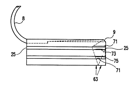
Figure 7 is a side view of another embodiment of the slider block. As shown
in Figure 7, the fiber 8 is inserted into the top wafer and the mirror 9 is
integrated into
the top wafer, preferably at a 45-degree angle. Light reflected by the mirror
9 is
directed to a diffractive element 71, followed by a refractive element 73,
followed by
a diffractive element 75, followed by a refractive element 77, and delivered
through
the coil 63. For such a configuration, the top surface 50 is no longer
available for
providing an optical element.
Additionally, for fine scanning control of the light, the mirror 9 may be
replaced with a micro-electro-mechanical system (MEMS) mirror mounted on a
substrate on top of the top chip. A tilt angle of the MEMS is controlled by
application
of a voltage on a surface on which the reflector is mounted, and is varied in
CA 02324600 2000-09-19
WO 99!49455 PCT/US99/06661
-15
accordance with the desired scanning. The default position will preferably.by
45
degrees so the configuration will be the same as providing the minor 9.
An additional feature for monitoring the spot of light output from the slider
block is shown in Figures 8A and 8B. As shown in Figure 8A, in addition to the
optical system, consisting of, for example, diffractive elements 87, 89, used
for
delivering light through the magnetic coil 63, monitoring optical elements 81,
83 are
provided. The monitoring optical elements 81, 83 are of the same design as the
elements of the optical system 87, 89, respectively. In other words, the
monitoring
optical elements are designed to focus at a same distance as that of the
optical system.
Advantageously, the monitoring optical elements 81, 83 are larger than the
optical
system elements for ease of construction and alignment of the test beam. In
the
configuration shown in Figures SA and 8B, the monitoring optical elements 81,
83 are
approximately twice the size of the element 87, 89. The monitoring system also
includes an aperture 85, preferably foamed by metal. It is noted that Figure
8B does
not show the magnetic coil 63.
During testing, light is directed to the monitoring optical system to insure
that
light is being delivered to the aperture at the desired location. The
magnitude of light
passing through the aperture will indicate if the optical system is
sufficiently accurate,
i.e., that the light is sufficiently focused at the aperture to allow a
predetermined
amount of light through. If the light is not sufficiently focused, the
aperture will block
too much of the light.
Thus, by using the monitoring system shown in Figures 8A and 8B, the optical
system of the slider block may be tested prior to its insertion into the
remaining
CA 02324600 2000-09-19
WO 99/49455 PCT/US99/06661
-16
device, even after being integrated with the active element 63. The dimension
requirement imposed by the contact pads for the magnetic coil 63 and the coil
itself
result in sufficient room available on the wafers for the inclusion of such a
monitoring
system, so the size of the slider block is unaffected by the incorporation of
the
monitoring system.
The invention being thus described, it will be obvious that the same may be
varied in many ways. Such variations are not to be regarded as a departure
from the
spirit and scope of the invention, and all such modifications as would be
obvious to
one skilled in the art are intended to be included within the scope of the
following
claims.