Note: Descriptions are shown in the official language in which they were submitted.
CA 02324808 2000-10-31
SEMICONDUCTOR LASER MODULE
FIELD OF THE INVENTION
This invention relates to a semiconductor laser module, and
especially to a semiconductor laser module of 980 nm band.
BACKGROUND OF THE INVENTION
A radiation pattern of a semiconductor laser diode of 980 nm
band is elliptic, a half-width angle thereof in the vertical plane
is 20' to 40' , and that in the horizontal plane is 5~ to 15~ .
When the semiconductor laser diode of the 980 nm band is optically
coupled with an optical fiber, a mode field diameter of which is
almost circular, a coupling loss therebetween becomes excessively
large.
In an attempt to overcome the aforementioned difficulty, an
experiment that a laser beam emitted from the semiconductor laser
diode of the 980 nmband is focused bya cylindrical lens is conducted.
In this experiment, the laser beam is focused only in the vertical
plane with intent to make the shape of the radiation pattern of
the laser beam be nearly circular. However, since the laser beam
is not focused in the horizontal plane, a coupling efficiency between
the semiconductor laser diode and the optical fiber cannot be improved .
Although the use of a beam-shaping lens or an optical fiber with
an elliptic cross-section has been proposed as another method for
solving the aforementioned difficulty, there is a problem that a
structure becomes complicated or the optical fiber is hard to be
processed.
CA 02324808 2000-10-31
-2-
As a devise for solving the aforementioned problems and improving
the coupling efficiency between the semiconductor laser diode and
the optical fiber, there is a method that the optical fiber is so
processed that an input end portion thereof tapers off to a point.
S According to this method, the end portion of the optical fiber
is easilyprocessed by polishing. Moreover, since the optical fiber
closely approaches the semiconductor laser, it is out of the question
that the laser beam is not focused in the vertical plane.
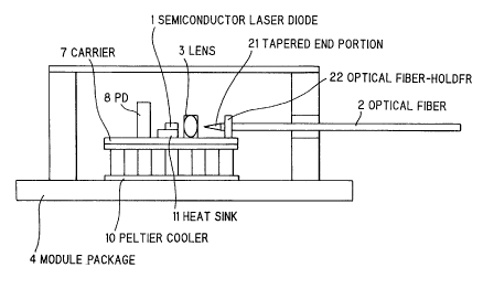
As shown in FIG.1, in the aforementioned semiconductor module,
the semiconductor laser diode 1 is mounted on a heat sink 11 and
fixed to a carrier 7 by soldering.
The carrier 7 is fixed to the cooling substrate of a Peltier
cooler 10 which controls temperature of the semiconductor laser
diode 1 in order to stabilized a power level and a lasing wavelength
of an optical signal. The Peltier cooler 10 is fixed to an internal
bottom surface of a module package 4.
A photodiode ( a PD, hereinafter ) 8 for monitoring outputted
light power of the semiconductor laser diode 1 is mounted on the
carrier 7. The optical fiber 2 is fixed to the carrier 7 via an
optical fiber-holder 22 so that a tapered end portion 21 of the
optical fiber 2 approaches the semiconductor laser diode 1 closely.
A clearance between the module package 4 and the optical fiber
2 is filled with solder with a low melting point in order to airtightly
seal the semiconductor laser diode 1.
As shown in FIG . 2 , an optical conf iguration of the conventional
semiconductor module is composed of the semiconductor laser diode
1 and the tapered end portion 21 of the optical fiber 2 only. In
CA 02324808 2000-10-31
-3-
FIG.2, the light emitted from the semiconductor laser diode 1 is
concentrated on the optical fiber 2, and taken out through the optical
fiber 2 and transmitted towards the outside. In this case, an interval
between the semiconductor laser diode 1 and the optical fiber 2
is L2 under the optimum condition of the optical coupling.
However, in the aforementioned structure, since the interval
between the optical fiber 2 and the semiconductor laser diode 1
under the optimum condition of the optical coupling is several tens
,(.lm, it may well be that the optical fiber 2 will collide with the
semiconductor laser diode 1 and be damaged.
SUMMARY OF THE INVENTION
Accordingly, it is an object of the invention to solve the
aforementioned problems, make a semiconductor laser diode become
hard to be damaged, and provide a semiconductor laser module with
a high coupling efficiency.
According to a feature of the invention, a semiconductor laser
module comprises:
an optical fiber with an input end portion which tapers off
to a point,
a semiconductor laser diode which is optically coupled with
the optical fiber, and
a lens which is situated between the semiconductor laser diode
and the optical fiber so that spacings with predetermined widths
are respectively inserted between the semiconductor laser diode
and the lens and between the lens and the optical fiber.
CA 02324808 2000-10-31
-4-
That is to say, in the semiconductor laser module according
to the invention, the semiconductor laser diode and the optical
fiber become hard to be damaged and a high coupling efficiency
therebetween can be obtained by using the lens and the optical fiber
with the input end portion which tapers off to a point. It should
be noted that a similar effect can be obtained in case that the
lens is replaced with a lens system composed of plural lenses arranged
along a common optical axis.
Explaining concretely, the semiconductor laser module
according to the invention is composed of the semiconductor laser
diode of 980 nm band, the optical fiber with the input end portion
which tapers off to a point and the lens which focuses a light emitted
from the semiconductor laser diode and has magnification of about
one.
The light emitted form the semiconductor laser diode is focused
on the optical fiber, and the optical fiber is optically coupled
with the semiconductor laser diode. Although the interval between
the optical fiber and the semiconductor laser diode is several tens
/.1m when there is not the lens, in the semiconductor laser module
comprising the lens, the interval between the semiconductor laser
diode and the lens and that between the lens and the optical fiber
can be increased noticeably.
In the semiconductor laser module of the 980 nm band with the
aforementioned structure, the semiconductor laser and the optical
fiber are prevented from being damaged at the time of adjustment,
and the coupling efficiency therebetween can be improved.
CA 02324808 2000-10-31
-$-
BRIEF DESCRIPTION OF THE DRAWINGS
The invention will be explained in more detail in conjunction
of the appended drawings, wherein:
FIG.1 shows a structure of a conventional semiconductor laser
module,
FIG.2 shows an optical configuration of a conventional
semiconductor laser module,
FIG. 3 shows a structure of a semiconductor lasermodule according
to the first preferred embodiment of the invention,
FIG.4 shows an optical configuration of a semiconductor laser
module according to the first preferred embodiment of the invention,
and
FIG. 5 shows a structure of a semiconductor lasermodule according
to the second preferred embodiment of the invention.
DESCRIPTION OF THE PREFERRED EMBODIMENTS
Next, the first preferred embodiment of the invention will
be explained referring to the appended drawings. FIG.3 shows a
semiconductor module according to the first preferred embodiment
of the invention. In FIG.3, a semiconductor laser diode 1 is mounted
on a heat sink 11, which is fixed to a carrier 7 by soldering.
The carrier 7 is fixed to a cooling substrate of a Peltier
cooler 10 for controlling temperature of the semiconductor laser
diode 1 by soldering in order to stabilize a power level and a lasing
wavelength of an optical signal. The Peltier cooler 10 is fixed
to an interval bottom surface of a module package 4 by soldering.
A PD 8 for monitoring outputted power of the semiconductor
CA 02324808 2000-10-31
-6-
laser diode 1 and a lens 3 for focusing the light emitted therefrom
are mounted on the carrier 7. Magnification of the lens 3 or a
lens system composed of plural lenses is about one. That is to
say, the lens 3 is situated between the semiconductor laser diode
1 and the optical fiber 2 so that spacings with predetermined widths
are respectively inserted between the semiconductor laser diode
1 and the lens 3 and between the lens 3 and the optical fiber 2
in order to sufficiently separate the semiconductor laser diode
1 and the optical fiber 2 from each other.
A position and an attitude of the optical fiber 2 with a tapered
end portion 21 is so adjusted that the optical fiber 2 is optically
coupled with the lens 3 under the optimum condition. The optical
fiber 2 is fixed to the carrier 7 via an optical fiber-holder 22.
A clearance between the module package 4 and the optical fiber
2 is filled with solder with a low melting point in order to airtightly
seal the semiconductor laser diode 1.
FIG.4 shows an optical configuration of the semiconductor laser
module according to the first preferred embodiment of the invention.
As shown in Fig. 4, the light emitted from the semiconductor laser
diode 1 is concentrated by the lens 3 which is situated near the
semiconductor laser diode 1 at a certain interval of L1, and focused
on a certain point which is situated near the lens 3 at the same
interval of L1.
Since magnification of the lens 3 or the lens system is almost
one, the aforementioned focal point can be regarded a light-emitting
point of the semiconductor laser diode 1. Moreover, since light
power is focused on the optical fiber 2, light power can be taken
CA 02324808 2000-10-31
_7_
out through the optical fiber 2 and transmitted towards the outside.
In case that the optical fiber 2 is optically coupled with the
lens 3 under the optimum condition, since an interval between the
light emitting point (the focal point) and the optical fiber 2 is
L2, a distance between the lens 3 and the optical fiber is given
as L1 + L2.
As shown in Fig. 2, since the interval between the semiconductor
laser diode 1 and the optical fiber 2 is L2 when the optical fiber
2 is optically coupled with the semiconductor laser diode 1 under
the optimum condition in the conventional optical configuration,
in the first preferred embodiment of the invention, the interval
between the optical fiber 2 and the lens 3 become larger than that
between the optical fiber 2 and the semiconductor laser diode 1
in the conventionalopticalconfiguration by L1. Accordingly, there
is hardly a possibility that the semiconductor laser diode 1 and
the optical fiber 2 may be damaged at the time of adjustment, and
the semiconductor module with a high coupling efficiency can be
provided.
As mentioned in the above, the semiconductor laser diode 1
and the optical f fiber 2 can be prevented form being damaged by inserting
the lens 3 between the semiconductor laser diode 1 and the optical
fiber 2 so that the semiconductor laser diode 1 and the optical
fiber 2 are remote from each other.
Although the semiconductor laser diode 1 closely approaches
the optical fiber 2 and the interval therebetween is several um
to several tens um in case that there is not the lens 3, it can
be increased by a factor of several tens by inserting the lens 3
CA 02324808 2000-10-31
_g_
between the semiconductor laser diode 1 and the optical fiber 2.
Moreover, the optical fiber 2 never collides with the semiconductor
laser diode 1, because the lens 3 is situated in front of the
semiconductor laser diode 1.
Fig. 5 shows a semiconductor laser module according to the
second preferred embodiment of the invention. As shown in Fig.
5, a semiconductor laser diode 1 fixed to a heat sink 11 and a PD
8 are mounted in the inside of a sub-package 31 which is airtightly
sealed by a lens 3.
An optical fiber 2 is fixed to the sub-package 31 via an optical
fiber-holder 32 by YAG-welding (welding by means of a YAG laser).
At this time, the lens 3 is inserted between the sub-package 31
and the optical fiber-holder 32.
The sub-package 31 to which the optical fiber 2 is fixed is
fixed to a cooling substrate of a Peltier cooler 10 by soldering.
The Peltier cooler 10 is fixed to an internal bottom surface of
a module package 4. A method for fixing the optical fiber 2 is
not restricted to the aforementioned one, and the optical fiber
2 may be fixed to a carrier similarly to the first preferred embodiment
when the carrier is used.
In case of the conventional semiconductor laser module in which
there is not the lens 3, since the interval between the semiconductor
laser diode 1 and the optical fiber 2 is narrow, the clearance between
the optical fiber 2 and the module package 4 is airtightly sealed.
In this case, it is necessary to metallize the optical fiber 2
in order to perform sealing by means of soldering. According to
the aforementioned method, there is a possibility that a residual
CA 02324808 2000-10-31
-9-
stress may arise in the optical fiber 2 when it is cooled and solidified,
which may deteriorate reliability of the product.
On the other hand, in the semiconductor laser module according
to the second preferred embodiment of the invention, since the
intervals between the semiconductor laser diode 1 and the lens 3
and between the lens 3 and the optical fiber 2 are respectively
extended by inserting the lens 3 between the semiconductor laser
diode 1 and the optical fiber 2. Accordingly, it becomes possible
to airtightly seal the semiconductor laser diode 1 by means of the
lens 3.
Although the Peltier cooler 10 is used in the first and second
preferred embodiments, the Peltier cooler may be omitted if the
power level and the lasing wavelength of the optical signal are
both stabilized.
Although a single lens 3 is used in the embodiments shown in
Figs. 3 and 5, the lens 3 may be replaced with a lens system which
is composed of plural lenses, such as collimator lenses, and has
magnification of almost one. When the lens system composed the
plural lenses are used the first lens seals the sub-package and
the remaining lenses are situated outside the sub-package. The
last lens faces the input end portion of the optical fiber in the
module package.
As mentioned in the above, according to the invention, in the
semiconductor laser module in which the optical f fiber wi th the tapered
end portion is optically coupled with the semiconductor laser diode,
the semiconductor laser diode and the optical fiber become hard
to be damaged by inserting the lens between the semiconductor laser
CA 02324808 2000-10-31
-10-
diode and the optical fiber so that the spacings with the adequate
widths are respectively inserted between the semiconductor laser
diode and the lens and between the lens and the optical fiber.
As a result, the optical fiber is optically coupled with the
semiconductor laser diode with a high coupling efficiency.
Although the invention has been described with respect to
specific embodiment for complete and clear disclosure, the appended
claims are not to be thus limited but are to be construed as embodying
all modification and alternative constructions that may be occurred
to one skilled in the art which fairly fall within the basic teaching
here is set forth.