Note: Descriptions are shown in the official language in which they were submitted.
CA 02325141 2000-09-20
WO 99/51074 PCT/US99/03577
TITLE OF THE INVENTION
SURFACE MOUNT TECHNOLOGY COMPATIBLE EM1 GASKET AND A
METHOD OF INSTALLING AN EMI GASKET ON A GROUND TRACE
FIELD OF THE INVENTION
This invention generally relates to an improved electromagnetic
interference (EMI) gasket. More particularly, the present invention relates to
an
EMI gasket which is compatible with surface mount technology installation
io equipment.
BACKGROUND OF THE INVENTION
An EMI gasket is a conductive interface material which is used to
electrically connect an electrically conductive shield with a corresponding
15 section of an electrical ground, such as a ground trace of a printed
circuit board
(PCB). Preferably, an EMI gasket should be highly electrically-conductive and
conformal. Such a conductive interface material is required when mating
surfaces of an electronic apparatus are not exactly conformably dimensioned,
such that gaps are formed upon mating engagement of the mating surfaces.
2 o These gaps permit undesirable internal and external electromagnetic
interference (EMI) which can cause the disruption of the electronic apparatus.
Presently, EMI gaskets are almost exclusively installed directly onto a
conductive surface. More particularly, present manufacturing techniques for
installing EMI gaskets include the following: dispensing a conductive paste or
a
25 conductive liquid material directly onto a conductive surface and curing
the
dispensed material in-situ; die-cutting a conductive sheet material having an
adhesive backer and then transferring, positioning and adhering the
dimensioned material directly to a conductive surface; or mechanically
fastening a conductive material to a conductive surface.
3o Although the aforementioned manufacturing and installation techniques
are effective in certain instances, shortcomings associated with these
manufacturing and installation techniques include:. complicated, cumbersome,
labor-intensive and expensive automation equipment; and ineffective adhesion
to certain conductive surfaces. Additionally, logistic complications may be
35 caused by multiple or even duplicative shipments of parts and materials for
CA 02325141 2000-09-20
WO 99/51074 PCT/US99/03577
-2-
processing among a diverse group of vendors.
While discrete, additional EMI gasket installation equipment is generally
undesirable and labor-intensive, surface-mount technology (SMT) machines
are well-known, high-speed machines which are in widespread use in the
electronics industry. For example, SMT machines are widely utilized by
cellular
phone manufacturers to populate printed circuit boards (PCBs).
As is well understood by those skilled in the art, SMT machines utilize a
vacuum head on the end of a high-speed gantry system to pick and place tape-
and-reel fed PCB components onto surface-mount pads on a PCB. These
to pads are usually pre-screened with solder-paste and then sent through
a.solder
reflow oven (such as infrared - IR, vapor-phase, or convection) to melt the
solder joints, thereby forming an electrical and mechanical connection.
In an effort to eliminate the use of EMI gaskets, SMT-compatible "cans"
were developed, which are simply formed or drawn metal shields that can be
soldered to a ground trace of a PCB, thereby effectively forming a Faraday
Cage. This se .ryes, therefore, to eliminate the gasket from the entire
process.
Shortcomings associated with the use of soldered cans include: difficulty in
the
re-work of a soldered can; inspection of components underneath a soldered
can be extremely difficult; and when large cans are desired, the non-flatness
of
2o the cans prevents proper solder joints from forming.
Alternatively, metal spring-finger contacts may be employed which can
be SMT-fed; however, such metal spring-finger contacts provide only discrete
grounding points between a shield and PCB ground trace, and thus are
ineffective as operating frequencies continue to rise.
2s The foregoing illustrates limitations known to exist in present EMI
gaskets and EMI gasket installation methods. Thus, it is apparent that it
would
be advantageous to provide an improved EMI gasket directed to overcoming
one or more of the limitations set forth above. Accordingly, a suitable
alternative is provided, including features more fully disclosed hereinafter.
SUMMARY OF THE INVENTION
The present invention advances the art of EMI gaskets beyond which is
known to date. In one aspect of the present invention, an SMT compatible EMI
gasket is provided having a dimensioned, electrically conductive gasket
CA 02325141 2000-09-20
WO 99/51074 PCTNS99/03577
-3-
material which is adhered, molded or affixed to a similarly dimensioned
electrically conductive support material. The dimensioned electrically
conductive gasket material and the electrically conductive support material
are
disposed in electrical contacting relation, one to each other. The
electrically
conductive support material is of a material type that effectively forms a
bond
with solder. In an alternate embodiment of the invention, the electrically
conductive gasket material itself may be solderable, eliminating the need for
the electrically conductive support material entirely.
The EMI gasket of the present invention is uniquely adapted to be
to installed utilizing a conventional tape-and-reel SMT compatible system. In
such a system, an SMT machine's vacuum (or gripper) head picks and places
an EMI gasket directly onto a ground location, such as a location on a ground
trace of a PCB, which has been previously screened with solder-paste. At an
appropriate manufacturing step, the solder is reflowed thereby bonding the EMI
gasket to the ground. The EMI gasket assembly may be employed individually,
or in combination with other similar EMI gaskets or additional assemblies, to
form a suitable conductive interface.
The electrically conductive gasket material can be fabricated from any
suitable electrically conductive material, such as GORE-SHIELD~ brand EMI
2o gasket material, type GS500, GS3000 or GS5200, for example. Preferably, the
means for affixing the electrically conductive gasket material to the support
layer comprises a conductive or non-conductive adhesive. The support layer
can be fabricated from any suitable solderable material. Solder. paste may
also
be provided on the support layer for effecting the securement of the support
2 s layer to an object of interest, such as a ground trace, during solder
reflow
operations.
In one embodiment of the present invention, the electrically conductive
gasket material is fabricated from an expandable particulate blended into a
polytetrafluoroethylene (PTFE) and conductive metal composition. Specifically,
3o in one embodiment, the expandable particulate comprises a polymeric shell
having a central core comprised of a fluid material. The central core can
include a liquid material or a gaseous material. The polymeric shell has
copolymers selected from a group consisting of: vinyl chloride and vinylidene
chloride; vinyl chloride and acrylonitrile; vinylidene chloride and
acrylonitrile;
CA 02325141 2000-09-20
WO 99/51074 PCT/US99/03577
ø_
methacrylonitrile and acrylonitrile; and styrene and acrylonitrile. In another
embodiment, the expandable particulate comprises unexpanded microspheres
containing a blowing agent, wherein the blowing agent comprises 5 to 30
percent by weight of the microsphere, and is selected from a group consisting
of: ethane; ethylene; propane; butane; isobutane; isopentane; neopentane;
acetylene; hexane; and heptane. Alternatively, the blowing agent can include
aliphatic hydrocarbons having a number average molecular weight of at least
26, and a boiling point at atmospheric pressure about the same temperature
range or below the range of the softening point of the resinous material of
the
io polymeric shell.
In another embodiment of the present invention, the electrically
conductive gasket material is fabricated from a mixture comprising:
electrically
conductive particulate; PTFE, in the form of paste, dispersion or powder; and
microspheres, in the form of a dry powder or solution. Specifically, the
mixture
i5 is mixed in proportions of at least 20 to 90 volume percent conductive
particulate, 3 to 15 volume percent microspheres, and 5 to 70 volume percent
PTFE, and preferably in proportions of 60 volume percent conductive
particulate, 6 volume percent microspheres and 34 volume percent PTFE. The
electrically conductive particulate can be selected from a group consisting
of:
2 o metal powder; metal bead; metal fiber; and metal flake. Alternatively, the
electrically conductive particulate cart be selected from a group consisting
of:
metal coated metals; metal coated ceramics; metal coated glass bubbles; metal
coated glass beads; and metal coated mica flakes.
In another embodiment of the present invention, the electrically
2s conductive gasket material is fabricated from a polytetrafluoroethylene
(PTFE)
article having an elastomer material and electrically conductive particles
intermixed therein.
In another embodiment of the present invention, a method of installing an
electromagnetic interference (EMI) gasket assembly on an electrically
3o conductive object of interest is disclosed, wherein the EMI gasket assembly
is
of the type comprising an electrically conductive gasket, an electrically
conductive solderable support layer, and a means for affixing the electrically
conductive gasket to the support layer. The method comprises the steps of:
(a} feeding a plurality of EMI gasket assemblies to a surface mount technology
CA 02325141 2000-09-20
WO 99/510?4 PCT/US99/035??
-5-
(SMT) machine; (b) picking up a selected EMI gasket assembly with a vacuum
or gripper head of the (SMT) machine; (c) disposing the selected EMI gasket
assembly onto a conductive surface having a solder material disposed
therebetween; and (d) reflowing the solder material.
s In another embodiment of the present invention, a screen printable
conductive adhesive, such as EPO-TEK E2101 from Epoxy Technology, Inc.,
or the like, will serve to attach the support layer of the EMI gasket (or the
EMI
gasket itself) to the PCB ground trace. The adhesive, much like the solder,
can
be silk-screened onto the ground trace in the correct pattern onto the ground
to trace. In this case, the need for solder is completely eliminated, which
has
certain potential environmental advantages.
In another embodiment of the present invention, a method of installing an
EMI gasket directly on an electrically conductive object of interest is
disclosed,
wherein the EMI gasket is of the type that can be directly soldered to,
without a
is solderable support layer. The method comprises the steps of: (a) feeding a
plurality of EMI gasket assemblies to a surface mount technology (SMT}
machine; {b} picking up a selected EMI gasket assembly with a vacuum or
gripper head of the (SMT) machine; (c) disposing the selected EMI gasket
assembly onto a conductive surface having a solder material disposed
2o therebetween; and (d) reflowing the solder material.
In another embodiment of the present invention, a method of installing an
EMI gasket directly on an electrically conductive object of interest is
disclosed,
without using solder (and with or without a support layer). The method
comprises the steps of: (a) feeding a plurality of EMI gaskets or gasket
2s assemblies to a surface mount technology (SMT) machine; (b) picking up a
selected EMI gasket or gasket assembly with a vacuum or gripper head of the
(SMT) machine; (c) disposing the selected EMI gasket or gasket assembly onto
a conductive surface having an adhesive material disposed therebetween; and
(d) curing the adhesive material.
so Accordingly, a purpose of the present invention is to provide an EMI
gasket assembly which can be installed with a standard SMT machine.
Another purpose of the present invention is to eliminate the need for
specialized EMI gasket installation equipment.
Another purpose of the present invention is to provide a method of
CA 02325141 2000-09-20
WO 99/51074 PCT/US99/03577
-6-
installing EMI gaskets which is simple and which permits rapid EMI gasket
design changes.
Yet another purpose of the present invention is to eliminate the need for
soldered cans in the design and manufacture of electronic devices.
BRIEF DESCRIPTION OF THE DRAWINGS
The foregoing summary, as well as the following detailed description of a
preferred embodiment of the invention, will be better understood when read in
conjunction with the appended drawings. For purposes of illustrating the
to invention, there is shown in the drawings embodiments which are presently
preferred. It should be understood, however, that the invention is not limited
to
the precise arrangement and instrumentality shown. In the drawings:
FIG. 1 is an enlarged side elevational view of an EMi gasket assembly of
the present invention;
i5 FIG. 1A is an even further enlarged side elevational view of the EMI
gasket assembly illustrated in FIG. 1 with its component parts partially
exploded;
FIG. 1 B is a front elevational view of the EMI gasket assembly illustrated
in FIG. 1A;
2o FIGS. 2-5 illustrate front elevational views of EMI gasket assemblies
having various shapes;
FIG. 6 is a perspective view of an EMI gasket assembly of the present
invention;
FIG. 7 is a perspective view of the EMI gasket assembly illustrated in
25 FIG. 6 installed onto a ground trace of a printed circuit board (PCB);
FIG. 8 is a perspective view of a tape and reel assembly used to feed
EMI gasket assemblies into a surface mount technology (SMT) machine (not
shown);
FIG. 9 is an elevational view of a vacuum head of an SMT machine
3o supporting an EMI gasket assembly ready for installation;
FIG. 10-12 illustrate alternate embodiments of the present invention in
which a support layer of the EMI gasket assembly is extended to form a pair of
spring-like fingers; and
FIG. 13 is a perspective view of a set of five EMi gasket assemblies of
CA 02325141 2000-09-20
WO 99/51074 PCTNS99/03577
_7_
the present invention.
DETAILED DESCRIPTION OF THE INVENTION
Referring now to the drawings, wherein similar reference characters
s designate corresponding parts throughout the several views, there is
generally
indicated at 20 in FIGS. 1, 1A and 1 B an electromagnetic interference (EMI)
gasket assembly of the present invention. As will be discussed in greater
detail
below, the EMI gasket assembly 20 can be installed with a standard surface
mount technology machine, thereby eliminating the need for specialized EMI
io gasket installation equipment.
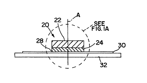
FIG. 1A shows an enlarged side view of the EMI gasket assembly 20,
reflecting a preferred embodiment of the invention. Specifically, the EMI
gasket
assembly 20 comprises an electrically conductive gasket material 22, an
electrically conductive solderable support layer 24, means (adhesive 26) for
is affixing the electrically conductive gasket material 22 to the support
layer 24,
and a solder layer 28 which secures the entire assembly to a conductive
surface, such as a ground trace 30 of a PCB 32 (see FIGS. 1 and 7 which
illustrate PCB 32}. One type of electrically conductive gasket material which
may be particularly suited for use with the present invention is GORE-SHIELD~
2o brand EMI gasket material type GS500, GS3000 or GS5200, available from W.
L. Gore & Associates, Inc. of Newark, Delaware. Other suitable electrically
conductive gasket materials will be described in greater detail below.
As the term is used herein "solderable" shall mean capable of fusing,
joining, or metallurgically bonding with solder to form an electrically
conductive
25 joint, connection or interface.
The electrically conductive gasket material 22 may be rectangular in
cross section (from the side) as shown; however, it may also be round, oval,
pointed, curled, etc. Such other cross sections of the gasket 22 are
illustrated
in FIGS. 2-5, wherein FIG. 2 illustrates a rectangular cross section, FIG. 3 a
3o triangular cross section, FIG. 4 a curved or crescent-shaped cross-section
and
FIG. 5 a half-rounded- and half-rectangular-shaped cross section. Sometimes,
the electrically conductive gasket shape is deliberately formed to achieve a
desired result, such as to decrease the required force to compress the EMI
gasket material with a shield (not shown). This allows for smaller screws or
CA 02325141 2000-09-20
WO 99!51074 PCT/US99/03577
_.g_
even snaps to fasten the shield to the PCB 32.
It should be noted that suitable means for affixing metal support layer 24
to the electrically conductive gasket material 22 include, but are not limited
to,
non-conductive adhesive, electrically conductive adhesive, molding, or
mechanical means, such as a barb assembly or retention clips.
In instances where the adhesive 26 is employed, any suitable adhesive
may be used to attach or affix the electrically conductive gasket material 22
to
the support layer 24, as long as an electrical path is maintained
therebetween.
In one embodiment, a particle filled electrically-conductive pressure-
sensitive
to acrylic adhesive may be used. This adhesive is laminated to the gasket in
transfer-roll form, but it may be directly applied to the gasket; or applied
in
some other form. In fact, the adhesive itself is not necessary for affixing
the
gasket to the support layer. The invention only requires some means to
electrically and mechanically connect the gasket to the support layer. An
electrically-conductive, pressure-sensitive adhesive is one exemplary way of
achieving this attachment; however, the adhesive could also be thermoset,
thermoplastic, etc. Also, the adhesive might not need to be electrically-
conductive if the support layer 24 can be made to mechanically touch the
gasket 22 in some areas to keep an electrical path along a z-axis "A". (FIGS.
1-3.) Additionally, the electrically conductive gasket material 22 could be
directly molded to the support material or mechanically fastened in some other
manner (such as with support barbs, etc.), thus eliminating the need for an
adhesive 26 altogether. Whatever the case, the fastening means must be able
to withstand solder reflow temperatures and retain its mechanical and
electrical
properties.
The support layer 24 should impart sufficient stiffness to the electrically
conductive gasket material 22 to permit the assembly to be effectively
processed with SMT machines. Thus, the support layer 24 may be made of a
variety of different materials, such as plastic or metal; however if it is
plastic, it
3o must be plated with a solderable metal such as copper, nickel, gold,
silver, tin,
etc. If the support layer 24 is metal, it should be easily solderable, or
plated
with a similar metal such as described above. Gold, nickel and tin are
preferred plating materials, and are used extensively in the industry. Also,
the
support layer 24 may be any thickness, especially if it is desired to fill an
CA 02325141 2000-09-20
WO 99/51074 PCTNS99/03577
_g_
existing gap in a design. Thus, the gasket 22 thickness can be kept to a
standard thickness, white modifying the support layer 24 thickness to
accommodate different designs. Also, the support layer 24 does not need to
be rectangular in cross-section, as would occur if the part was stamped or cut
from a sheet metal material. For example, the support layer 24 can be molded
into a trapezoidal shape, parallelogram, etc., depending upon the application:
Whatever material the support layer 24 is fabricated from, it must be able to
withstand solder reflow temperatures.
FIG. 6 illustrates an example of an EMI gasket assembly 20
to contemplated by the instant invention. FIG. 7 shows a typical PCB 32, with
several gasket assemblies 20 installed at various locations on ground traces
30. The assembly 20 is dimensioned as shown for illustration purposes only,
accordingly assembly 20 can readily be made wider, thicker, longer, thinner,
etc., depending upon an application. In the case shown in FIG. 7, the
is assemblies 20 are hypothetically shown to be installed strategically in
desired
locations.
Referring now to FIGS. 8 and 9, FIG. 8 shows a typical section of tape
and reel 36, used to feed the EMi gasket assembly 20 into an SMT machine.
The assemblies 20 are received in pockets 38, which are positioned to allow a
2o vacuum head 40 (FIG. 9) of an SMT machine (not shown) to easily and
precisely access and pick up the assemblies 20 from their respective pockets
38 for placement. This process is illustrated in FIG. 9, which reveals a
cutaway
view of the vacuum head 40 on the SMT machine, holding a gasket assembly
20 ready for installation. The ground trace 30, in FIG. 9, has already been
2s prepared with a screened pattern of solder paste 28, to mate with the
support
layer 24 of the assembly 20. Once assembly 20 is deposited on ground trace
30, the solder is reflowed by any suitable means, such as a solder refiow
oven,
for example.
FIGS. 10-12 reveal a pair of alternate embodiments of the present
3o invention. As shown therein, support layer 24 is extended to act as a
spring-
like finger 42, which gives an improved metal-to-metal configuration. This
extra
contact of the support layer 24 provides lower resistance for the entire
assembly 20 than without it, since the metal or plating typically have better
conductivity than the electrically conductive gasket 22 material. Used in this
CA 02325141 2003-10-09
WO 99/51074 . PCT/US99l03577
r ' -10-
configuration, the assembly 20 is able to give improved performance over an
assembly without the extra contacts. in the drawing figures, one embodiment
(FIG. 10) shows a pair of spring fingers 42, folded over at the ends, while
the
other embodiment (illustrated in FIGS. 11 and 12) reveals a single forger 42
at
the center. Other configurations similar to the ones iNustrated in FIGS. 10-12
are further contemplated.
Lastly, FIG. 13 shows a set of five EMI gasket assemblies 20, of varying
thicknesses, used in combination. This configuration might be used to combat
flexing in a mating shield, which tends to bow away from the PCB 32 between
io housing fastening locations. This can_give improved performance over a.set
of
gasket assemblies with identical thicknesses.
As~stated hereinabove, any suitable electrically conductive material may
be used in the construction of an SMT compatible EMI gasket 20 in accordance
with the teachings of the present invention. The embodiments of suitable
i5 conductive gasket material provided hereinbelow ace provided for purposes
of
illustration only, and are not intended to limit the scope of the present
invention.
ELECTRICALLY CONDUCTIVE GASKET MATER~I~LS
A first suitable electrically conductive gasket material 22 may be~
2o fabricated from an electrically conductive polymer matrix of the type
described
in detail in United States Patent No. 5,431,571.
A second suitable electrically conductive gasket material 22 may be
fabricated from an electrically conductive gasket material of the type
described
25 in detail in United States Patent No. 5,286,568"
A third suitable electrically conductive gasket material 22 may be
fabricated from material of the type described in detail in United States
Patent
No. 5,604,026.
so A fourth suitable electrit;alty conductive gasket material 22 may be an
electrically conductive polytetrafluoroethytene .(PTFE) article which has an
expandable particulate blended into a PTFE and conductive metal composition.
Spec~cally, the expandable particulate exhibits intumescence upon application
of heat. The expandable particulate is not homogeneous, ~i.e., it is, not a
CA 02325141 2000-09-20
WO 99/51074 PCT/US99/03577
-11-
polymeric bead, but rather comprises a polymeric shell having a central core
comprised of a fluid material. A further characteristic is that the overall
dimensions of the expandable particulate increase upon heating at a specific
temperature.
Expandable hollow polymeric particulate which is useful includes those
materials comprised of a polymeric shell and a core of at least one other
material, either liquid or gaseous, most preferably a liquid at room
temperature,
in which the polymeric shell is essentially insoluble. A liquid core is
advantageous because the degree of expansion is directly related to the
to volume change of the core material at the expansion temperature. For a
gaseous core material, the volume expansion expected can be approximated
from the general gas laws. However, expandable particulate comprising a
liquid core material offers the opportunity to provide much larger volume
changes, especially in those cases where a phase change takes place (i.e., the
liquid volatilizes at or near the expansion temperature).
Preferred expandable polymeric particulate (also called microspheres,
microbalioons, and microbubbles) can have shells comprising copolymers such
as vinyl chloride and vinylidene chloride, copolymers of vinyl chloride and
acrylonitrile, copolymers of vinylidene chloride and acrylonitrile, copolymers
of
2o methacrylonitriie and acrylonitrile, and copolymers of styrene and
acrylonitrile.
Further materials worth mentioning are copolymers of methyl methacrylate
containing up to about two percent by weight of styrene, copolymers of methyl
methacrylate and up to about 50 percent by weight of ethyl methacrylate, and
copolymers of methyl methacrylate and up to about 70 percent by weight of
orthochlorostyrene. The unexpanded microspheres contain fluid, preferably
volatile liquid, i.e., a blowing agent, which is conventional for microspheres
of
the type described here. Suitably, the blowing agent is 5 percent to 30
percent
by weight of the microsphere. The microspheres can be added in different
manners, as dried particles, wet cakes, or in a suspension, e.g., in an
alcohol
3o such as isopropanol.
Unexpanded particulate desirably is in the size range of from about 0.1
micrometer to about 600 micrometers, preferably from 0.5 micrometer to 200
micrometers, and most preferably from 1 micrometer to 100 micrometers.
Expanded particulate can have a size in the range of from about 0.12
CA 02325141 2003-10-09
WO 99/51074 PCT/US99/03577
-12-
micrometer to 1000 micrometers, preferably from 1 micrometer to fi00
micrometers. After expansion, the volume of the expandable particulate
increases by a factor of at least 1.5, preferably by a factor of at least 5,
and
most preferably by a factor of at least 10, and may even be as high as a
factor
5 of about 100.
Suitable microspheres are commercially available from Nobel Industries
of Sundsvall, Sweden, under the trademark EXPANCEL~. These
microspheres may be obtained in a variety of sizes and forms, with expansion
temperatures generally ranging from 80°C to 130°C. A typical
EXPANCEL~
io microsphere has an initial average diameter of 9 to 17 micrometers and an
average expanded diameter of 40 to 60 micrometers. According to Nobel
Industries, the microspheres have an unexpanded true density of 1250-1300
kglm', and an expanded density below 20 kg/m'.
It should be understood that the use of the term "energy expandable
i 5 particulate" herein is intended to encompass any hollow resilient
container filled
with volatile fluid which, is adapted, to expand. Although presently available
microspheres are essentially ball-shaped particles adapted to expand when
exposed to an energy source, it should be understood that such microspheres
are quite resilient in their expanded form and can tie compressed and released
.
20 (e.g., through extrusion) to achieve the expansion required for the present
invention. Additionally, it may be possible to form such products in a variety
of
other shapes, such as tubes, ellipsoids, cubes, particles, etc. As such, the
term '.'energy expandable particulate° is intended to include all
applicable forms
and usas of these products now known or later developed.
25 A wide variety of blowing or raising agents may be enclosed within the
polymeric shell of the expandable microspheres. They can be volatile fluid
. forming agents such as aliphatic hydrocarbons including ethane, ethylene;
propane, butane, isobutane, isopentane, neopentane, acetylene, hexane,
heptane, or mixtures of one or more such aliphatic hydrocarbons, preferably
3o having a number average molecular weight of at feast 28, and a boiling
point at
atmospheric pressure about the same temperature range or below the range of
the softening point of the resinous material of the polymeric shell when
saturated with the particular blowing agent utilized.
CA 02325141 2003-10-09
WO 99!51074 ~ PCTNS99l03577
-13-
EXPANCEL~-type 091 ~U microspheres may be employed. This product
comprises an off-white dry powder with a particle size ranging between 10 and
40 micrometers. The shell of these microspheres comprise acrylonitriie
whereas the volatile liquid comprises isopentane.
It has been found that by mixing a dry preparation of EXPANCEL~
microspheres with a dispersion of PTFE, or similar polymer, and then heating
the resulting composition, the polymer will undergo expansion in three- '
dimensions to achieve a fibrillated PTFE matrix.
In accordance with this embodiment, a precursor material comprised of:
to electrically conductive particulate; PTFE, in the form of paste, dispersion
or
powder; and microspheres, in the form of a dry powder or solution, is mixed in
proportions of at least 20 to 90 volume percent conductive particulate, 3 to
15
volume percent EXPANCEL~ mierospheres,~ and 5 to 70 volume percent
PTFE, with proportions of 60 volume percent conductive particulate, 6 volume
i5 percent EXPANCEL~ microspheres and 34 volume percent PTFE being
preferred in an embodiment comprising at least in part electrically conductive
flakes. Mixture may occur by any suitable means, including dry blending of
powders, wet blending, co-coagulation of aqueous dispersions and slurry
filler,
high shear mixing, etc. As the term is used herein, "volume percent" shall
2o mean a percentage of the volume of the precursor material.
Electrically conductive particulate enmeshed within the resulting PTFE
precursor material is the major component thereof. The electrically conductive
particulate may include, but is not limited to, metal powder, metal bead,
metal
fiber, or metal flake, or 'tt can be a metal coated particulate such as metal
z 5 coated metals, metal coated ceramics, metal coated glass bubbles, metal
coated glass beads, or metal coated mica flakes. Preferred conductive metals
in particulate form include, but are not limited to silver, nickel, aluminum,
copper, stainless steel, graphite, carbon, gold, or platinum, for example.
Preferred metal coatings inGude silver, nickel, copper, or gold. Additionally,
a
3 o combination of two or more conductive particulates can be used. Average
sae
of the conductive flakes can be from about 1 Nm to about 200 Irm, ,
preferably from about 1 Nm to about 100 Nm, and most preferably from
about 20 um to about 40 Nm. Average size for conductive powders can
be from about 0.5 Nm to about 200 Nm, preferably from about 0.5 Nm to
. .__._..~ ....._ _ __ ~__ _ ._ .
CA 02325141 2003-10-09
WO 99/51074 PC'TNS99103577
-14-
about 100 pm, and most preferably from about 2 Nm to about 60 Nm.
,The PTFE aqueous dispersion employed in producing the PTFE
precursor of the present embodiment can be a milky-white aqueous suspension
of PTFE particles. Typically, the PTFE aqueous dispersion will contain about
20 percent to about 70 percent by weight solids, the major portion of such
solids being PTFE particles having a particle size in the range of from 0.05
micrometers to about 5.0 micrometers. Such PTFE aqueous dispersions are
presently commercially available from the E. I. duPont de Nemours Company,
for example, under the tradename TEFLON~ 3636, which is 18 percent to 24
i o percent by weight solids being for the most part PTFE particles of about
0.05
micrometers to about 5.0 micrometers. A thickness of the above described
precursor material may'range from about 5 mils to about 125 mils, for example.
Upon heating the precursor material, thickness increases due to the
expansion of the energy expandable particulate. The amount of expansion
i s observed is dependent on several factors, including the weight percent of
energy expandable particulate present, the type of energy expandable
particulate, the molecular weight of the polymeric shell of the energy
expandable particulate, and the toughness of the PTFE matrix holding the
precursor material together. Typical thickness of the material of this
2 o embodiment can be in the range of from about at least 10 mits, and
preferably
from 10 to 100 mils, and most preferably from 20 to 60 mils. Other thicknesses
can be achieved.
Temperatures needed for the thertnal.expansion step to occur are
dependent on the type of polymer comprising the shell of the microsphere and
2 s . on the particular blowing agent used. Typical temperatures range from
about
40°C to about 220°C, preferably from 60°C to
200°C, most preferably
from 80'C to 190'C.
(n addition to the comppsite article which has been described above, an
alternate embodiment may be made by adding an elastomer material, such as
so a silicone elastomer material (e.g., dimethyl siloxane) to the precursor
material.
In one embodiment of the present invention, this is achieved by compounding
the filled fine powder coagulum with the dimethyl siloxane. A suitable
dimethyl
siloxane is Syigard~ type 1-4105, or Q1-4010, which may be obtained from
Dow Coming. tt may also be suitable to use a silicone dioxide reinforced
CA 02325141 2003-10-09
WO 99!51074 PCT/U599/03577
-15-
silicone material such as Q3-661, which may also be obtained from Dow
Coming. The siloxane is added on a weight per weight basis, and may be
diluted with a solvent, such as mineral spirits, for example. In general, the-
siloxane may be added in amounts ranging from 1 percent to about 50 percent,
s preferably from 5 percent to about 20 percent, and most preferably from 14
percent to about 15 percent. Qther suitable elastomer materials include, but
are not limited to, silicone rubbers, fluorosilicone elastomers, fluorocarbon
elastomers, perfluoro elastomers, other fluoroelastomer materials, or
polyureathane.
1o Subsequently, this precursor material is heated in a range from about
130°C to about 190°C, to not only achieve expansion of the
precursor
material, but also to catalyze the siloxane into a cured state. The resulting
article is an easily compressible, continuously electrically conductive PTFE
composite, including a silicone elastomer disposed within the composite
article
is in a discontinuous fashion.
The addition of the elastomer material yields a composite with increased
z-axis strength, tensile strength and elongation. it also provides some degree
of resilience and increases the usable temperature range of the material.
These desired properties are achieved without sacrifiang electrical
conductivity
20 or softness/compressibility of the composite article.
An electrically conductive gasket material fabricated from an
elastomer impregnated with a material selected from a group consisting
of silver, nickel, silver-plated copper, silver-coated glass, nickel-graphite,
and carbon, is suitable.
2s A fifth suitable electrically conductive gasket material 22 includes an
electrically conductive polytetrafluoroethylene (PTFE) article which has an
elastomer material and electrically conductive particles intermixed therein.
Specifically, the conductive gasket material of this embodiment is defined by
a
plurafdy of electrically conductive particles and PTFE in the forth of paste,
30 , dispersion or powder. The electrically conductive particles and PTFE are
mixed in proportions to achieve a mixture containing about 50 to 90 volume
percent electrically conductive particles. Mixture may occur by any suitable
means, including dry blending of powders, wet blending, co-coagulation of
......_.a_..~.--..~...
CA 02325141 2003-10-09
WO 99/51074 PCT/US99J03577
-16-
aqueous dispersions and slurry filler, or high shear mixing, for example. As
the
term is used herein, "volume percent" shall mean a percentage of the total
volume of a material or mixture.
Electrically conductive particles enmeshed within the resulting composite
I is a major component thereof. The electrically conductive particles may
include, but are not limited to,,metal powder, metal bead, metal fiber, or
metal
flake, or the particles may be defined by a metal coated particulate such as
metal coated metals, metal coated ceramics, metal coated glass bubbles, metal
coated glass beads, or metal coated mica flakes. Preferred conductive
lo materials in particulate form include, but are not limited to, silver,
nickel,
aluminum, copper, stainless steel, graphite, carbon, gold, or platinum, for
example. Preferred metal coatings include silver, nickel, copper, or gold.
Additionally; a combination or mixture of two or more of the foregoing may be
employed. Average size of the conductive flakes can be from about 1 lrm
to about 200 Nm, preferably from about 1 ~m to about 100 um, and most
preferably from about 20 Irm to about 40 Nm. Average size for
conductive powders can be from about 0.5 Nm to about 200 Irm, arid
most preferablyfrom about 2 pm to about 100 Nm.
The PTFE aqueous dispersion employed in producing the electrically
2o conductive composite article of this embodiment maybe a milky-white aqueous
suspension of PTFE particles. Typically, the PTFE aqueous dispersion will
contain about 20 percent to about 70 percent by weight solids, the major
portion of such solids being PTFE particles having a particle size in a range
from about 0.05 micrometers to about 5.0 micrometers. Such PTFE aqueous
2s dispersions are presently commercially available from the E. l, duPont de
hlemours Company, for example, under the tradename TEFI.ON~ 3636, which
is 18 percent to 24 percent by weight solids being for the most part PTFE
particles of about 0.05 micrometers to about 5.0 micrometers.
An elastomer material, such as a silicone elastomer material (e.g.,
3 o dimethyl siloxane), is disposed within the conductive gasket material.
This is
achieved by compounding a filled fine powder coagulum of PTFE and
electrically conductive particles with the elastomer material. A suitable
dimethyl
CA 02325141 2003-10-09
WO 99/51074 PCT/US99/03577
-17-
siloxane is Sylgard~ type 1-4105, or Q1-4010, which may be obtained from
Oow Coming. (It may also be suitable to use a silicone dioxide reinforced
silicone material such as Q3-681, which may also be obtained from Dow
Coming.)
The elastomer material, such as the dimethyl siloxane, is added on a
weight per weight basis, and may be diluted with a solvent, such as mineral
. spirits, for example. In general, the elastomer material may be added in
amounts ranging from about 1 percent to about 75 percent, preferably from
about 5 percent to about 20 percent, and most preferably from about 10
1o percent to about 15 percent. Other suitable elastomer materials include,
but are
not limited to; silicone rubbers, fluorosiiicone elastomers, fluorocarbon
elastomers, perfluoro elastomers, fluoroelastomers, polyurethane, or
ethylenelpropylene (EPDM).
Subsequent to the addition of the elastomer material, the composite
15 article is heated in a range from about 130'C to about 190°C, to
catalyze the
elastomer material into a cured state. The resulting composite article is a
continuously electrically conductive composite article having a main body
which
may be dimensioned into any suitable shape or thickness.
The addition of the eiastomer material yields a continuously electrically
2o conductive composite article with an increased z-axis strength and tensile
strength. The elastomer also provides some degree of resilience. These
desired properties are achieved without saucing electrical conductivity.
An electrically conductive gasket rnaterial fabricated from an
elastomer impregnated with a material selected from a group consisting of
25 silver, nickel, silver-plated copper, silver-coated glass, nickel-
graphite', and
carbon, is suitable.
Although a ~w~eXemplary embodiments of the present invention have
been described in detail above, those skilled in the art readily appreciate
that
many modifications are possible without materially departing from the novel
30 teachings and advantages which are described herein. Accordingly, all such
modifications are intended to be included within the scope of the present
invention, as defined by the following claims.