Note: Descriptions are shown in the official language in which they were submitted.
CA 02325956 2000-09-25
WO 99/49352 PCT/US99105933
TAB AND BATS BAR APPLICATION METHOD
FIELD OF TSE INVENTION
This invention relates to a method for applying a
conductive epoxy-based electrical contact system to a
substrate, and to the resulting metallized substrate. A
preferred embodiment involves applying a conductive epoxy bus
bar/tab system to an optical substrate, such as an ophthalmic
lens. The instant method is particularly useful in preparing
electrooptic devices, such as electrochromic lenses.
BACKGROQND OF TH8 ART
The transmittance properties of electrochromic
materials change in response to electrically driven changes in
oxidation state. Thus, when an applied voltage from an
external power supply causes electrons to flow to (reduction)
or from (oxidation) an electrochromic material, its
transmittance properties change. In order to maintain charge
neutrality, a charge balancing flow of ions in the
electrochromic device is needed. By enabling the required
electron and ion flows to occur, an electrochromic device
facilitates reversible oxidation and reduction reactions
during optical switching.
Conventional electrochromic cells comprise at least
one thin film of a persistent electrochromic material, i.e. a
material responsive to the application of an electric field of
a given polarity to change from a high-transmittance, non-
absorbing state to a low-transmittance, absorbing or
reflecting state. Since the degree of optical modulation is
directly proportional to the current flow induced by an
applied voltage, electrochromic devices demonstrate light
transmission tenability between high-transmittance and low-
CA 02325956 2000-09-25
WO 99/49352 PCT/US99/05933
- 2 -
transmittance states. In addition, these devices exhibit
long-term retention of a chosen optical state, requiring no
power consumption to maintain that optical state. Optical
switching occurs when an electric field of reversed polarity
is applied.
To facilitate the aforementioned ion and electron
flows, at least one electrochromic film which is both an ionic
and electronic conductor is in ion-conductive contact,
preferably direct physical contact, with an ion-conducting
material layer. The ion-conducting material may be inorganic
or organic, solid, liquid or gel, and is preferably an organic
polymer. The electrochromic films) and ion-conductive
material are disposed between two electrodes, forming a
laminated cell. As voltage is applied across the electrodes,
ions are conducted through the ion-conducting material.
When the electrode adjacent to the electrochromic
film is the cathode, application of an electric field causes
darkening of the film. Reversing the polarity causes reversal
of the electrochromic properties, and the film reverts to its
high-transmittance state. Typically, an electrochromic film
such as tungsten oxide is deposited on a substrate coated with
an electroconductive film such as tin oxide or indium tin
oxide to form one electrode. The counter electrode is
typically a similar tin oxide or indium tin oxide coated
substrate. A complimentary electrochromic film, for example
an iridium oxide film, can also be used.
An electrochromic device; such as an electrochromic
lens, also requires a means for delivering electrical current
from a power source to each of its electrodes. This can be
accomplished via use of a bus bar, as disclosed in U.S. Pat.
Nos. 5,520,851 and 5,618,390 to Yu, et al.
CA 02325956 2000-09-25
WO 99/49352 PCT/US99/05933
- 3 -
U.S. Pat. No. 3,630,603 to Letter discloses an
electrochromic eyewear control circuit. U.S. Pat. No.
4,991,951 to Mizuno discloses metal eyeglass frames used in
conjunction with electrooptic lenses.
U.S. Pat. No. 4,335,938 to Giglia discloses
electrochromic devices having a layer of tungsten oxide in
contact with a layer of organic electrolyte resin comprising a
hydrophilic layer of 2-acrylamido-2-methylpropanesulfonic acid
homopolymer and an electrode means for changing electrochromic
properties of the device.
U.S. pat. No. 5,327,281 to Cogan discloses the use
of epoxy to seal a cavity formed when a spacer is used to
separate electrodes and contains a liquid electrolyte injected
between the spaced electrodes.
U.S. Pat. No. 5,656,150 to Kallman, et al.,
discloses electrochromic devices and the use of contacts
connecting first and second electrodes to flex circuits or
other means of wiring.
2 0 StJI~ARY OF THE INVENTION
This invention is directed to a method for applying
bus bar/tab systems to various substrates and to the resulting
metallized substrates. More narticulari~_ rh;~ mer~,~a
involves applying a conductive epoxy bus bar and a tab to a
substrate, said substrate having a peripheral edge region
situated between first and second expanse surfaces, in a
manner which provides reliable electrical contact between the
tab and bus bar, and which allows the.bus bar and tab to be
used as electrical conduits between a power source and an
electrode. For example, in electrooptic applications, a
conductive epoxy bus bar is applied to the peripheral edge
region of an optical substrate having or which will have an
CA 02325956 2000-09-25
WO 99/49352 PCT/US99/05933
- 4 -
electroconductive film on an adjacent expanse surface. The
conductive epoxy and electroconductive film are disposed so as
to overlap at or near the interface of the peripheral edge
region and the expanse surface. The connecting portion of a
tab, preferably its connecting end, is embedded in the
conductive epoxy. Curing of the epoxy firmly connects the tab
to the epoxy bus bar, which, in conjunction with suitable
circuitry, facilitates delivery of current from a power source
through the tab and the conductive epoxy bus bar to the
electroconductive film.
As used herein, the term bus bar' refers to a
strip, coating or band of low resistance electrically
conductive epoxy that is applied to a substrate. A bus bar is
generally positioned so that it is in contact with or will
contact an electroconductive material disposed on the
substrate. Further, the term ~tab~ refers to a conductive
Wire or strip which links or connects a bus bar to a power
source through an electrical circuit, for example an
electrooptic or electrochromic control circuit. A tab can
either be an integral part or a separate component of such a
circuit. A tab is generally affixed to a bus bar at a
connecting end, though this invention contemplates tab
connection along any portion of its surface.
A bus bar preferably is applied to the peripheral
edge region of a substrate having or which will have a metal
or metal oxide electroconductive film (e. g., fluorine-doped
tin oxide, tin-doped indium oxide, antimony-doped tin oxide,
aluminum-doped zinc oxide, etc.) on an adjacent expanse
surface (hereinafter referred to as an electroconductive
expanse surface). Electrical contact between the bus bar and
an electroconductive film is preferably made at the interface
of the peripheral edge region and an electroconductive expanse
CA 02325956 2000-09-25
WO 99/49352 PCT/US99/05933
- 5 -
surface of a given substrate by causing the electroconductive
film on the expanse surface to overlap the bus bar, or vice
versa. It is desirable that a bus bar have a lower electrical
resistance than the electroconductive film that it contacts.
For example, bus bar sheet resistances of less than 20
ohms/sq. are preferred when electroconductive films having
sheet resistances of 20-25 ohms/sq. are used.
In a preferred embodiment, a bus bar is applied to
the peripheral edge region of a shaped substrate. As used
herein, the term shaped substrate refers to a substrate
prepared by grinding or cutting the perimeter of an oversized
blank substrate to a smaller size having a desired shape.
This grinding process is.commonly referred to as edging. For
ophthalmic lenses, disk-shaped, oversized blank lenses are
edged to shape via conventional techniques well known to
skilled practitioners. The bus bar on such a shaped lens is
usually confined to its peripheral edge region so that it is
unobtrusive.
Bus bar dimensions are generally determined by
resistance requirements and the shape of the electroconductive
film that a given bus bar contacts. Thus, a bus bar can cover
the full peripheral edge region of a substrate or it can be
limited to some portion thereof. To avoid application of
conductive epoxy beyond the targeted surface of a given
substrate, the substrate can be mechanically masked so that
only the desired bus bar target surface is exposed during bus
bar application. It is also desirable that a bus bar adhere
strongly to the substrate to which it is applied.
In a preferred embodiment involving applying a
conductive epoxy bus bar/tab system to an ophthalmic lens, the
edge region of a blank lens is first ground to shape via a
conventional edging technique. A bus bar is then added by
CA 02325956 2000-09-25
WO 99/49352 PCT/US99/05933
- 6 -
applying a curable conductive epoxy layer to the peripheral
edge region of the shaped lens by a suitable application
means, with masking as needed.
After or during application of the curable
conductive epoxy layer to the bus bar target area of a given
substrate, a tab is connected to the epoxy layer by embedding
a portion of the tab, preferably a connecting end, in the
epoxy layer. As used herein, the term ~embed~ refers to
placing, inserting or fixing a connecting portion of a tab in
l0 a conductive epoxy layer or between conductive epoxy layers so
as to substantially surround the connecting portion of the tab
with conductive epoxy. The tab can be embedded by various
means, including inserting the connecting portion of the tab
into a curable conductive epoxy layer prior to or during
curing (i.e., while the epoxy is soft or pliable), placing the
connecting portion of the tab onto an outer surface of an
uncured, partially or fully cured conductive epoxy layer, and
then placing additional curable conductive epoxy over the
connecting portion, or placing the connecting portion of the
tab onto the bus bar target area of the substrate, with or
without the use of an attachment means (e. g., a structural
epoxy, conductive epoxy or other adhesive) and then applying a
curable conductive epoxy layer over the connecting portion of
the tab. Curing of the conductive epoxy then secures the tab
to the bus bar.
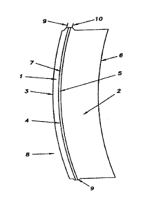
One embodiment of the electrical contact system of
this invention is illustrated in the Figures. As shown in
Figures 3 and 4, the connecting ends of tabs 9 and 10 are
embedded in conductive epoxy bus bars 11 and 12, respectively,
which in turn are positioned on the top peripheral edge
regions of shaped front and rear lenses 1 and 2. Shaped
CA 02325956 2000-09-25
WO 99/49352 PCT/(JS99/05933
Lenses 1 and 2 are laminated to form electrochromic lens 8, as
shown in Figures 1 and 2.
BRIEF DESCRIPTION OF THE DRAwINC3S
Figure 1 is a side view of a laminated
electrochromic lens showing front and rear lens tabs.
Figure 2 is a front view of the laminated lens of
Figure 1 showing bus bar and tab orientation.
Figure 3 is a cross-sectional blow-up of the front
tab and bus bar of the lens shown in Figure 1.
Figure 4 is a cross-sectional blow-up of the rear
tab and bus bar of the lens shown in Figure 1.
DETAILED D88CRIPTION OF THE INVENTION
Other than in the operating Examples, or where
otherwise indicated, all numbers quantifying ingredients,
amounts, dimensions, ratios, ranges, reaction conditions,
etc., used herein are to be understood as modified in all
instances by the term 'about'.
In its broadest sense, the instant invention is
directed to a method for applying or affixing a conductive
epoxy bus bar/tab system to a substrate, said system
comprising a cured conductive epoxy layer and a tab having a
connecting portion or end, wherein said connecting portion or
end is embedded in said cured conductive epoxy layer, which
method comprises: a) embedding the connecting portion of said
tab in a curable conductive epoxy layer applied to a bus bar
target area on said substrate, preferably to a target area on
the peripheral edge region of said substrate; and b) curing
said curable conductive epoxy. This method connects a tab to
a conductive epoxy bus bar positioned on a given substrate,
thereby establishing electrical contact between the tab and
CA 02325956 2000-09-25
WO 99/49352 PGT/US99105933
- 8 -
bus bar. Preferably, a tab is affixed by embedding one of its
ends, i.e., its connecting end, in a conductive epoxy bus bar.
In preferred embodiments of this method, the
connecting end or portion of a tab is inserted into a curable
(i.e., uncured or partially cured) conductive epoxy layer
while the layer is pliable enough to allow insertion. Curing
of the curable epoxy layer then secures the tab to the bus
bar. Alternatively, the connecting end or portion of a tab is
placed on a first conductive epoxy layer, said epoxy layer
being in a curable (i.e., an uncured or partially cured) or
cured state. Additional curable conductive epoxy (i.e., a
second conductive epoxy layer) is then applied over the
connecting end or portion of the tab, and all curable
conductive epoxy layers are permitted to cure. These
techniques embed the connecting end or portion of a tab in a
single- or multi-layered conductive epoxy bus bar.
In another embodiment of the instant method, the
connecting end or portion of a tab is placed on or affixed to
the bus bar target area of a substrate, and a curable
conductive epoxy layer is applied over the end or portion of
the tab in contact with the substrate. Curing of the curable
conductive epoxy layer establishes electrical contact between
the tab and the resulting conductive epoxy bus bar. A
structural epoxy, conductive epoxy or other adhesive, with
appropriate curing, can be used to affix the tab to the
substrate, if desired. In each of these embodiments,
conductive epoxy embeds or substantially surrounds the
connecting portion or end of a tab. Additional methods of
embedding may become apparent to skilled artisans.
The instant invention is also directed to a
substrate having a conductive epoxy bus bar and tab affixed
thereto via any of the instant methods. Such substrates,
CA 02325956 2000-09-25
WO 99/49352 PGT/US99105933
_ g _
which are preferably shaped substrates, can be used to prepare
single stack electrooptic or electrochromic devices, wherein
electrodes, electrochromic materials) and possibly an ion-
conducting material are coated as a stack on a first substrate
which may or may not be laminated to a second substrate, and
to prepare laminated electrooptic or electrochromic devices
wherein first and second electrodes are coated on first and
second substrates, respectively, each of which contains a bus
bar. Multiple bus bars can be applied to a single substrate,
if necessary. Preferred substrates are optical lenses; more
preferred substrates are ophthalmic substrates.
Any curable conductive epoxy which adheres to and is
compatible with the substrate being treated, which has
workable cure characteristics (i.e., cure time, cure
temperature, etc.) and which has suitable electrical
conductivity properties can be used to form a conductive epoxy
bus bar via the instant method. For example, commercially
available silver epoxies, nickel epoxies, chromium epoxies,
gold epoxies, tungsten epoxies, alloy epoxies and combinations
thereof can be used as conductive epoxy bus bar materials.
Preferred conductive epoxies are Tra-Duct~ 2902 silver epoxy
and Applied Technologies 5933 alloy epoxy, which are
commercially available from Tra-Con, Inc., and Applied
Technologies, respectively.
An effective amount of curable conductive epoxy is
applied. This means that the curable conductive epoxy applied
to a given substrate is of sufficient thickness and coverage
to fully coat the bus bar target area of that substrate and to
provide the desired resistivity. Conductive epoxy bus bars
can be applied by any suitable means, for example, by brush,
extrusion, roller, etc. Such coating means are well known to
skilled practitioners. Preferred conductive epoxy bus bars
CA 02325956 2000-09-25
WO 99/49352 PCT/US99/05933
- 10 -
are generally 2 to 50 mils thick, and extend around a
substantial portion or all of the peripheral edge region~to
which they are applied.
The instant curable conductive epoxies usually
comprise resin and harder components. These components are
mixed prior to application in accordance with the relevant
manufacturer s instructions. Curing is also preferably
accomplished in accordance with manufacturer s instructions.
Suitable conductive epoxies have cure times ranging from a few
l0 minutes to a few hours. An effective cure time is the time
required for a given epoxy to cure to the extent that it
becomes rigid enough to secure the connecting end or portion
of a tab and develops sufficient electrical conductivity.
In a preferred embodiment, a curable conductive
epoxy bus bar is applied to the peripheral edge region of a
shaped substrate, i.e., a substrate which has been edged to
shape using conventional edging/grinding techniques. The
cross-sectional profile of the peripheral edge region to which
a conductive epoxy bus bar is applied is not believed to be
critical; the edge region profile can be, for example, flat,
V-shaped, U-shaped, mesa shaped, square shaped, rounded or
irregularly shaped. It is, however, desirable to avoid sharp
edges in some applications, as they tend to concentrate
stress. A particularly preferred embodiment requires that a
blank substrate be edged to form a rounded or sloped
transition zone between its peripheral edge region and its
electroconductive expanse surface. Such a zone facilitates
contact between an electroconductive film and a conductive
epoxy bus bar.
After and/or during application of a curable
conductive epoxy layer to a bus bar target area, a tab is
embedded into the curable conductive epoxy. Tab location is
CA 02325956 2000-09-25
WO 99/49352 , PCTNS99/05933
- 11 -
not believed to be critical. Preferably, tabs are located so
as to readily connect with corresponding circuitry. It is
also preferred that the connecting end or portion of a tab be
barbed, t-shaped, or otherwise irregularly shaped to help to
secure the tab to the bus bar during the embedding step.
Any suitable wire or metal strip can be used as a
tab. Preferably, a tab is sufficiently rigid to allow
insertion into a pliable conductive epoxy layer, yet strong
and pliable enough to be bent, shaped and/or connected to a
l0 circuit without breaking. Typical wire materials include, but
are not limited to, nickel, silver, titanium, gold, platinum
and copper. Such Wires are commercially available from
Aldrich, Inc., at 99.9% purity, by weight. Stainless steel
tabs can also be used. Tab dimensions are not critical, and
should be based on available space (e. g., the peripheral edge
region width for a particular device) and resistance
specifications. Generally, for electrochromic applications,
wire resistances of less than about 2 S~ across a 2 inch (5 cm)
length are desired. Tab thickness generally ranges between
0.5 and 5 mils. If strips are used instead of wires, widths
between 20 and 50 mils are typical.
Though the instant tab/bus bar application method is
applicable to virtually any substrate, the preferred
substrates of the instant invention are glass or organic
polymeric substrates conventionally used to prepare optical
lenses or electrochromic articles or devices. Preferably,
polymeric organic substrates are used. For optical
applications, substrates of the present invention are
preferably prepared from transparent materials suitable for
producing eyewear lenses, such as lenses prepared from
synthetic organic optical resins are suitable. Alternatively,
the substrate can be a non-transparent solid material.
CA 02325956 2000-09-25
WO 99/49352 PCT/US99/05933
- 12 -
Suitable transparent lenses may have a conventional
refractive index (1.48-1.5), a relatively high refractive
index (1.60-1.75), or a mid-range refractive index (1.51-
1.59), depending on the end use. In general terms, a
transparent lens may have a refractive index within the range
of between 1.48 and 1.75, e.g., from about 1.50 to about 1.8.
Synthetic polymer substrates that may be used as a
lens material include, but are not limited to: thermoplastic
polycarbonates, such as the carbonate-linked resin derived
from bisphenol A and phosgene, which is sold under the
trademark LEXAN; polyesters, such as the material sold under
the trademark, MYLAR; poly(methylmethacrylates), such as the
material sold under the trademark, PLEXIGLAS; and
polymerizates of a polyol(allyl carbonate) monomer, especially
diethylene glycol bis(allyl carbonate), which is sold as
CR-39~ monomer by PPG Industries, Inc. Copolymers of the
aforedescribed monomers/resins may also be used as a lens
material. These and other transparent and non-transparent
polymeric substrates known in the art for use for various
optical and non-optical applications may be used.
After bus bar and tab application, an
electroconductive film is typically applied to the
electroconductive expanse surface of the metallized substrate.
This electroconductive film preferably overlaps the bus bar,
thereby providing electrical contact. Tin-doped indium oxide
films are preferred electroconductive films, particularly
those having an indium to tin weight ratio of about 90:10.
Laminated electrochromic eyeglass lenses can be
prepared by bonding first and second lenses together, wherein
each lens comprises an edged, transparent substrate which
contains an electroconductive film, a bus bar and a tab. An
electrochromic film is present on at least one of the lenses.
CA 02325956 2000-09-25
WO 99/49352 PCT/US99/05933
- 13 -
Bonding is preferably accomplished by placing an effective
amount of a curable ion-conducting polymer (ICP) composition,
i.e. a monomer solution comprising one or more monomers an
effective amount of an initiator and optionally up to one or
more non-reactive diluents and/or additives, on the concave
interface surface of a matched lens pair and bringing this
concave surface and the convex surface of the corresponding
lens together, thereby spreading the curable adhesive
composition between the lenses. The curable ICP composition
l0 is then cured via exposure to a suitable energy source.
Curing of the polymer places an ion-conducting polymer
between the lenses while bonding the lenses into a laminate,
thereby facilitating necessary ion flow.
The best mode known to the inventors is now
described by reference to the Figures. Figure 1, which is not
drawn to scale, shows a side view of laminated electrochromic
lens 8 containing ion-conductive polymer (ICP) layer 7. In
lens e, shaped substrate 1 is the front lens of laminated
electrochromic lens 8. Shaped substrate 1 has a front expanse
surface 3 and an electroconductive expanse surface 4. The
coatings on electroconductive expanse surface 4 are not shown;
these are conventional electroconductive and electrochromic
coatings used in the preparation of electrochromic lenses and
are not critical to the instant invention. Laminated to
shaped substrate 1 is shaped substrate 2, which is the rear
lens. Shaped substrate 2 has an electroconductive expanse
surface 5 and a rear expanse surface 6. The coatings on
electroconductive expanse surface 5 are not shown; these are
conventional electroconductive and electrochromic coatings
used in the preparation of electrochromic lenses and are not
critical to the instant invention. Ion-conducting polymer
layer 7 is disposed between shaped substrates 1 and 2; this
CA 02325956 2000-09-25
WO 99149352 PCT/US99I05933
- 14 -
layer serves as both an ion-conducting electrolyte and a
mechanical adhesive which bonds shaped substrates 1 and 2.
Tabs 9 and 10 are affixed to the peripheral edge regions of
shaped substrates 1 and 2, as shown in greater detail in
Figures 2-4.
Figures 2, 3 and 4 are not drawn to scale. These
figures show nubs 13 and 14 on the peripheral edge region of
shaped substrates 1 and 2, respectively. Conductive epoxy bus
bars il and 12 are positioned adjacent to nubs 13 or 14 on
shaped substrates 1 and 2, respectively. The connecting end
of tab 9 is embedded in bus bar 11 and the connecting end of
tab 10 is embedded in bus bar 12. Tabs 9 and 10 can be
situated anywhere on bus bars li and 12, but are generally
located so as to enable convenient connection to related
circuitry (not shown). Though edge shaping is not critical to
the instant invention, nubs 13 and 14 represent preferred
embodiments. These nubs are excellent bus bar foundations and
can interlock with various edge seals.
EBAMpLEB
The present invention is more particularly described
in the following Examples, which are intended to be
illustrative only since numerous modifications and variations
therein will be apparent to those skilled in the art.
Examine 1: Application of Conductive Epoxv
Bus Bars to Blank Substrates
All conductive epoxies of this example were applied
to 2" X 2" S cm by 5 cm) cast flat substrates prepared from
CR-39~ monomer. Each conductive epoxy was formulated and
cured per the manufacturer s instructions. Each bus bar was
CA 02325956 2000-09-25
WO 99149352 PCT/US99/05933
- 15 -
2~~ 5 cm) long X 1/8" 3 mm) wide X 0.006" (0.15 mm) thick.
These bus bars were applied via brush.
Conductivities were evaluated using a Fluke~ 8060A
multimeter which measured the resistance S2 across each 2" (5
cm) bus bar tested using standard contact probes. Five (5)
different conductive epoxies were evaluated, including:
1. Tra-Duct~ 2902 silver epoxy;
2. Tra-Duct~ 2701 nickel epoxy;
3. Applied technologies gold epoxy;
4. Applied Technologies 5933 alloy epoxy; and
5. Applied Technologies tungsten epoxy.
Resistances were measured under the following conditions:
1. Initial bus bar resistance (Ri);
2. Cyclic humidity resistance (RHl-s)
Protocol:
a) Room temperature for 8 hrs.;
b) 50°C, 100% relative humidity for 16
hours;
c) Measure resistance; and
d) Repeat steps a) through c) four times.
3. Resistance after 70°C soak for 24 hra.
4. Resistance after hydrothermal shock.
Protocol:
a) 60°C water immersion for 6 min.;
b) 0°C water immersion for 6 min.;
c) Repeat steps a) and b) twice; and
d) Measure resistance.
5. Sweat Immersion Resistance.
Protocol:
a) Immerse bus bars in synthetic sweat (1%-
NaCl, 0.1% Na2HP04, 0.1% lactic acid, in
water) ;
CA 02325956 2000-09-25
WO 99/49352 PCT/US99/05933
- 16 -
b) Spurge air in solution for 16 hrs.; and
c) Measure resistance.
Initial and relative humidity resistances are shown in Table
1.
Table 1: Initial aad Humidity Reaiatances (S2)
$a~le Ri ~Al RgZ R83 R84 RHS
Silver epoxy 3.2 4.3 4.7 4.5 3.9 3.9
Tra-Duct~
29021
Nickel Epoxy 20.0 14.0 Flaked
Tra-Duct~ Off
27011
Gold Epoxy' 8.6 7.9 2.8 3.2 1.5 Flaked
Applied
Off
Technologies~
Alloy Epoxy'''1.5 1.5 1.3 0.9 0.7 0.8
Applied
Technologiea~
5933-70/25/5
Tungsten 5.5 1,800,0002,200,000 Flaked
Epoxy2 Of f
Applied
Technologies~
TYJ-nll/~I~IB~1n T-... .~nn -
~0/ ..wa T..r'Ib1
n
---- ----- ---- -.-~~ --w -~...v..v ., r vs ..asp. v.Viu111Giw.icsiiY
GLVGIIGiJIC lLVl~1
Tra-Con, Inc.
ZGold, alloy and tungsten epoxies are commercially available
from Applied Technologies, Inc.
3Alloy epoxy is 70/25/5 weight percent Ag/Au/Ni.
After completion of the humidity cycling test, only
Tra-Duct 2902 silver and Applied Technologies 5933 alloy
epoxies did not flake. All the other bus bars flaked off of
the substrates. These two epoxy bus bars were then compared
in the remaining environmental tests. Results are shown in
Table 2.
CA 02325956 2000-09-25
W0 99/49352 PCT/L1S99/05933
- 17 -
Table 2: Rest soak. Thermal Shock, and
Sweat Immersion Resistances of Bus Bars
Sample Ri(SZ) Hest Thermal Sweat
Soak Shock Immersion
Silver Epoxy 3.2 4.3 4.5 3.9
Tra-Duct~
2902
Alloy Epoxy 1.5 0.7 0.8' 0.8
Applied
Technologies~
5933-70/25/5
Table 2 shows that the alloy epoxy bus bar had the
lowest resistance throughout the tests. This epoxy was not
substantially affected by temperature changes or by exposure
to moisture. Also, the alloy epoxy was found to bond
extremely well to CR-39~ substrate. However the alloy epoxy
was time consuming to mix and had a pot life of about 5
minutes.
Examflle 2: Tab Resistance Tests
Resistances of silver, nickel, titanium, gold,
copper and platinum wire tabs were evaluated. Each tab tested
was 2" (5 cm) long and 0.0127" (0.3 mm) in diameter. Purities
were 99.9% by weight. These tabs were purchased from Aldrich,
Inc. Initial resistance was measured, as was the resistance
after 100 hours at 50°C and 100% relative humidity, using a
Fluke~ 8060A multimeter. Results are shown in Table 3.
CA 02325956 2000-09-25
WO 99/49352 PCT/US99/05933
- 18 -
Table 3: Tab Resistance
Sample Ri(n) Humidity
Resistance (S2)
Silver 0.3 1.4
Nickel 0.6 0.7
Titanium 6.4 9.9
Gold 0.4 0.4
Copper 0.2 0.7
Platinum 1.1 1.1
Table 3 shows that the nickel wire had good
conductivity and environmental durability. The copper wire
developed an oxide layer on its surface during the humidity
test; this could be a serious flaw in some applications, as an
oxide layer could change wire resistance.
Exaa~le 3: Mechanical Durability
The relative mechanical durability of each wire of
Example 2 was tested by tapping one end of the wire to a V
groove bevel on the peripheral edge region of a 1 mm thick
ophthalmic lens prepared from CR-39~ monomer. The wire was
then stretched along the peripheral V groove, and its other
end was taped. After securing each wire end with tape, the 1~~
middle portion of the wire was covered with Applied
Technologies 5933 alloy epoxy. After curing for 30 min. at
50°C, the tape was removed and one end of the wire was pulled.
This resulted in either failure of the wire or failure of the
epoxy, as shown in Table 4.
CA 02325956 2000-09-25
WO 99/49352 PCT/US99/05933
- 19 -
Table 4: Mechanical Durabilitv
Sample Mechanical Durability
Silver Wire Failed
Nickel Epoxy Failed
Titanium Epoxy Failed
Gold Wire Failed
Copper Epoxy Failed
Platinum Wire Failed