Note: Descriptions are shown in the official language in which they were submitted.
CA 02326019 2000-11-16
TRANSDUCER INTERFACE ARRANGEMENT INCLUDING A SIGMA-DELTA
MODULATOR WITH OFFSET CORRECTION AND WITH GAIN SETTING
The present invention relates to a transducer interface arrangement
including sensor means for measuring a parameter, an analog-to-digital
converter and a selectable resistor string, said sensor means having
transducer
input terminals to which an excitation voltage is applied and sensor output
terminals coupled to data input terminals of said converter, said selectable
resistor string having an input connected to said transducer input terminals
and
being adapted to produce an offset voltage derived from said excitation
voltage
by means of controlled switches included in said selectable resistor string,
said
offset voltage being applied to said converter, said analog-to-digital
converter
comprising a sigma-delta modulator including, connected to said data input
terminals, the cascade connection of a first switched-capacitor module, a
first
differential amplifier, a second switched-capacitor module and a second
differential amplifier, and further including a third switched-capacitor
module
with an input at which a reference voltage is applied and with an output
connected to an input of said first differential amplifier as well as a fourth
switched-capacitor module with an input at which said reference voltage is
applied and with an output connected to an input of said second differential
amplifier.
Such a transducer interface arrangement is generally known in the art
and most of the sensor means, hereafter merely called sensors, are supplied by
an excitation voltage and give a differential output voltage. The differential
output
voltage is proportional to the excitation voltage and is a function of the
parameter to be measured, e.g. pressure, temperature, ..., by the sensor. For
most of the sensors the differential output voltage is composed out of an
offset
voltage and a real differential signal of interest, and this offset voltage
can be
much higher than the real differential signal. The offset voltage is depending
on
the manufacturing of the sensor, for a certain type of sensor this value can
have
a big tolerance, but for one sensor the value is fairly stable: it only has a
small
variation over temperature.
CA 02326019 2000-11-16
-2-
The measurement is performed by amplifying the signal at the sensor
output terminals in a very low noise amplifier, e.g. a chopper stage,
preceding
the analog-to-digital converter, or A/D converter. The problem with this
arrangement is that the input range of the transducer has to cover the
complete
range of possible offset and real signals. The offset voltage may, as an
example,
range from -17.5 mV to +17.5 mV, while the real signal is only a fraction of
this
and may for instance range from 0 mV to 10 mV. In this way, if a signal with
an
accuracy of 12 bits has to be measured, the 12 bits are needed on the real
input
signal, i.e. between 0 mV and 10 mV. But since the whole range of offset and
real signals has to be covered, the A/D converter needs to have an input range
from -17.5 mV (_ -17.5 mV + 0 mV) to +27.5 mV (_ +17.5 rnV + 10 mV),
and thus an accuracy of more than 14 bits.
A possible way of optimizing this arrangement would be to use a first
low noise amplifier stage to amplify the small input signal, followed by a
second
amplifier stage for shifting the signal so that the real signal of interest
fits the
input range of the A/D converter at the data input terminals thereof. The
second
amplifier stage is controlled by the selectable resistor string so that it
adds the
inverse of the offset voltage to the signal at the sensor output terminals.
The
original offset voltage is thereby almost removed from the signal applied to
the
data input terminals of the converter and the accuracy of the A/D converter
can
be reduced to 12 bits again (or a little higher to have soriie margin). Such
an
arrangement needs only once a calibration cycle in order to determine the
inverse of the offset voltage.
A disadvantage of this solution is that the second active stage adds a
temperature dependent offset, adds extra tolerances on the gain, and leads to
additional chip area and power consumption.
An object of the present invention is to provide a transducer interface
arrangement of the above known type but without adding unnecessary tolerances
to the performances of the arrangement, while saving area and power
consumption.
According to the invention, this object is achieved due to the fact that
said selectable resistor string is further adapted to produce said reference
voltage
CA 02326019 2000-11-16
-3-
applied to the inputs of said third and fourth switched-capacitor modules, and
that said sigma-delta modulator further includes a fifth switched-capacitor
module to an input of which said offset voltage is applied and with an output
connected to the input terminals of said first differential amplifier.
In this way, the above mentioned second amplifier stage used for
shifting the signal is advantageously replaced by the fifth switched capacitor
module of which the power consumption is relatively lower, while requiring
less
area on the chip and avoiding to introduce extra noise and offset.
In more detail, said first, second, third, fourth and fifth switched-
capacitor modules have differential input terminals and differential output
terminals and comprise capacitors and switches controlled by a clock signal so
as
to couple said differential input terminals either to said differential output
terminals via said capacitors or to a ground reference terminal at a ground
reference voltage.
These switched capacitor modules are mainly used to filter possible
differences between an analog ground voltage to which the sensor refers and
the
ground reference voltage to which the above sigma-delta modulator refers. The
switches are controlled by the clock signal to avoid clock overlapping between
different phases of the clock signal as will be explained later.
Another characteristic feature of the present invention is that said fifth
switched-capacitor module is identical to said first switched-capacitor
module.
By duplicating the first switched-capacitor module, that is an input
circuitry of the converter, into the fifth switched-capacitor module, an extra
input
to the converter is provided. A compensation signal for the offset voltage to
be
eliminated may then be applied to this extra input and so further to the other
circuitry of the A/D converter via the fifth switched-capacitor module.
Again in more detail, said fifth switched-capacitor module comprises a
first set and a second set of switches, the switches of said first and said
second set
being respectively closed during a first phase and a second phase of said
clock
signal, the switches of said first set interconnect a first of the
differential input
terminals to said ground reference terminal via a first capacitor, and
interconnect
a second of said differential input terminals to said ground reference
terminal via
CA 02326019 2000-11-16
a second capacitor, and the switches of said second set interconnect said
second
input terminal to a first of the differential output terminals via said first
capacitor,
and interconnect said first input terminal to a second of said differential
output
terminals via said second capacitor.
When the switches of the fifth switched-capacitor module are clocked
the same way as the switches of the first switched-capacitor module, then a
conversion of the sum of the signals at the data input terminals and at the
input
of the fifth switched-capacitor module is performed by the transducer.
In a variant of this embodiment, said fifth switched-capacitor module
comprises a first set and a second set of switches, the switches of said first
and
said second set being respectively closed during a first phase and a second
phase of said clock signal, the switches of said first set interconnect a
first of the
differential input terminals to said ground reference terminal via a second
capacitor, and interconnect a second of said differential input terminals to
said
ground reference terminal via a first capacitor, and the switches of said
second
set interconnect said first input terminal to a first of the differential
output
terminals via said first capacitor, and interconnect said second input
terminal to a
second of said differential output terminals via said second capacitor.
By changing the clocking of the switches of the fifth switched-capacitor
module with respect to those of the first switched-capacitor module, the input
signal of the fifth switched-capacitor module is subtracted from the signal at
the
data input terminals. Then a conversion of the difference of these signals is
performed by the transducer rather than the sum thereof.
Referring again to the first embodiment, also another characteristic
feature of the present invention is that said first set of switches comprises
- a first switch connected between said first input terminal and a first end
of
said first capacitor,
- a second switch connected between a second end of said first capacitor
and said ground reference terminal,
- a third switch connected between said second input terminal and a first
end of said second capacitor, and
CA 02326019 2000-11-16
-5-
- a fourth switch connected between a second end of said second capacitor
and said ground reference terminal,
and that said second set of switches comprises
- a first switch connected between said second input terminal and a first end
of said first capacitor,
- a second switch connected between a second end of said first capacitor
and said first output terminal,
- a third switch connected between said first input terminal and a first end
of
said second capacitor, and
- a fourth switch connected between a second end of said second capacitor
and said second output terminal.
This relatively simple fifth switched capacitor module requires less chip
area and power consumption than the above mentioned second amplifier stage
used for shifting the signal that it advantageously replaces.
Still another characteristic feature of the present invention is that said
selectable resistor string comprises a plurality of resistors connected in
series
across the transducer input terminals, that said controlled switches of said
selectable resistor string are connected to junction points of the series
connected
resistors, that said reference voltage is provided at a first reference
terminal of
said selectable resistor string, connected to a junction point of two series
connected resistors, and at a second reference terminal of said selectable
resistor
string, connected to an end of the series connected resistors, and that said
offset
voltage is provided at a first offset terminal of said selectable resistor
string,
connected to a junction point of two series connected resistors via one of
said
controlled switches, and at a second offset terminal connected to said end of
the
series connected resistors.
In this way, the same series connected resistors are used to provide
both the reference voltage and the offset voltage. The chip area and the power
consumption are thus not affected by this improvement.
Additionally to the offset correction, gain setting is also done in a
conventional circuit by adding an additional amplifier stage in front of the
A/D
converter, with all the consecutive drawbacks as explained above.
CA 02326019 2000-11-16
-6-
Therefore, another object of the present invention is to provide a
transducer that, additionally to the above-mentioned offset correction, also
includes an easy gain setting without dramatically increasing the required
chip
area and power consumption.
According to the invention, this other object is achieved due to the fact
that said first switched-capacitor module has differential input terminals
connected to said data input terminals and comprises a first set and a second
set
of switches, the switches of said first and said second set being respectively
closed
during a first phase and a second phase of said clock signal, that the
switches of
said first set interconnect a first of the differential input terminals to
said ground
reference terminal via a first capacitor, and interconnect a second of said
differential input terminals to said ground reference terminal via a second
capacitor, that the switches of said second set interconnect said second input
terminal to a first of the differential output terminals via said first
capacitor, and
interconnect said first input terminal to a second of said differential output
terminals via said second capacitor, and that said first and said second
capacitor
are each coupled in parallel with a gain setting module comprising at least
one
series connection of an extra capacitor and a controlled extra switch.
By adding one or more extra capacitors in parallel with the existing
first and second capacitors in the first switched-capacitor module the gain,
or
input range, of the sigma-delta modulator can be changed. These extra
capacitors are selected by the extra switches controlled, e.g., by a digital
circuit.
These controlled extra switches are not clocked but are switched on or off
depending on the desired gain. The more extra capacitors added, the higher the
gain.
Further characteristic features of the present transducer interface
arrangement are mentioned in the appended claims.
The above and other objects and features of the invention will become
more apparent and the invention itself will be best understood by referring to
the
following description of an embodiment taken in conjunction with the
accompanying drawings wherein:
CA 02326019 2000-11-16
- 7 -
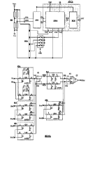
Fig.l shows a conventional transducer interface arrangement
associated to a sensor SM as generally known in the art;
Fig. 2 shows in more detail the internal circuitry of a sigma-delta
modulator SDMa forming part of an analog-to-digital converter included in a
transducer interface arrangement according to the invention;
Figs. 3 and 4 show two possible embodiments SCSa and SCSb of a
switched-capacitor module SC5 of the sigma-delta modulator SDMa of Fig. 2;
Fig.S represents the whole transducer interface arrangement
according to the invention; and
Fig. 6 shows the internal circuitry of a variant sigma-delta modulator
SDMb including gain setting possibilities in a switched-capacitor module SC1
b.
A transducer as shown at Fig. 1 is generally known in the art and
mainly includes a sensor SM adapted to measure a parameter such as pressure,
temperature, ... and an analog-to-digital converter ADC at an output OUT of
which is provided a like-named digital signal that is a function of the
measured
pa ra meter.
The sensor SM has input terminals Vexc, Vss at which an excitation
voltage is applied and output terminals CPin, CNin at which a differential
output
voltage, function of the excitation voltage and proportional to the measured
parameter, is provided. This output voltage is then applied to data input
terminals Pin, Nin of the analog-to-digital converter, or A/D converter, ADC
in
order to produce the digital output signal OUT. The measurement also comprises
the amplification of the signal at the output of the sensor SM prior to apply
it to
the input of the A/D converter ADC. To this end, the output terminals CPin,
CNin
of SM are connected to inputs of a chopper stage CHP operating as a very low
noise differential amplifier. The outputs of the chopper stage CHP are further
coupled to the data input terminals Pin, Nin of the A/D converter ADC via a
second differential amplifier VCM.
The output voltage of the sensor SM is composed out of an offset
voltage and a real differential signal of interest, and the latter is
generally much
lower than the offset voltage. In order to cover the complete range of
possible
offset and real signals, the offset voltage needs to be eliminated or at least
CA 02326019 2000-11-16
- $ _
dramatically reduced. Indeed, the offset voltage may, as an example, range
from
-17.5 mV to +17.5 mV, while the real signal is only a fraction of this and may
for instance range from 0 mV to 10 mV. In this way, if a signal with an
accuracy
of 12 bits has to be measured, the 12 bits are needed on the real input
signal,
i.e. between 0 mV and 10 mV. But since the whole range of offset and real
signals has to be covered, the A/D converter ADC should need to have an input
range from -17.5 mV (_ -17.5 mV + 0 mV) to +27.5 mV (_ +17.5 mV
+ 10 mV), and thus an accuracy of more than 14 bits. To eliminate the offset
voltage and apply only the useful differential signal as data input to the A/D
converter ADC, a selectable resistor string SRS and the differential amplifier
VCM
are added.
The selectable resistor string SRS comprises several resistors series
connected between the input terminals Vexc, Vss in order to receive the above
mentioned excitation voltage. The junction points of these resistors are
connected
to switches of which the other end is coupled to inputs of the differential
amplifier
VCM. As already mentioned, the output terminals CPin and CNin of SM are also
coupled to the inputs of the differential amplifier VCM. The switches of SRS
are
controlled by an offset correction signal OffC obtained during the calibration
cycle of the circuit. By a suitable choice of the offset correction signal
OfFC, the
inverse of the offset voltage can be applied to the inputs of the amplifier
VCM via
SRS. This inverse offset signal is then added to the composite signal coming
from
the sensor SM via the chopper CHP. Consequently, at the outputs of the
differential amplifier VCM, i.e. at the data input terminals Pin and Nin, only
the
real differential signal of interest is provided. The accuracy of the A/D
converter
ADC may so be reduced to 12 bits.
The A/D converter ADC used in a transducer application is a Sigma-
Delta modulator SDM followed by a decimation filter or decimator DCM. The
sigma-delta modulator SDM has the data input terminals Pin and Nin and an
output terminal PDM. The modulator SDM is clocked by a clock signal CLK, and
the output is a one-bit PDM signal available at the like-named output
terminal.
The digital decimation filter DCM will then convert the high frequency PDM
signal
into a low frequency 12-bit word.
CA 02326019 2000-11-16
-9-
The idea of the present invention is to combine the second amplifier
stage VCM with an input stage of the A/D converter in order to save area on
the
chip and power consumption. Furthermore, no unnecessary tolerances to the
performance of our circuit should be added. This improved solution is
described
hereafter.
The structure of a sigma-delta modulator SDMa allowing to add, in a
simple way, the extra offset cancellation is shown at Fig. 2. It is to be
noted that
in this figure a 2"d order Sigma-Delta modulator SDMa is given as an example
but that the following description is applicable on all types of Sigma-Delta
modulators.
The sigma-delta modulator SDMa has the data input terminals Pin
and Nin, reference input terminals Pref and Nref, offset input terminals Poff
and
Noff and the output terminal PDM. SDMa comprises:
- a first switched-capacitor module SC1 having differential input terminals
Pin and Nin connected to the like-named data input terminals and differential
output terminals PA1 and NA1;
- a second switched-capacitor module SC2 having differential input
terminals PSC2 and NSC2 and differential output terminals PA2 and NA2;
- a third switched-capacitor module SC3 having differential input terminals
Pref and Nref and differential output terminals PA1 and NA1;
- a fourth switched-capacitor module SC4 having differential input
terminals Pref and Nref and differential output terminals PA2 and NA2;
- a fifth switched-capacitor module SC5 having differential input terminals
Poff and Noff and differential output terminals PA1 and NA1;
- a first differential amplifier A1 having differential input terminals PAl
and
NAl and differential output terminals PSC2 and NSC2;
- a second differential amplifier A2 having differential input terminals PA2
and NA2 and differential output terminals PCP and NCP; and
- a comparator CP having differential input terminals PCP and NCP and the
single ended output terminal PDM.
All the like-named terminals are connected together.
CA 02326019 2000-11-16
-10-
The sigma-delta modulator SDMa of the invention distinguishes from
the known one SDM in that the present one includes a fifth switched-capacitor
modules SC5 controlled by an offset signal provided by the selectable resistor
string, and in that the reference signal applied to the terminals Pref and
Nref of
SC3 and SC4 is also provided by the selectable resistor string instead as
being
the excitation voltage supplied to the sensor SM.
The switched-capacitor module SC1 comprises a first set of 4
switches 1, a second set of 4 switches 2 and two capacitors C1 P and C1 N. One
end of a first capacitor C1 P is connected to a first input terminal Pin via a
first
switch 1 and to a second input terminal Nin via a first switch 2. The other
end of
C1 P is connected to a first output terminal PA1 via second switch 2 and to an
analog ground reference terminal AGND via a second switch 1. One end of a
second capacitor C1 N is connected to the first input terminal Pin via a third
switch 2 and to the second input terminal Nin via a third switch 1. The other
end
of C1 N is connected to a second output terminal NA1 via a fourth switch 2 and
to the ground reference terminal AGND via a fourth switch 1.
The switches 1 of the first set are closed during a first phase of the
clock signal CLK, whilst the switches 2 of the second set are closed during
the
second phase of this clock signal CLK, the first and second phases being non-
overlapping. This is also true for the switches 1 and 2 of the other modules
SC2
to SC5 that will be described below.
The switched-capacitor module SC2 also comprises a first set of 4
switches 1, a second set of 4 switches 2 and two capacitors C2P and C2N. One
end of a first capacitor C2P is connected to a first input terminal PSC2 via a
first
switch 1 and to the ground reference terminal AGND via a first switch 2. The
other end of C2P is connected to a first output terminal PA2 via a second
switch 2
and to the ground reference terminal AGND via a second switch 1. One end of a
second capacitor C2N is connected to the second input terminal NSC2 via a
third switch 1 and to the ground reference terminal AGND via a third switch 2.
The other end of C2N is connected to a second output terminal NA2 via a fourth
switch 2 and to the ground reference terminal AGND via a fourth switch 1.
CA 02326019 2000-11-16
The switched-capacitor modules SC3 and SC4 are similar and each
comprise a first set of .~ switches 1, a second set of 3 switches 2, a third
set of 4
switches 2- and 2+, and two capacitors: C3P and C3N for SC3, and C4P and
C4PJ for SC4. In SC3/SC4, one end of a first capacitor C3P/C4P is connected to
a first input terminal Pref via a first switch 1 and to a second input
terminal Nref
via a first switch 2. The other end of C3P/C4P is connected to a first output
terminal PA1/PA2 via a first switch 2-, to a second output terminal NA1/NA2
via
a first switch 2+, and to the ground reference terminal AGND~via a second
switch 1. One end of a second capacitor C3N/C4N is connected to the first
input
terminal Pref via a second switch 2 and to the second input terminal Nref via
a
third switch 1. The other end of C3N/C4N is connected to the first output
terminal PA1/PA2 via a second switch 2+, to the second output terminal
NA1/NA2 via a second switch 2-, and to the ground reference terminal AGND
via a fourth switch 1.
The switches 2- and 2+ of the third set are controlled by the PDM
output of the A/D converter, they are used to add or subtract the voltage at
the
reference input terminal from the differential input voltage of the
transducer.
Depending on appropriate control signals (not shown) either the switches 2- or
the switches 2+ are closed during the second phase of the clock signal CLK.
Finally, a first embodiment SCSa of the fifth switched-capacitor
module SC5 is identical to that of the first switched-capacitor module SC1
except
that the input terminals are Poff and Noff instead as Pin and Nin, and the two
capacitors C5P and C5N instead as C1 P and C1 N respectively.
In this embodiment, shown at Fig. 3, the switches of the fifth switched-
capacitor module SCSa are clocked the same way as the switches of the first
switched-capacitor module SC1. The signals at the outputs of SC1 and SC5 are
then added at the input PA1, NA1 of the first differential amplifier A1 of the
sigma-delta modulator SDMa. In other words, a conversion of the sum of the
signals at the data input terminals Pin, Nin and at the input Poff, Noff of
the fifth
switched-capacitor module is performed.
In a second embodiment SCSb of the fifth switched-capacitor module
SCS, the first mentioned end of the first capacitor C5P is connected to the
first
CA 02326019 2000-11-16
- i2 -
input terminal Poff via a first switch 2 and to the second input terminal Noff
via a
first switch 1. Furthermore, the first mentioned end of the second capacitor
C5N
is connected to the first input terminal Poff via a third switch 1 and to the
second
input terminal Noff via a third switch 2. This other embodiment is shown at
Fig. 4.
By changing the clocking of the input switches of the fifth switched-
capacitor module SC5 with respect to those of the first switched-capacitor
module
SCI, the input signal of the fifth switched-capacitor module is subtracted
from
the signal at the data input terminals. A conversion of the difference of
these
signals is then performed rather than the sum thereof.
As a result, by simply duplicating the input circuitry, i.e. the first
switched-capacitor module SC1, an extra input pair of terminals Poff, Noff is
added to the modulator at which an offset voltage may be provided for the
requested offset compensation.
Fig. 5 represents the whole transducer. Therein, the outputs of the
chopper CHP are directly connected to the data inputs Pin and Nin of the A/D
converter ADCb. The selectable resistor string SRSa is slightly modified with
respect to the one SRS shown at Fig. 1 in order to provide now both the
reference
voltage and the offset voltage.
In more detail, the selectable resistor string SRSa comprises several
resistors connected in series between the input terminals Vexc and Vss. The
junction point between a first and a second resistor in the series is
connected to
the terminal Pref, whilst the other junction points between resistors are
connected
to the terminal Poff via distinct switches controlled by an offset correction
signal
OffC. The terminal Vss is finally connected to both the terminals Nref and
Noff
off the sigma-delta modulator included in the A/D converter ADCb.
It is to be noted that although the above described sigma-delta
modulator SDMa of Fig. 2 may be included in the A/D converter ADCb of Fig. 5,
a preferred embodiment of this sigma-delta modulator, hereafter labeled SDMb
and making reference to Fig. 6, is shown. The difference between SDMa and
SDMb will be explained below.
CA 02326019 2000-11-16
- 1J -
Another improvement of the present transducer is that a gain setting is
also added inside the sigma-delta modulator thereof. This extra feature is
shown
at Fig. 6.
The sigma-delta modulator SDMb of Fig. 6 is identical to SDMa
shown at Fig. 2 except for the first switched-capacitor module SC1 b that now
includes gain setting modules. These gain setting modules are constituted by
one
or more branches coupled in parallel across the first Cl P and the second C1 N
capacitors of SC1. The branches each comprises the series connection of an
extra capacitor C1' and an extra switch SG. These extra switches SG,
controlled
by a digital gain control signal applied to a gain setting input GS of SDMb,
as
shown at Fig. 5, are not clocked but are switched on or off depending on the
desired gain. By adding the extra capacitors in parallel with the existing
capacitors C1 P and C1 N, the gain or input range of the modulator can be
changed. The more capacitors we add, the higher the gain.
While the principles of the invention have been described above in
connection with specific apparatus, it is to be clearly understood that this
description is made only by way of example and not as a limitation on the
scope
of the invention, as defined in the appended claims.