Note: Descriptions are shown in the official language in which they were submitted.
CA 02326044 2006-05-15
23940-1191
1
SWITCHING CIRCUIT WITH INTERMITTENTLY LOADED CHARGED
CAPACITANCE
The present invention relates a switching circuit.
In particular, the present invention relates to a switching
circuit comprising a switch which on activation discharges a
capacitance.
Typically, a switching circuit utilises a switch
to complete an electrical circuit. When the switch is
closed the circuit is closed and when the switch is open the
circuit is open. One disadvantage of such a switch is that
power is dissipated while the switch remains closed.
It would be desirable to provide a switching
circuit which consumes less power.
According to one aspect of the present invention,
there is provided a switching circuit, comprising: a first
node for receiving a first voltage; a second node for
providing an output; a third node for receiving a second
voltage; a capacitance coupled between the second node and
the third node; an intermittent charger that intermittently
charges the capacitance to provide a first output voltage
from the second node; a first switch connected between the
first node and the second node for isolating the second node
from the first node when open and for discharging the
capacitance to provide a second output voltage when closed;
and a buffer connected to said second node, said buffer
being electrically conductively connected to said first
switch when said first switch is closed, said buffer
providing an output indicating when said first switch is in
a closed position.
CA 02326044 2006-05-15
.23940-1191
1a
The present invention also provides a switching
circuit, comprising: a first node for receiving a first
voltage; a second node for providing an output: a third node
for receiving a second voltage; a capacitance coupled
between the second node and the third node; means for
intermittently charging the capacitance to provide a first
output voltage from the second node; and a switch connected
between the first node and the second node for isolating the
second node from the first node when open and for
discharging the capacitance to provide a second output
voltage when closed.
In one embodiment the switching circuit further
comprises a buffer connected to the second node.
In another embodiment the switching circuit
further comprises a latch connected to the second node.
Preferably, the latch is a Schmitt trigger latch.
Preferably, the means for charging the capacitance
comprises a second switch responsive to a control signal for
connecting the second node to a voltage source.
CA 02326044 2000-09-26
WO 99/50961 PCT/SE99/00538
2
In a preferred embodiment the control signal is a pulsed signal.
Preferably, the duration of a pulse is substantially less than the period
between pulses.
s More preferably, the pulse has a duration which is 1/500 of its period.
Preferably, the pulse has a duration of about 1 ms.
Preferably, the voltage source is a positive voltage and the first and second
voltages are
i o ground.
In one embodiment the capacitance comprises a stray capacitance.
Preferably, the switching circuit comprises a capacitor for providing at least
a portion of
~s the capacitance.
It will be appreciated that in the present invention, when the first switch is
open, power is
dissipated only while the capacitance charges. Once the capacitance has been
charged and
when the first switch is open negligible current will be drawn by the
capacitor and
2o negligible power will be consumed. When the first switch is closed, the
voltage at the
second node quickly discharges. When the second switch is then closed, the
voltage at the
second node increases in a stepwise fashion as the capacitance is
intermittently charged.
The voltage at the second node will depend upon the total charge supplied by
the means for
intermittently charging the capacitance and the value of the capacitance.
2s
A preferred embodiment of the present invention will now be described
hereinbelow by
way of example only with reference to the accompanying drawings, in which:
Figure 1 is a schematic diagram of a switching circuit in accordance with a
preferred
3o embodiment of the present invention;
CA 02326044 2000-09-26
WO 99/50961 PCT/SE99/00538
3
Figure 2 is a schematic diagram of debounce circuitry in the switching circuit
of Figure 1;
Figure 3 is a schematic diagram of a clock generator for use with the
switching circuit of
Figure 1;
Figure 4 illustrates a pulsed signal output from the clock generator of Figure
3; and
Figure 5 illustrates the signal input to the clock generator of Figure 3.
io
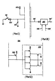
The switching circuit 500 includes a switch 501 which includes first and
second terminals
and a mechanism having a first configuration in which the first terminal is
connected to the
second terminal and a second configuration in which the first and second
terminals are
mutually electrically isolated. The first terminal of the switch 501 is
connected to ground
~s and the second terminal of the switch SO1 is connected to an input node
502. A
capacitance 506 exists between the input node 502 and ground. This capacitance
may be a
stray capacitance between the input node 502 and ground or a capacitor
connected between
the input node 502 and ground. The switching circuit 500 includes a p-channel
FET 508,
with a source connected to a positive voltage Vpn and a drain connected to the
input node
zo 502. The switching circuit 500 further includes a Schmitt trigger 510. The
input node 502
is connected to the input of a Schmitt trigger 510 and the output of the
Schmitt trigger 510
produces an output signal 105. The output signal 105 is then supplied to
debounce
circuitry 602 which is controlled by a reset signal 1301 and an Fdebounce
signal 403. The
gate of the p-channel FET 508 receives a pulsed signal 603 from a clock signal
generator
2s 400. The form of the pulsed signal 603 is illustrated in Figure 4.
Generally, the pulsed
signal 603 is high and is pulsed low at regular intervals with a frequency of
1 kHz. The
duration of the pulse is from 1.5 to 3 ps which equates to a duty cycle of
approximately
1/500. When the pulsed signal 603 is high the p-channel transistor 508 is
switched off.
When the pulsed signal 603 is pulsed low the transistor 508 switches on
momentarily and
3o charges the capacitor 506. When the first switch 501 is closed the input
node 502 is
CA 02326044 2000-09-26
WO 99150961 PCT/SE99/00538
4
connected to ground and the capacitor 506 is quickly discharged. The
discharging of the
capacitor 506 causes the output state of the Schmitt trigger 510 to change
state causing the
output signal 105 to be asserted high. When the first switch SO1 is opened,
the capacitor
506 is charged via the transistor 508 and the voltage at the input node 502
rises. The rising
voltage, when passing a threshold value, causes the output state of the
Schmitt trigger 510
to return to a low value. The voltage at the input node 502 is dependent on
the current
supplied by the transistor 508 and the value of the capacitance 506. By
selecting the
capacitance 506 and/or the size of the transistor 508 the latency between the
opening of the
switch 501 and the change in the output signal 105 can be controlled. The use
of a pulsed
~o signal to operate the p-channel transistor 508 reduces power consumption.
The debounce circuitry is illustrated in further detail in Figure 2. The
debounce circuitry
receives the signal to be debounced 105, the reset signal 1301 and the
Fdebounce signal
403 which is a regular square wave clock signal with a frequency of about 1
kHz. The
~s signal to be debounced 105 is supplied to the input of a first D flip-flop
606. The non-
inverted output of the first flip-flop 606 is supplied as an input to a second
D flip-flop 608
and as a first input to a first three-input NAND gate 612. The inverted output
of the first
flip-flop 606 is supplied to a first input of a second three-input NAND gate
614. The non-
inverted output of the second flip-flop 608 is supplied as an input to a third
D flip-flop 61.0
2o and as a second input to the first three-input NAND gate 612. The inverted
output of the
second flip-flop 608 is supplied to a second input of the second three-input
NAND gate
614. The non-inverted output of the third flip-flop 6I0 is supplied as a third
input to the
first three-input NAND gate 612. The inverted output of the third flip-flop
610 is supplied
to a third input of the second three-input NAND gate 614. The outputs of the
first and
is second NAND gates 612, 614 are supplied as inputs to an SR flip-flop 616,
the output of
which is the debounced signal. Each of the flip-flops is reset by the reset
signal 1301 if
asserted. Each of the D flip-flops is clocked by the Fdebounce signal 403.
Consequently,
if the input signal 105 has a transition from low to high, for example, and
remains high for
three clock cycles of the Fdebounce signal 403, then the debounced signal 105'
also has a
CA 02326044 2006-05-15
23940-1191
transition from low to high. If the input signal goes low,
the debounced signal 105' goes or remains low.
Referring to Figure 3, an output signal from an
oscillator is supplied as an input signal 201 to a clock
5 generator 400. In some embodiments, the oscillator output
signal illustrated in Figure 5 may be the input signal 201
to the clock generator 400. The clock generator 400
produces pulsed signal 603 and Fdebounce signal 403. The
input signal 201 is illustrated in Figure 3. The pulsed
signal 603 and the Fdebounce signal 403 have a frequency of
about 1 kHz. However, the pulsed signal 603 is generally
high but pulsed low for a few microseconds in each period
whereas the Fdebounce signal 403 is a regular symmetric
signal being high half of the time and low half of the time.
Referring to Figure 3, the clock generator 400 has
an inverter 410 for inverting the input signal 201 to
produce an inverted signal 411. The inverted signal 411 is
then supplied to the first one of a linear series of five
frequency dividers 420. The output of each frequency
divider 420 toggles on a rising edge at its input. Each
frequency divider receives a clock signal and produces a
regular square wave clock signal, with half the frequency of
the input signal as an input to the next frequency divider
in the linear series. The Fdebounce signal 403 is taken
from the output of the fifth frequency divider. The
inverted signal 411, the output of the first frequency
divider 420a and the output of the second frequency divider
420b are combined in a NOR gate 430a to produce a signal
413. The output from the third, fourth and fifth frequency
dividers 420c, 420d, and 420e are each supplied to an input
of a NOR gate 430b which produces a signal 415. The signals
413 and 415 are input to a NAND gate 432 to produce the
pulsed signal 603.
CA 02326044 2006-05-15
X3940-1191
6
Finally, it will be understood that the present
invention has been described in its preferred embodiment and
can be modified in many different ways within the scope of
the appended claims.