Note: Descriptions are shown in the official language in which they were submitted.
CA 02326082 2000-11-14
NL2906-C2501-dV/jdh
Connector
The invention relates to a connector, comprising a
- housing of insulating material, the housing having a mounting
surface with means for mounting the housing on the surface of a
printed circuit board.
EP-A-0 930 812 discloses a connector of this type,
wherein the mounting means is provided in the form of a metal
plate mounted on the mounting surface. The mounting surface is
provided with pegs, wherein the metal plate is fixed by melting
the pegs. The known manner of fixation of the metal plate to
the housing is disadvantageous as heating the pegs causes de-
generation of the insulation material resulting in an unreli-
able fixation of the metal plate and/or problems regarding lo-
cation or fixation of the contact elements accommodated in the
housing. Moreover the fixation step in manufacturing the con-
nector is relatively time consuming and involves relatively
high production cost.
The invention aims to provide an improved connector of
the above-mentioned type.
To this end the connector of the invention is charac-
terized in that the mounting surface is provided with a plural-
ity of grooves, each groove having a groove entrance directed
away from the mounting surface, wherein a metal connection ele-
ment is mounted in each groove by clamping, which connection
element is accessible through the groove entrance.
In this manner a connector is obtained, wherein the
connection elements providing the surface mount connection to
the printed circuit board are mounted in the nrooves hl~ a sim-
ple clamping connection. Manufacturing cost of the connector
are thereby reduced, whereas a reliable connection is neverthe-
less guaranteed.
In a first embodiment the metal connection elements
are made as solid rods.
Preferably, the metal connection elements are made as
CA 02326082 2000-11-14
2
hollow tubes with at least one opening accessible through the
groove entrance and connecting t;he hollow inner side of the
tube with the environment. In particular this embodiment allows
... a very strong interconnection between the connection elements
_ 5 and the housing as the tubes can be relatively resilient,
whereas after the soldering step for connecting the connector
-~ to the printed circuit board, the hollow tubes will be filled
with soldering material resulting in solid tubes which can not
be removed from the grooves.
The invention will be further explained by reference
to the drawings in which two embodiments of the connector of
the invention are schematically shown.
Fig. 1 is perspective view of an embodiment of the
connector of the invention showing the mounting surface of the
connector.
Figs. 2- 4 show details of the connector of fig. 1.
Fig. 5 shows the connector of fig. 1 mounted on a
printed circuit board with two details at a larger scale show-
ing the solder interconnection between the connection elements
and the printed circuit board.
Fig. 6 shows a perspective view of a second embodiment
of the connector of the invention, wherein the connection ele-
ments are shown before assembly with the connector.
Fig. 7 shows a perspective view corresponding to fig.
6 with the connection elements mounted in the grooves of the
mounting surface.
Figs. 8A-8C show the mounting step of a connection
element in the embodiment of fig. 6.
Fig. 9 shows the connector of fig. 7 as mounted on a
printed circuit board with two details at a larger scale.
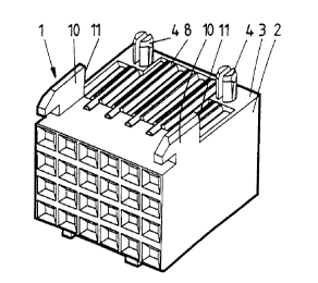
Fig. 1 shows a perspective view of a connector 1 com-
prising a housing 2 ~f_ insulating material. The housing 2 has a
mounting surface 3 having two projecting spring-type pegs 4 for
holding the connector 1 on the surface of a printed circuit
board before making a solder connection.
The mounting surface 3 of the housing 2 is provided
with a plurality of grooves 5 having upstanding side walls 6 as
can be seen in figs. 2 and 3 in particular. The outer ends of
_.i
CA 02326082 2000-11-14
3
the upstanding side walls 6 det=ermine a groove entrance 7 di-
rected away from the mounting surface 3. A connection element 8
is mounted in each groove 5 by pressing the connection element
through the groove entrance 7 into the groove. The upstanding
side walls 6 will resiliently deform so that the connection
element 8 will be received in the groove 5 as shown in fig. 3.
In case of the connector shown in fig. 1, the connec-
tion elements 8 are made as solid metal rods. The solid metal
rods are pre-tinned, i.e. provided with a tin coating before
mounting the rods into the grooves 5. The rods 8 are clamped
within the grooves 5 as the diameter of the rods 8 fits clamp-
ingly within the groove 5, wherein the width of a groove en-
trance 7 is smaller than the diameter of the rod 8. As can be
seen in fig. 1-4, the rods 8 extend into groove extensions 9
which are made in a part of the mounting surface 3 between two
upstanding elements 10 determining a stop 11 co-operating with
an edge 12 of a printed circuit board 13 shown in fig. 5.
Fig. 5 shows the connector 1 of fig. l as mounted on
the printed circuit board 13, wherein the pegs 4 are received
in corresponding passages 14 of the printed circuit board 13.
On the surface of the printed circuit board 13 directed towards
the mounting surface 3 circuit tracks 15 are provided adapted
to co-operate with the rods 8 mounted in the grooves 5. These
circuit tracks 15 are provided with a solder paste in a usual
manner. For making the solder connection, the solder paste is
heated and as the rods 8 extend beyond the edge 12 of the
printed circuit board 13, the heat received by the ends of the
rods 8 allow a rapid absorption of heat energy and subsequent
transmission of the heat along the complete length of the rods
8. In this manner a reliable interconnection between the rods 8
and the circuit tracks 15 is obtained a shown in ttie details at
a larger scale of fig. 5.
Figs. 6-9 show a second embodiment of the connector of
the invention which mainly corresponds to the embodiment of
figs. 1-5, wherein corresponding elements are indicated by the
same reference numerals. The connector 20 shown in figs. 6-9
comprises the same housing 2 as the connector 1 of figs. 1-5.
In this case the connection elements are made as hollow tubes
CA 02326082 2000-11-14
.,W
... 4
21 having at least one opening 22 which is accessible through
the groove entrance 7 when the hollow tubes 21 are mounted in
the grooves 5. The opening 22. of the tubes 21 connect the hol-
low inner side of the tube with the environment. This opening
_ 5 22 is made as a longitudinal slot in the embodiment shown in
' figs. 6-9. As shown in particular in figs. 8A-8C the longitude-
nal slot 22 provides the tube 21 with a cross-section which can
be decreased by resilient deformation during mounting the tube
21 in a groove 5. In fig. 8B the tube 21 is compressed by the
upstanding side walls 6 such that the longitudinal slot 22 is
substantially closed. When the tube 21 is completely received
within the groove 5, the tube 21 flexes outwardly again to open
the slot 22. In this manner the situation of fig. 7 is obtained
showing the connector 20 before mounting the same on the
printed circuit board 13. Fig. 9 shows in the same manner as
fig. 5 the connector 20 as mounted on the printed circuit board
13. Again, the edge 12 of the printed circuit board 13 engages
the stops of the elements 10 so that the hollow tubes 21 extend
beyond the printed circuit board 13 and thereby allow a rapid
absorption of energy to provide a re-flow of the solder paste
on the circuit tracks 15. The tubes 21 are tinned both on the
outer and inner sides. Through re-flowing the solder paste, the
soldering material will flow into the hollow inner side of the
tubes 21 as indicated by reference numeral 23 resulting in a
solid connection element after the soldering step. In this man-
ner a very rigid anchorage of the connection elements in the
grooves 5 of the housing 2 is obtained.
The hollow tubes 21 can be made from a flat metal
strip by stamping an deforming in a manner known per se. In
fig. 6 the tubes 21 are still interconnected to a strip 24,
wherein they are separated from the strip 24 when they are as-
sembled with the housing. In the embodiments shown the connec-
tion elements have different lengths. Of course, all connection
elements may have the same length. In the embodiment of fig. 1-
5 the connection elements can be cut off from tinned wires.
The invention is not restricted to the above described
embodiments which can be varied in a number of ways within the
scope of the claims.