Note: Descriptions are shown in the official language in which they were submitted.
CA 02326244 2000-11-16
-1-
ELECTRICAL CONNECTING ELEMENT AND
METHOD OF PRODUCING THE SAME
background of the Invention
This invention relates to electrical connecting elements such as
connectors for electrically connecting wiring or circuit boards with each
other,
and anisotropic conductive elements for interconnecting terminals, electrodes,
etc. on flexible printed wiring or circuit boards such as flat cables and
circuit
boards, and a method of producing the same.
Heretofore, the prior art connectors for electrically connecting wiring
to boards with each other, for example have generally required
mechanisms/members for mechanically fixing the connectors and the wiring
boards and maintaining the boards connected as well as members for
establishing the connection. Conventional connectors having such
mechanical coupling means have been correspondingly complicated in
15 structure, resulting in hampering the miniaturization and slimming-down.
Japanese Patent Publication No. 7-220846 issued August 18, 1995 discloses
producing a connector by bonding a metallic thin sheet to an insulating
cushioning material and laser-machining channels in the metallic thin sheet,
followed by bending the assembly perpendicularly to the channel machining
2o direction into a U-shape with the cushioning material facing inward. This
required machining channels by laser on connectors one by one, rendering the
manufacturing process cumbersome.
On the other hand, to take the conventional manufacturing of flexible
printed wiring boards (FPC) by example, the process involves forming a
2s required conductor pattern on a substrate (base film), followed by laying a
covering over the conductor pattern to protect and insulate the latter.
However, it required a dedicated adhesive to bond the covering to the
CA 02326244 2000-11-16
-2-
substrate, and involved an additional step to apply the adhesive.
Accordingly, it is an object of this invention to provide an electrical
connecting element which is easy to manufacture, and a method of producing
the same.
Another of this invention is to provide an electrical connecting element
which is of simple construction and allows for reduction in size and
thickness,
and a method of producing the same.
According to one aspect of this invention, a metallic thin film is formed
to on a mold having protrusions complementary in shape to a conductor pattern
to be formed, and a transfer layer of adherent (or sticky) material or
adhesive
material is applied to the metallic thin film laid over the protrusions,
followed
by pulling the transfer layer apart from the mold so as to transfer the
metallic
thin film covering the protrusions onto the transfer layer to thereby form the
is conductor pattern on the transfer layer.
Alternatively, the transfer layer may be applied to one side surface of the
substrate. The term "adherent material" used herein refers to the material
with which two objects will be bonded together in such a manner that they
may be subsequently peeled apart at the joined surfaces while the term
20 "adhesive material" used herein refers to the material with which two
objects
will be bonded together in such a manner that they may be hardly peeled apart
at the joined surfaces.
In an alternative embodiment, the metallic thin film may be of multi-
layer construction including a prime layer having a weak adhesion to the
2s mold.
The electrical connecting element according to this invention comprises
a substrate having a transfer layer of adherent material or adhesive material
CA 02326244 2000-11-16
-3-
thereon, and a conductor pattern provided on the transfer layer. The
conductor pattern is obtained by forming a metallic thin film on a mold
having protrusions corresponding to the conductor pattern, adhering the
substrate to the metallic thin film laid over the protrusions by means of the
transfer layer, followed by pulling the substrate away from the mold so as to
have the metallic thin film laid over the protrusions transferred onto the
transfer layer to thereby form the conductor pattern thereon.
The connector for use as an electrical connecting element according to
this invention for electrically connecting wiring boards with each other
to comprises a wiring element composed of a substrate having a transfer layer
of
adherent material or adhesive material applied to one side surface thereof,
and
a conductor pattern having a plurality of parallel conductor lines formed on
the transfer layer. The conductor pattern is obtained by forming a metallic
thin film on a mold having ridge-like protrusions corresponding to the array
15 of the conductor lines, adhering the transfer layer side of the substrate
to the
metallic thin film laid over the protrusions, followed by pulling the
substrate
away from the mold so as to have the metallic thin film on the protrusions
transferred onto the transfer layer to thereby form the conductor pattern
thereon, wherein the conductor lines of the conductor pattern is in opposing
2o contact with the respective wiring lines to be connected of the two wiring
boards being connected to thereby establish connection between those wiring
lines, the substrate being pressed against the two wiring boards such that
those portions of the transfer layer between the adjacent conductor lines are
adherently (or stickily) attached to the surfaces of the two wiring boards to
25 form a mechanical bond.
In an alternative embodiment, the wiring element may be folded in two
along a fold line extending in the direction of arrayal (transversely) of the
CA 02326244 2000-11-16
-4-
conductor lines of the conductor pattern with the conductor pattern side
facing
outwardly to form a connector for use as an electrical connecting element.
Preferably in this case, the wiring element is folded back by 180
° and a
spacer or retainer member is sandwiched between the folded legs of the
element so that the wiring element may be secured to the retainer member.
In an alternative embodiment, the connector for use as an electrical
connecting element comprises two of the wiring element constructed
according to this invention. The two wiring elements are bonded together
with the conductor patterns of one halves of the respective wiring elements in
opposing contact with each other by virtue of the transfer layers of the two
wiring elements being adherently attached together while the substrates of the
other halves of the respective elements have spacers affixed thereto on the
side opposite from the side on which the respective conductor patterns are
formed.
m The flexible printed wiring board for use as an electrical connecting
. element according to this invention comprises a covering laid over the
surface
of the wiring element according to this invention on which the conductor
pattern is formed, the covering being bonded to the element by means of the
transfer layer.
2o The anisotropic conductive element for use as an electrical connecting
element according to this invention comprises the wiring element according to
this invention having a conductor pattern composed of a number of conductor
lines arranged parallel to each other at a predetermined pitch, the thus
constructed wiring element being cut orthogonally to the length of the
25 conductor lines into strips, a plurality of which are in turn stacked one
on
another in vertical alignment with each other, the thus built-up strips being
pressed together in the direction of stacking to be laminated together in one
CA 02326244 2004-03-08
- 5 -
piece assembly.
A method of producing an anisotropic conductive element for use
as an electrical connecting element according to this invention comprises
the steps of providing a mold having a multiplicity of grooves formed in
s the surface thereof in a grid pattern and a multiplicity of protrusions, one
extending from the top of each of the rectangular raised sections
surrounded by the grooves; forming a metallic thin film on the mold
having the protrusions; providing a transfer layer of adherent material or
adhesive material having a release sheet applied on one side thereof and
~ o penetrating the protrusions of the mold into and through the transfer
layer
into abutment against the release sheet to thereby bring those portions of
the metallic thin film covering the side surfaces of the protrusions and the
surfaces of the rectangular raised sections into close contact with the
adherent material or adhesive material; pulling the transfer layer together
1 s with the release sheet apart from the mold; then removing the release
sheet from the transfer layer to complete an anisotropic conductive
element having formed thereon a multiplicity of conductor patterns
penetrated through and held by adherent material or adhesive material.
In accordance with one aspect of the present invention there is
ao provided a method for producing an electrical connecting element,
comprising the steps of: (a) forming a metallic thin film on a mold
having a plurality of raised ridges in an array corresponding to a
conductor pattern of a plurality of conductor lines spaced from one
another to be formed; (b) adherently attaching a transfer layer comprising
2s an adherent material or an adhesive material formed on a substrate to said
metallic thin film laid over the plurality of raised ridges, said transfer
layer being more easily deformable than said substrate; and (c) separating
CA 02326244 2004-03-08
-Sa-
said substrate together with said transfer layer having the metallic thin
film adherently attached thereto from said mold so as to transfer said
metallic thin film covering tops of said raised ridges onto the transfer
layer to thereby form an electrical connecting element having said
s conductor pattern of said plurality of conductor lines formed on the
transfer layer on said substrate with surface areas of said transfer layer
between said conductor lines being exposed to be adhered to an object to
be attached thereto.
In accordance with another aspect of the present invention there is
to provided an electrical connecting element comprising: a substrate; a
transfer layer made of either one of adherent material and adhesive
material formed on said substrate, said transfer layer being more easily
deformable than said substrate; and a conductor patter of an array of
conductor lines spaced from one another and adherently attached to said
~ s transfer layer by means of adherent power of the transfer layer itself,
surface areas of said transfer layer between said conductor lines being
exposed to be adhered to an object.
Brief Description of the Drawings
Zo Fig. 1 is a schematic diagram illustrating the sequential steps of
one embodiment of the method of producing the electrical cormecting
element according to this invention;
Fig. 2 is a perspective view of the mold 11 shown in Fig. l;
Fig. 3 is a perspective view of an embodiment of the wiring
Zs element for use as an electrical connecting element according to this
invention manufactured by the process illustrated in Fig. 1;
Fig. 4A is a perspective view illustrating an embodiment of the
CA 02326244 2000-11-16
-6-
connector for use as an electrical connecting element according to this
invention;
Figs. 4B and 4C are perspective views illustrating how wiring boards are
connected with each other by the connector shown in Fig. 4A;
Fig. SA is a perspective view illustrating another embodiment of the
connector for use as an electrical connecting element according to this
invention;
Fig. SB is a side view illustrating the wiring boards connected with each
other by the connector shown in Fig. SA;
Fig. 6A is a perspective view illustrating yet another embodiment of the
connector for use as an electrical connecting element according to this
invention;
Fig. 6B and 6C are perspective views illustrating how wiring boards are
connected with each other by the connector shown in Fig. 6A;
15 Fig. 7 is a perspective view illustrating an embodiment of the flexible
printed wiring board for use as an electrical connecting element according to
this invention;
Fig. 8A is a perspective view illustrating another embodiment of the
connector stock manufactured by the method according to this invention;
2o Fig. 8B is a perspective view illustrating strips cut from the stock shown
in Fig. 8A being stacked one on another;
Fig. 8C is a perspective view illustrating an embodiment of the
anisotropic conductive element for use as an electrical connecting element
according to this invention;
2s Fig. 9 is a schematic diagram illustrating the sequential steps of another
embodiment of the method of producing the electrical connecting element
according to this invention;
CA 02326244 2000-11-16
Fig. 10 is a perspective view showing a part of the mold 11 shown in Fig.
9; and
Fig. 11 is a perspective view illustrating another embodiment of the
anisotropic conductive element for use as an electrical connecting element
according to this invention.
Detailed Description of the Preferred Embodiment
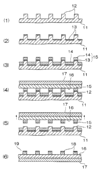
Fig. 1 illustrates the sequential steps of one embodiment of the method
of producing the electrical connecting element according to this invention.
The steps will be described specifically below.
to (1) A mold 11 is provided. The mold 11 has formed in its surface
protrusions 12 corresponding to a conductor pattern to be formed. In the
example illustrated, the protrusions 12 comprise a plurality of raised ridges
arrayed at a predetermined pitch, as shown in Fig. 2, although the raised
ridges need not necessarily be arrayed at equal intervals.
(2) First, on the mold 11 a metallic film having a relatively weak
adhesion (weak adherent power) to the mold is formed by vapor deposition,
sputtering deposition or plating (either electroless plating or electrolytic
plating) to provide a prime layer I3.
(3) The next step is to form on this prime layer 13 a main conductor
2o Iayer 14 in the form of a film to a predetermined thickness from which a
conductor pattern are to be formed. This film forming is effected by vapor
deposition, sputtering deposition or plating (electroless plating and/or
electrolytic plating) to thereby provide a two-ply metallic thin film 15
composed of the prime layer 13 and the main conductor layer 14.
2s (4) Next, a substrate 17 having a transfer layer 16 of adherent material
applied to one side surface thereof is provided. The substrate 17 is oriented
with its transfer layer 16 facing toward the mold 11 and the transfer Iayer 16
CA 02326244 2000-11-16
_$_
is then brought into intimate contact with the metallic thin film 15 on the
protrusions 12.
(5) The transfer layer 16 together with the substrate 17 is pulled up
away from the mold 11. In doing so, the metallic thin film 1 S on the
protrusions 12 which is now adherently attached to the transfer layer 16 is
peeled apart from the mold 11 at the interface with the mold.
(6) That is, the metallic thin film 15 on the protrusions 12 is transferred
and adherently attached onto the transfer layer 16. It is thus to be
appreciated that a wiring element 19 is completed which comprises the
Io substrate 17 and a conductor pattern 18 formed of the metallic thin film 15
transferred onto the transfer layer 16. Fig. 3 shows the entire configuration
of the thus completed wiring element 19.
In the method of forming a conductor pattern as described above, gold,
tin or carbon which is poorer in adherence to the mold 11 than the main
conductor layer 14 may be used for the material of which the prime layer 13
is formed while nickel or copper may be used for the material of which the
main conductor layer 14 is formed. Forming the main conductor layer 14 of
nickel or copper will provide the 'conductor pattern 18 which have a desired
mechanical strength and which may be provided with conductivity as required.
2o The prime layer 13 need only allow the metallic thin film 15 to be peeled
apart from the mold 11 at the interface, and may be very thin even on the
order of 0.005 ,u m. However, if the prime layer 13 is made of gold to
enhance the conductivity of the conductor pattern 18, it may be on the order
of say 0.05 ,u m. It is desirable from the viewpoint of mechanical strength
that the main conductor layer 14 be more than 3 ,u m in thickness.
Various materials such as glass, silicon, stainless steel and fluoroplastics
may be used for forming the mold 11. When the mold 11 is made of
CA 02326244 2000-11-16
-9-
fluoroplastics, which is extremely poor in adhesion to metallic film, a main
conductor layer 14 of nickel or copper may be formed directly on the mold 11
without the need for intervening the prime layer 13 as of gold or tin, and the
main conductor layer 14 as such may be easily removed from the mold 11 at
the interface. The need for the prime layer 13 may also be eliminated by
fluoridizing the surface of the mold 11 made of glass, silicon or stainless,
or
by oxidizing the surface of the mold 11 in the case that the latter is made of
silicon.
Concerning the formation of the protrusions 12 on the mold 11. such
to protrusions 12, if they are in the form of raised ridges as in the example
illustrated, may be easily formed in an array at a predetermined pitch by
channelling in the surface by the use of a dicing saw, for example.
Depending on the configuration and dimensions of the protrusions 12, the
etching process may also be utilized. By way of example, when a conductor
15 pattern 18 to be formed is composed of conductor lines of miniscule size
and
arrayed at a fine pitch, it is possible to adopt such a method as making a
mold
11 of silicon and forming protrusions 12 by dry etching utilizing a mask.
With the use of a dicing saw, it is possible to make the pitch of protrusions
12
as fine as 100um while the use of dry etching allows for making the pitch of
2o protrusions 12 as fine as 1 Vim. It is to be noted that the depth of the
channels
should be greater than the thickness required of the metallic thin film 15.
For the substrate 17, either a flexible substrate such as polyimide resin or
the like or a rigid substrate such as glass, epoxy resin or the like may be
selectively used depending on the application of the wiring element 19.
2s While the transfer layer 16 of adherent material maintaining stickiness is
disposed on one side surface of the substrate 17 in the example illustrated,
the
adherent material may be replaced by a transfer layer 16 of adhesive material
CA 02326244 2000-11-16
- to -
which will cure after a lapse of a predetermined period of time.
Further, depending on the application, the main conductor layer 14 may
be made of gold, in which case the metallic thin film 15 will be formed of a
single layer of gold. In addition, in order to ensure symmetry as vertically
aligned conductor patterns 18 and to prevent oxidization of the main
conductor layer 14 made of nickel or copper, the same metallic film as the
prime layer 13 may be additionally formed on the main conductor layer 14, in
which case the metallic thin film 15 will be of a three-ply construction of
gold/nickel/gold.
~o Fig. 4 illustrates how a wiring element manufactured by using the
conductor pattern forming process as described above (which will be referred
to as "transfer method" hereinafter) is used for a connector as an electrical
connecting element. As shown in Fig. 4A, the connector 21 includes a
conductor pattern 18 comprising a plurality of conductor lines arranged
15 parallel to each other at a predetermined pitch on a transfer layer 16 of
adherent material applied to one side surface of a substrate 17.
The connector 21 is used to connect two wiring boards 22 with each
other as shown in Fig. 4B. The wiring boards 22 are lined end to end such
that the wirings 23 at the ends to be connected are in line with each other
and
2o the connector 21 is brought into pressure contact with the two wiring
boards
22 with the conductor patterns 18 of the connector 21 positioned in opposition
to the corresponding wirings 23 to be connected as shown in Fig. 4C. This
pressure contact brings the wirings 23 of these two wiring boards 22 into
electrical connection with each other as well as forcing the conductor pattern
25 18 of the connector 21 into the transfer layer 16 whereby those portions of
the
transfer layer 16 between the conductor pattern 18 are adherently attached to
the corresponding surface portions of the two wiring boards 22 to provide
CA 02326244 2000-11-16
-11-
mechanical bonding between the connector 21 shown in and the two wiring
boards 22. The degree of the bonding by means of the transfer layer 16 may
be determined by selecting the thickness of the transfer layer 16 in
consideration of the thicknesses of the conductor pattern 18 and the wirings
23.
The transfer layer 16 is subjected to elastic deformation by the conductor
pattern 18 forced thereinto to thereby be adherently attached to surface
portions of the two wiring boards 22, so that the elastic restoring force of
the
transfer layer contributes as a load acting in the sense to urge the conductor
to pattern 18 into contact with the wirings 23 whereby good electrical
connection may be established between the conductor pattern 18 and the
wirings 23.
The construction of this connector 21 eliminates the need for a separate
dedicated member (part) for mechanically securing the connector to the two
m wiring boards 22 by utilizing the transfer layer 16 not only for forming the
conductor pattern 18 through the transfer by virtue of stickiness, but also
for
providing mechanical securement to the wiring boards 22 to be interconnected.
It is thus to be appreciated that the connector 21 according to this invention
is
simple in construction and may be formed in a very low profile. In addition,
2o it should be understood that the transfer layer 16 may be repeatedly
(detachably) used by choosing an appropriate adherent material of which the
transfer layer is formed or alternatively that permanent connection may be
provided, if desired, by using an adhesive material to form the transfer layer
16.
25 Fig. 5 illustrates another embodiment of the connector for use as an
electrical connecting element according to this invention in which a wiring
element 19 having a conductor pattern 18 comprising a plurality of conductor
CA 02326244 2000-11-16
-12-
lines formed in an array by the transfer method as described above is folded
by 180 ° along a fold line extending in the direction of arrayal of the
conductor lines with the conductor pattern 18 side facing outwardly and a
spacer or retainer member 24 in the form of a thin plate is sandwiched
s between the folded legs of the element to form a connector 25, as shown in
Fig. SA. The radius of curvature of the fold may be on the order of 0.2 mm,
for example.
In the example illustrated, the substrate 17 is in the form of film of
polyimide resin, for example or the like which may be easily folded, and has a
to transfer layer 16 applied on one side surface thereof on which conductor
lines
are formed in an array to constitute a conductor pattern 18.
The wiring element 19 is maintained in its folded position by the retainer
member 24 to which the inner opposed of the folded wiring element 19 are
fixed by an adhesive, for example.
The retainer member 24 in the form of a thin plate is made of glass sheet
or a sheet of epoxy resin or the like, although it may be formed of an elastic
material such as rubber.
This connector 25 is designed to be sandwiched in use between two
wiring boards 22 to be interconnected as shown in Fig. 5B so as to connect
2o the two wiring boards 22 having their wiring faces opposed to each other.
It is thus to be understood that this connector connection is established
by sandwiching and compressing the connector 25 between two wiring boards
22 to be connected with the conductor pattern I8 facing in opposition to the
wirings 23 of the two wiring boards 22 whereby the mechanical connection as
25 well as electrical connection is effected in the same manner as with the
connector 21 illustrated in Fig. 4.
Fig. 6 illustrates another embodiment of the connector for use as an
CA 02326244 2004-03-08
-13-
electrical connecting element for connecting two wiring boards having their
wiring faces facing inwardly (but not necessarily facing in opposing
relation).
In this example, as shown in Fig. 6A, a pair of wiring elements 19 each
having a conductor pattern 18 comprising a plurality of conductor lines
s formed in an array by the transfer method as described above are positioned
with the conductor patterns of one halves, as viewed lengthwise of the
conductor lines, of the respective elements 19 in opposing contact with each
other and bonded together by virtue of the transfer layers of the two wiring
elements being adherently attached together as a result of being pressed such
that those portions of the outer substrates 17 backing the transfer layers of
the
one halves are urged toward each other while the substrates 17 of the other
halves of the respective wiring elements 19 have spacers 26 affixed thereto on
the side opposite from the side on which the conductor patterns 18 are
formed.
is Like the connector 25 shown in Fig. 5, the connector 27 is sandwiched in
use between two wiring boards 22.as shown in Fig. 6B wherein the exposed
conductor patterns 18 of the other halves of the two wiring elements 19 are
opposed to the wirings 23 of the corresponding wiring boards 22 to be
connected while the two spacers 26 are pressed on by the respective opposing
2o board surfaces of the wiring boards 22 to bring the conductor patterns 18
and
the wirings 23 into pressure contact with each other whereby as shown in Fig.
6C, electrical connection is established between the wirings 23 to be
connected while at the same time the transfer layers 16 are adherently
attached to the board surfaces of the wiring boards 22 to provide mechanical
2s bond. With this connector, the wiring boards 22 to be interconnected are
spaced apart from each other by a distance corresponding to the spacing
between the two spacers 26 and need not be opposed to each other.
CA 02326244 2000-11-16
- 14-
Fig. 7 illustrates an embodiment of the flexible printed wiring board for
use as an electrical connecting element according to this invention. In this
embodiment the flexible printed wiring board 29 is composed of a wiring
element 19 having a conductor pattern 18 comprising a plurality of conductor
s lines formed by the transfer method as described above and a covering 28
laid
over the conductor pattern side surface of the wiring element 19.
By way of example, the covering 28 may be affixed to the wiring
element 19 by placing the covering 28 over the conductor pattern 18 and
pressing and rolling a roller on the covering to force the conductor pattern
18
to into the transfer layer 16 whereby the transfer layer 16 is adherently
attached
to the covering 28. It is thus to be understood that in this example the
covering 28 may be bonded to the wiring element 19 without the need for
applying an additional adhesive to the conductor pattern 18 for adhering the
covering 28 to them.
is The substrate 17 and the covering 28 may be made of polyimide film, for
example.
It will be appreciated that in this example an end portion of the wiring
element 19 is not covered by the covering 28 so as to expose the end portions
of the conductor pattern 18 and transfer layer 16 as shown whereby at this end
2o portion, the wiring element 19 may be readily connected with an electrical
element such as an other wiring element or the like to establish bot
electrical
and mechanical connection.
However, for an application where such joint relying on the adherent
property of the transfer layer is required, the adherent (sticky) material may
25 be replaced by an adhesive.
Fig. 8 illustrates an embodiment of the invention in which the transfer
layer 16 having a conductor pattern formed thereon lacks a substrate. More
CA 02326244 2000-11-16
-15-
specifically, in this example, an anisotropic conductive element for use as an
electrical connecting element is formed using a connector stock 31
comprising a transfer layer 16 having a conductor pattern 18 composed of a
plurality of conductor lines formed in an array thereon. As shown in Fig. 8A,
the stock 31 is manufactured by forming a conductor pattern 18 composed of
a plurality of conductor lines arranged in parallel at a predetermined pitch
on
a transfer layer 16 in the form of a sheet, and the stock is then cut into a
plurality of equal lengths of strips 32 transversely as indicated in broken
lines
in Fig. 8A, that is, orthogonally to the length of the conductor lines.
io The transfer layer 16 in the form of a sheet may be made of a material
similar to a double-faced adhesive tape, for example which contains a
required amount of fibers such as glass fibers.
Those strips 32 are stacked one on another in shown in Fig. 8B and the
thus built up strips 32 are compressed together in the direction of stacking
to
15 be laminated together, whereby the adherent materials 16 of the strips 32
with
the conductor patterns 18 embedded therein are integrated in one piece
assembly as shown in Fig. 8C to form an anisotropic conductive element 33.
The anisotropic conductive element 33 is provided with anisotropic
conductivity by a multiplicity of conductor patterns 18 held in an array, and
2o may be interposed between two electrodes to be connected such that the
opposite end faces of the conductor patterns 18 of the one piece built-up
assembly are in contact with the two electrodes whereby the electrodes may
not only be connected for conduction of electricity through only those
portions in contact with the anisotropic conductive element 33 but also be
25 mechanically coupled together due to the adherent attachment of the
transfer
layer 16 to the electrodes.
As is apparent from the embodiment illustrated in Fig. 8A, the substrate
CA 02326244 2000-11-16
- 16-
17 is not necessarily used, and accordingly the substrate 17 may be eliminated
in the connectors shown in Figs. 5 and 6.
Now, the method for producing the anisotropic conductive element will
be described as another embodiment of the method (transfer method) for
forming a conductor pattern according to this invention.
Fig. 9 illustrates the sequential steps of the process of producing the
anisotropic conductive element, each step of which will be described below.
(1) A mold 34 is provided. In this example, the mold 34 has a
molding surface as shown in Fig. 10 which comprises a multiplicity of
to grooves 35 arranged in a grid pattern and a multiplicity of protrusions 37,
one
extending from generally the center of the top of each of the rectangular
raised sections 36 surrounded by the grooves 35.
(2) The next step is to form a metallic thin film 15 on the molding
surface of the mold 34. While the metallic thin film 15 is shown in a
simplified form as being a single-ply layer, it may be one that comprises a
prime layer and a main conductor layer like the metallic thin film 15 shown in
Fig. 1. Further, it should be noted that in this example the metallic film is
coated over not only the horizontal surfaces of the mold 34 but also the
vertical surfaces. For the materials of which metallic thin film 15 and the
2o mold 34 are made, the materials described with reference to Fig. 1 may be
selected.
(3) A transfer layer 19 of adherent material having a release sheet
(separator) 38 comprising a double-face adhesive tape having applied on one
side surface thereof is provided. With the other side surface opposing the
2~ mold 34, the protrusions 37 of the mold 34 are penetrated into and through
the
transfer layer 16 until the top ends of the protrusions 37 come into abutment
against the release sheet 38, whereby those portions of the metallic thin film
CA 02326244 2000-11-16
- 17-
15 covering the side surfaces of the protrusions 37 and the surfaces of the
rectangular raised sections 36 are brought into intimate contact with the
transfer layer 16.
(4) Then, by pulling the transfer layer 16 together with the release
s sheet 38 apart from the mold, those portions of the metallic thin film 15
adherently attached to the side portions (also including the top surfaces) of
the
protrusions 37 and the surfaces of the rectangular raised sections 36 are
peeled apart from the mold 34 at the interface with the mold.
(5) Finally, the release sheet 38 is removed from the transfer layer 16
to to complete an anisotropic conductive element 41 having formed thereon a
conductor pattern 39 composed of a multiplicity of conductor 39 penetrated
through and held by the transfer layer 16. Specifically, as shown in Fig. 9
(4), (5), each of the conductors comprises a tubular section adherently formed
around the inner peripheral surface of corresponding one of the through-bores
formed through the transfer layer 16, a closure closing one end (bottom end)
of the tubular section, and a flange section continuously extending from the
other end (top end) of the tubular section and adherently attached to one side
surface of the transfer layer 16. It is to be noted that the transfer layer 16
is
the one which contains fibers such as glass fibers as with the transfer layer
16
2o shown in Fig. 8.
Fig. 11 illustrates the construction of the anisotropic conductive element
41 produced as described above wherein a conductor pattern 39 comprises a
multiplicity of conductors in the form of through-conductors arranged in a
grid pattern penetrated in and held by the transfer layer 16.
25 It is noted that as with the anisotropic conductive element 33, this
anisotropic conductive element 41 is also configured to conveniently and
effectively provide mechanical connection as well as electrical connection
CA 02326244 2000-11-16
-18-
due to the transfer layer 16 adherently attaching to electrodes, for example.
As is appreciated from the foregoing, this invention allows for easily
forming a conductor pattern on a transfer layer or a layer of adhesive which
has heretofore difficult by the adoption of the transfer method involving
peeling a metallic thin film formed on a mold apart from the mold at the
interface.
It should also be noted that the transfer layer on which a conductor
pattern is to be formed is not subject to special limitations in choosing the
material for the transfer layer since it is not exposed to either high
to temperature or chemicals, for example during the manufacturing process.
Accordingly, the type of the material for the transfer layer may be selected
as
required.
According to the method of this invention, once a mold has been made, it
is possible to form a conductor pattern corresponding in configuration to the
z5 mold repeatedly and with good precision. Additionally, this method allows
for forming a conductor pattern of extremely narrow or fine conductor lines as
well as very closely spaced conductor lines. Moreover, it is easy to render
the metallic thin film formed on the mold extremely thin by controlling the
film forming process, so that it is possible to form even an extremely thin
film
2o successfully.
The use of this method for forming a conductor pattern to manufacture a
connector allows for production of a compact and low profile connector of
simple construction by utilizing an adherent material as a mechanical
coupling means with opponent wiring boards, for example.
25 In addition, the use of this method for forming a conductor pattern to
manufacture a flexible printed wiring board makes it possible to bond the
covering directly to the wiring element without the need for applying an
CA 02326244 2000-11-16
- 19-
additional adhesive as in the prior art and facilitates connection with
opponent
wiring elements to be connected by means of the transfer layer.
Moreover, the use of the method for adherently transferring a metallic
thin film formed on a mold onto a sheet-like transfer layer by causing the
metallic film to penetrate into the transfer layer facilitates the production
of an
anisotropic conductive element having a multiplicity of through-conductors
held by the transfer layer.