Note: Descriptions are shown in the official language in which they were submitted.
OPTICAL SWITCH
Field of the Invention
The present invention relates generally to optical switches and in particular
to an optical
switch based on the angles to offset principle.
Background of the Invention
Optical matrix switches are commonly used in communications systems for
transmitting
voice, video and data signals. Generally, optical matrix switches include
multiple input
and/or output ports and have the ability to connect, for purposes of signal
transfer, any
input port/output port combination, and preferably, for N x M switching
applications, to
allow for multiple connections at one time. At each port, optical signals are
transmitted
and/or received via an end of an optical waveguide. The waveguide ends of the
input and
output ports are optically connected across a switch interface. In this
regard, for
example, the input and output waveguide ends can be physically located on
opposite
sides of a switch interface for direct or folded optical pathway communication
therebetween, in side-by-side matrices on the same physical side of a switch
interface
facing a mirror, or they can be interspersed in a single matrix arrangement
facing a
mirror.
Establishing a connection between a given input port and a given output port,
involves
configuring an optical pathway across the switch interface between the input
ports and
the output ports. One way to configure the optical pathway is by moving or
bending
optical fibers using, for example, piezoelectric benders. The benders
associated with
fibers to be connected bend the fibers so that signals from the fibers are
targeted at one
another so as to form the desired optical connection across the switch
interface. The
amount of bending is controlled based on the electrical signal applied to the
benders. By
appropriate arrangement of benders, two-dimensional targeting control can be
effected.
Another way of configuring the optical path between an input port and an
output port
CA 02326362 2000-11-20
involves the use of one or more moveable mirrors interposed between the input
and
output ports. In this case, the waveguide ends remain stationary and the
mirrors are used
for switching. The mirrors can allow for two-dimensional targeting to
optically connect
any of the input port fibers to any of the output port fibers.
An important consideration in switch design is minimizing switch size for a
given
number of input and output ports that are serviced, i.e., increasing the
packing density of
ports and beam directing units. It has been recognized that greater packing
density can be
achieved, particularly in the case of a movable mirror-based beam directing
unit, by
folding the optical path between the fiber and the movable mirror and/or
between the
movable mirror and the switch interface. Such a compact optical matrix switch
is
disclosed in U.S. Patent No. 6,097,860. In addition, further compactness
advantages are
achieved therein by positioning control signal sources outside of the fiber
array and,
preferably, at positions within the folded optical path selected to reduce the
required size
of the optics path.
Current switch design continuously endeavors to accommodate more fibers in
smaller
switches.
However, the current approach for optical switching is to attach an individual
lens
collimator to each individual input and output port in order to "throw" the
beam to the
switching element and to the desired output port. For an N x M switch with a
high port
count, this is a time consuming and costly procedure. In accordance with the
present
invention it is advantageous to move away from the traditional "beam-throwing"
approach and move towards geometric and imaging optics, where a single element
having optical power, such as a mirror or a lens or lens system, is used to
image the entire
input waveguide array to the switching system, which is then in turn imaged to
the output
waveguide array.
It is an object of this invention to provide a compact optical switch,
modulator, and/or
attenuator.
2
CA 02326362 2000-11-20
Summary of the Invention
In accordance with the invention there is provided an optical switch
comprising an input
port for launching a beam of light into the optical switch; a plurality of
output ports, each
output port for selectively receiving the beam of light; an element having
optical power
and a focal length approximately equal to a near zone length for providing an
angle to
offset transformation; and beam directing means for selectively directing the
beam of
light from the input port to any one of the plurality of output ports along an
optical path
via the element having optical power.
In accordance with the invention, there is further provided an optical switch
comprising
an input port for launching a beam of light into the optical switch; a
plurality of output
ports, each output port for selectively receiving the beam of light; an
element having
optical power and a focal length approximately equal to a Raleigh range for
providing an
angle to offset transformation; and beam directing means for selectively
directing the
beam of light from the input port to any one of the plurality of output ports
along an
optical path via the element having optical power. The element having optical
power is a
lens or a curved mirror.
In accordance with another aspect of the invention, there is provided, an
optical switch
comprising an array of controllable deflecting elements for deflecting a beam
of light and
an optical element having power optically coupled with the array of deflecting
elements
whose focal length is approximately equal to the Raleigh range of the beam
being
deflected.
In accordance with the invention a compact optical switch is provided. The
optical
switch comprises an element having optical power with a focal length
approximately
equal to the near zone length or Raleigh range.
CA 02326362 2000-11-20
In accordance with the present invention there is further provided a modulator
or
attenuator comprising an element having optical power with a focal length
approximately
equal to the near zone length or Raleigh range.
Brief Description of the Drawings
Exemplary embodiments of the invention will now be described in conjunction
with the
drawings in which:
Fig. 1 shows a prior art optical switch wherein the beam of each input
waveguide is
individually collimated;
Fig. 2 describes the ATO principle through geometric optics by means of an
Angle-To-
Offset Link Lens (ATOLL);
Fig. 3 shows a basic optical system for an optical switch in accordance with
the present
invention based on an Angle-to-Offset Mirror (ATOM);
Fig. 3a shows an example of the basic optical system presented in Fig. 3
having a dual
mirror arrangement as beam directing means;
Fig. 3b shows another example of the basic optical system presented in Fig. 3
having a
different dual mirror arrangement as beam directing means;
Fig. 3c shows an example of a compact 1024x 1024 optical switch in accordance
with the
invention;
Fig. 3d presents Fig. 19 of U.S. Patent No. 6,101,299;
Fig. 4 shows beam directing means in form of a MEMS device;
Fig. 5 shows an optical switch in a transmissive configuration in accordance
with the
invention based on an ATOLL and MEMS chips;
Fig. 6 shows an optical switch in accordance with the invention based on an
ATOM and a
MEMS chip;
Fig. 7 is a schematic presentation of a drawn fiber bundle for increasing the
filling factor;
Fig. 8 is a graphic presentation of the filling factor and mode diameter
dependence on the
drawing factor;
Fig. 9 shows a mirror ATO system with parallel projecting;
4
CA 02326362 2000-11-20
Fig. 10 is a schematic presentation of superimposing four honeycomb structures
on each
other; and
Fig. 11 shows an alternative optical system in accordance with the invention
having an
off-axis telecentric imaging system.
Detailed Description of the Preferred Embodiments
Turning now to Fig. 1 a prior art optical switch or cross-connect structure
100 is shown,
wherein micro-mirrors 110 on a MEMS chip 112 are used to fold the design. The
folded
optical pathway configuration allows for a compact switch design using the
movable
mirror based beam directing unit. However, the general approach in prior art
optical
cross connectors is to individually collimate each input waveguide and direct
the beam to
its dedicated mirror. This mirror then deflects this beam to any one of the
plurality of
output mirrors which then redirects the beam, i.e. compensates for the angle,
to its
dedicated output waveguide. As is seen from Fig. 1, this design requires the
use of a lens
114 for each individual input fiber of input fiber bundle 116 and each
individual output
fiber of output fiber bundle 118.
Traditional switching optics do not convert angles to offsets in the image
plane but rather
convert them back into angles, and based on the optical imaging system used
with a
certain magnification. In accordance with the present invention a new optical
switching
system is used that is optically separated from the imaging system. This does
not only
create the angles to offsets transformation (ATO transformation) but also
maintains the
beam size so that the translated image is further imaged to the output
waveguides at the
output ports. This is explained in more detail below in conjunction with the
explanation
of the ATO principle. The ATO principle can be described in terms of Geometric
Optics
or in terms of Gaussian Beam Optics.
ATO Principle Described Through Geometric Optics
CA 02326362 2000-11-20
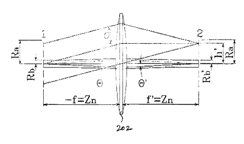
Fig. 2 explains the ATO principle through geometric optics by means of an
Angle-to-
Offset Link Lens (ATOLL). Fig. 2 shows an array of N light beams with their
waists
situated at plane 1. This array occupies a circle with a radius Ra. Each of
these beams
has the waist beam radius Rh and semi-divergence angle 8. The length of the
near-zone
of all these beams is Z"= Rb / 0. In accordance with the present invention,
any one of
these beams is to be directed to any point within a circular area with a
radius Ra in plane
2. Further, in accordance with the invention, all of these beams have their
waists at plane
2, having the same beam radius Rb and the same semi-divergence angle 0. Plane
1 is the
front focal plane of the ATOLL 202, and plane 2 is its rear focal plane. The
effective
(rear) focal length of the lens f is equal to Z", the length of the near zone
of all the light
beams.
The beam waist radius at plane 2 is equal Rb' = 0 f = 8 Z" = Rb. The beam semi-
divergence angle after the lens is 0' = R» / f = Rb / Z" = 8. Thus, the beam
waist radius
and divergence remain the same after the lens. The position of the beam axis
at plane 2 is
equal to h' _ - a f, where 6 is the beam axis tilt angle at plane 1. It is
defined entirely by
this angle, and hence by steering this angle at plane 1 within the range 06b=~
Ra / Zn , a
beam is directed to any point at plane 2 within a circle of radius Ra.
The diameter of the ATOLL 202 is chosen to be not less than DA= 2 Ra+ 2 D6 f+
20 f.
This description applies to both, mufti-mode and single-mode fiber light
beams. The
semi-divergence angle of a single-mode light beam is equal to A=~, / 7Z cn,,
The near zone
of a single-mode light beam is called Raleigh range and is equal to Z"=~ c~,2
/ ~,, where
c~, is the single-mode beam waist radius defined at the 1/e' energy level and
~, is the
wavelength.
6
CA 02326362 2000-11-20
CA 02326362 2000-11-
ATO Principle Described Through Gaussian Beam Optics
The beam power of a Gaussian beam is principally concentrated within a small
cylinder
surrounding the beam axis. The intensity distribution in any transverse plane
is described
by a circularly symmetric Gaussian function centered about the beam axis. The
width of
this function is at a minimum at the beam waist and grows gradually in both
directions.
Within any transverse plane, the beam intensity assumes its peak value on the
beam axis
and drops by the factor 1/e2 at the radial distance p = W(z). W(z) is regarded
as the beam
radius or the beam width, since about 86% of the beam power is carried within
a circle of
this radius W(z). The dependence of the beam radius on z is described by the
following
equation:
2
W(z)=Wo 1+ z
zo
The beam radius assumes its minimum value Wo in the plane z = 0 which is
called the
beam waist, and hence Wo is the waist radius. The beam radius increases
gradually with
z, reaching ~Wo at z = zo , and continues increasing monotonically with z. If
z » zo
then the first term can be neglected resulting in the following linear
relation
W(z)= wo z=9oz
zo
wherein eo = Wo / zo
zo
using Wo = ,
the following equation is obtained
8 =
o ~' Wo
Further, if z » zo , i.e. far from the beam center, the beam radius increases
approximately
linearly with z, defining a cone with half angle 60 . About 86% of the beam
power is
confined within this cone. The angular divergence of the beam is therefore
defined by
the divergence angle
7
CA 02326362 2000-11-20
-2
° ~ 2 W«
As is seen, the beam divergence is directly proportional to the ratio between
the
wavelength ~, and the beam waist diameter 2W° .
The parameter zo is known as the Raleigh range or near zone and denotes a
distance
where the area of the beam doubles. Thus,
if A~ = 2Ao
and A, =~cW,2 and Ao =~t Wo'
~ Wl 2 = 2~ W° z
W~ =~Wo
General Gaussian beam theory states that if the input waist of ~2 beam radius
W1 is
a
placed at the front focal plane of a lens of focal length F then the output
waist of ~2
a
beam radius WZ is located at the back focal plane of the lens. The
relationship between
these radius sizes is shown in the following equation
W _ F~,
Z ~ W,
It is apparent from this equation, that the input beam size and divergence
equals the
output beam size for a given focal length F. Thus, for a given focal length of
the lens, the
focal length is proportional to the square of the beam radius. This applies
also in an
analogous manner to a mirror, another element having optical power, where the
front and
back focal plane are the same.
Fig. 3 presents a basic optical system for an optical switch 200 in accordance
with the
present invention based on an Angle-to-Offset Mirror (ATOM) 210. A waveguide
bundle 220 is shown on the left of Fig. 3 with arrowheads denoting respective
interleaved
input and output ports of the switch 200. Beam directing means 230 are
provided using a
8
CA 02326362 2000-11-20
transmissive deflection mechanism in order to direct the beam to a certain
point of the
ATOM 210 so that the beam is deflected to a respective output port of
waveguide bundle
220. The beam directing means 230 are described in more detail below. It is
apparent,
that the beam can be directed to any one of the output ports of waveguide
bundle 220 by
appropriately selecting the deflection point on ATOM 210. In accordance with
the
present invention, ATOM 210 has a focal length L 240 corresponding to the near
zone
length or Raleigh range. Such an arrangement provides a compact optical system
in
which the necessary deflection angles are reduced by two and further avoids
excess
losses due to a defocusing. In order to determine the switch dimensions the
following
scaling factors are used: an F# of the ATOM 210, an area filling factor for
micro-beams
(K), and a linear number of ports (N); for example N=64 for a 4096x4096
optical switch.
The dimensions of the optical switch 200 are determined by the diameter ( ~ )
244 of the
ATOM 210
L
F#'
the divergence angle ( 8 ) 246
1
tan(9) = 4F#'
the diameter (d) 242 of the waveguide bundle 220
d - 18 (2N-1)2~ F#, and
Kit
the focal length (L) 240 of the ATOM 210
L - 36(2N-1)z~ F#2
K~
The deflection mechanism of beam directing means 230 can be an arrangement of
dual
mirrors or an arrangement of a wedge on a dual tilt mount. Fig. 19 of U.S.
Patent No.
6,101,299 illustrates such means for bi-directionally directing the beam of
light from the
input waveguides to the ATOM and from the ATOM to the output waveguides. Such
dual mirror arrangements are for example a combination of a first mirror
operable in
horizontal deflection and a second mirror operable in vertical deflection,
e.g. Fig. 3a, or a
9
CA 02326362 2000-11-20
combination of a fixed mirror as a first mirror and a second mirror that is
operable in 2D
deflection, e.g. Fig. 3b.
Alternatively, a MEMS device 300, such as shown in Fig. 4, can be used as a
transmissive deflector. This MEMS device 300 changes an axis of an optical
cone of a
beam of light emitted by the waveguide but keeps its "vertex" in place. This
change is
indicated by dotted lines in Fig. 4 and by repositioning the waveguide 312
from position
A to position B, the axis of the optical cone changes from 310a to 310b,
respectively.
Waveguide 312 is placed into a small countersunk bearing hole 314 of a top
chip 316 (Si
wafer 250 ~) of MEMS device 300. The bottom chip 318 (Si wafer 250 p) is
bonded to
the top chip 316 with solder bumps 320 (30 w), which can give interwafer
distances
controllable to submicron accuracy. The waveguide 312 passes through a hole in
this
wafer/bottom chip 318, and is engaged by an x-y positioner 322, such as a comb
drive or
a thermal drive. In order to apply a larger force on waveguide 312, two comb
drives or
two thermal drives are provided. The waveguide continues for some distance to
a strain
relief fixture 324, to avoid a possible fracture of the waveguide for example.
The
required actuation for a +/- 7 degree steering with the dimensions shown in
Fig. 4 is
about +/- 35 to 40 ~.
Fig. 5 shows another embodiment of the present invention wherein the optical
switch
500, drawn in a transmissive configuration, is based on an Angle-To-Offset
Link Lens
(ATOLL) as the element of optical power and two MEMS chips. Switch 500 has an
input waveguide bundle 510 and output waveguide bundle 512, imaging lenses
514, an
input MEMS chip 516 and an output MEMS chip 518, and an ATOLL 520. The
description presented herein only discusses the light issued from the input
bundle 510, i.e.
the input side of the system 500. Since this is a symmetric system and since
light is
generally bi-directional, the description also applies to the output side.
Each fiber end-face is imaged onto a respective micro-mirror on the MEMS chip
516
using imaging lens 514. The focal length fa of the ATOLL 520 is equal to the
near-zone
length (multimode fibers) or the Raleigh range (single mode fibers) of the
beam at the
CA 02326362 2000-11-20
MEMS plane and thus, the MEMS chips 516 and 518 are placed at the front and
back
focal planes of the ATOLL 520, as shown in Fig. 5. By properly directing two
micro-
mirrors of the two MEMS chips 516 and 518, a link between any two waveguides
from
the input waveguide bundle 510 to the output waveguide bundle 512 is
established.
Thus, the MEMS chips 516 and 518 fulfil the function of beam directing means.
The
micro-mirrors on the MEMS chip 516 introduce a tilt of each input beam which
is
converted to a lateral displacement with the same mode size through the ATOLL
onto a
set of output micro-mirrors on the second MEMS chip 518 which redirect these
beams to
a the outputs at the output waveguide bundle 512. The range of the mirror
steering is
one-half the range of the beam steering as shown in the following equation,
see also the
section describing the ATO principle through geometric optics,
Dab=~ Ra / 2 Z" .
The beam axes between the input waveguide bundle 510 and imaging lens 514 are
parallel to each other, or telecentric; however, they cease to be telecentric
as they
propagate from the imaging lens 514 to the MEMS chip 516. The skew angle of
the
beam axis after lens 514 is a' = h / f , where h is one-half of the size of
the waveguide
bundle, or expressed alternatively, the height of the fiber bundle from the
optical axis.
Therefore, the skew angle needs to be compensated by non-uniform tilting of
each micro-
mirror on the MEMS chip 516 which results in an increase of the required angle
of mirror
steering. However, it is desirable to minimize the total required angle of
micro-mirror
deflection, and in accordance with a further embodiment of the present
invention a
second magnifying system is included in order to image the beams from the MEMS
chip
to the ATO lens. The use of a second magnifying lens provides additional room,
if
needed, and magnification to increase the mode size in the case that the focal
length of
the ATO lens 520 is too small. However, it is advantageous to replace lenses
514 with a
telecentric 4-f relay magnifier. Replacing lenses 514 by telecentric systems
of the same
magnification ensures a telecentricity of the beam axes as they approach the
MEMS chip
which obviates an increase in the range of mirror steering. In this case the
range of
mirror steering remains the same as it was described above with the following
equation
Dab-~ Ra / 2 Zn.
11
CA 02326362 2000-11-20
Fig. 6 shows another autocollimative/reflective optical switch 600 based on a
focusing
Angle-To-Offset Mirror (ATOM). Its operation is similar to the optical switch
200
described in conjunction with Fig. 3. However, switch 600 employs a MEMS chip
614
having a micro-mirror arrangement thereon for directing the beam to a
respective
deflection point on the ATOM 616. Aside from the ATOM 616, switch 600 has a
waveguide bundle 610, a projective lens 612, and a MEMS chip 614. Again, it is
advantageous to use a telecentric magnifier for the projective lens 612. Input
waveguides
and output waveguides are mixed together in waveguide bundle 610 and hence,
the port
count of optical switch 600 is reduced by a factor of 2. In accordance with
this
embodiment of the invention, the micro-mirrors on the MEMS chip comprise the
micro-
mirrors dedicated for directing the input signals as well as the output
signals. The layout
of the micro-mirrors on the MEMS chip 614 depends on the assignment of the
input port
or ports and the output ports on the waveguide bundle 610, i.e. whether they
are sectioned
in groups or interlaced, for example.
Figs. 7 to 11 illustrate further design considerations for optical switches in
accordance
with the present invention. The number of ports is defined by the imaging
lens, the size
of the MEMS chip, and the ATO lens or mirror. The number of ports that can be
accommodated in the optical system is directly proportional to the size of the
MEMS
chip, inversely proportional to the F/#, and proportional to the square of the
optical filling
factor. Thus, in order to maximize the port count, it is most efficient to
maximize the
optical filling factor.
The optical filling factor is defined as follows Kf= Db / D;, where Db is the
beam
diameter and D; is the distance between the axes of two closest beams. Since
the
diameter of a standard single-mode fiber is 125 ~m and its mode field diameter
is
~15~m, which is defined at the level 3c~, the filling factor of the waveguide
bundle can
not be higher than 0.12. This optical filling factor is not effected by the
magnification
through the magnifying lens at the MEMS chip. However, below some techniques
are
described that can be used to increase the filling factor.
12
CA 02326362 2000-11-20
A first technique for increasing the filling factor is to place an array of
micro-lenses on
top of the waveguide bundle end-face; one micro-lens centered on the optical
axis of each
waveguide. Such micro-lenses increase the beam diameter but not the distance
between
the beam axes and thereby directly improve the filling factor.
Fig. 7 demonstrates a second technique for increasing the filling factor which
is to draw
the fiber bundle under high temperature. The drawing diminishes the size of
the bundle
cross-section keeping geometrical similarity of original and drawn cross-
sections. The
drawing factor is defined as Kd = Dd / Db, where Db is the bundle diameter of
the original
bundle, and Dd is its diameter after drawing.
The distance between fiber axes diminishes and so does the fiber core
diameter. The
mode field radius c~ dependence on step-index single-mode fiber core diameter
is given
by Marcuse's formula:
co = D (0.65 + 1.619 V-is + 2.879 V-6) /2
where normalized frequency V = D~ yl~ - ylz l'~ , W and n2 are refractive
indexes of the
fiber core and cladding, and D is the fiber core diameter. A mode field radius
dependence on the drawing factor Kd for SMF-28 single-mode fiber is calculated
according to this formula and this dependence is presented in Fig. 8, together
with the
filling factor dependence.
Looking at the graph presented in Fig. 8 from right to left, it is seen that
the mode
diameter remains approximately the same down to a drawing factor ~ 0.85, and
then
increases, while the filling factor increases monotonically as a function of
the drawing
factor.
A third possible technique for increasing the filling factor is to use a so-
called "parallel
projection" where several waveguide bundles, e.g.910 and 920, and associated
projecting
lenses 915 and 925 image the inputs from several locations for each MEMS chip
930.
Such a "parallel projection is shown in Fig. 9, which is a modification of the
system
13
CA 02326362 2000-11-20
presented in Fig. 6, i.e. the reflective configuration. A similar modification
can be done
with the system presented in Fig. 5, i.e. the transmissive configuration.
In this parallel projection scheme, there are four sub-systems consisting of
waveguide
bundles 910 and 920 and projecting lenses 915 and 925 placed around an ATOLL
(not
shown) or an ATOM 940. Each of these sub-systems projects the light from its
corresponding waveguide bundle 910 and 920, respectively, onto the same MEMS
chip
930. Each image is oriented such that it is shifted relatively from its
neighbour by half a
pitch in one of the possible directions, see Fig. 10. Such a honeycomb
structure can be
used for the placement of waveguides and micro-mirrors of MEMS chips, as it
provides
the most compact positioning and the biggest number of connected channels.
With the parallel projection scheme shown in Fig. 9, the filling factor is
increased two
times. If nine parallel sub-systems are placed around the ATO mirror 940 or
ATO lens
(not shown), the filling factor is increased 3 times; by using 16 systems, the
filling factor
is increased 4 times and so forth.
Using this technique implies requirements for increased steering range of
micro-mirrors,
since they should compensate the angle between optical axes of projecting
systems and
the axis of the ATOLL or ATOM.
It is apparent that such a configuration lends itself as an example of how
this system is
built modularly, growing in port counts as desired or required by the
customer.
A fourth possible technique to improve the filling factor is to etch away some
of the
cladding of the fibers.
As illustrated above, it is necessary to clock the MEMS chip with respect to
the optical
axis of the imaging lens. This is necessary to deflect the beams to propagate
down the
optical axis of the ATO lens or mirror. As a result of this, not all of the
micro-mirrors are
positioned at the image plane of the imaging system. Although this does not
constitute a
14
CA 02326362 2000-11-20
theoretical problem, there could be practical issues associated with this,
such as skew
rays or missing micro-mirrors. In this case, larger micro-mirrors are
necessary to capture
the converging or diverging beams, for example.
In order to prevent this problem, an alternate optical scheme 1100 is
presented in Fig. 11
in a transmissive configuration, wherein the telecentric imaging lens 1110 is
itself not
axially co-linear. The ATOLL is denoted with 1125 and the output waveguides
are
denoted with 1115. With this scheme, it is seen that the images of each input
waveguide
1105 are co-planar with the MEMS chip 1120. However, if desired, this scheme
is
designed in reflection. Optical system 1100 requires greater care in the
design of the off-
axes lenses in order to avoid problems with aberrations of the lenses.
Numerous other embodiments can be envisaged without departing from the spirit
and
scope of the invention.
CA 02326362 2000-11-20
I1-2f3-00 15:52 JDS FITEL Inc. ID=1 613 823 4985 P01/13
-~. D '.~ ~ ~~ crt.e~~a ~~
.L h p~~ ~ -~-p.
r a ~C ' ~ ~"~ ~ ~ ~~
.
due.-:- 'o~ ~..s.... '(~.,,~ n~r~-~- ~"~ ~'~ ~--~ S ~~ ~'"~
a
r
r
Q ~~ ~
c~... ~. ~ ~..~.~.~ ~ ~ ~-'~'a C~ . ~r , ~
r.. P ,.~,,.~.~ ~ ~'
°~ ~
-. .
r °~
r
~G ~ w~~
... P
s
2 ~.~,.
.- ~-~.
r.
",. . -rte.
e...
._--
CA 02326362 2000-11-20
LI-20-00 15:52 JDS FITEL Inc. ID=1 613 823 4985 P02i13
'., a~.~: s~.t. d~ - I,..~.C,~ Sr.' ~ , ~~d ~e~~ v~~~ ~'r:~t"" '~
~''~.,~c ~,' V t
o"., d ~,.~. _ a,,,. dv~.c~
~c ~c . ~"''-.
-.,;~C ~. ~-tw~
.. ,",
a
w.rc~ .~e.. -~,.,~ ~ ~~ .
CA 02326362 2000-11-20