Note: Descriptions are shown in the official language in which they were submitted.
CA 02326664 2000-10-02
WO 99/52289 PCT/US99106723
APPARATUS AND METHOD FOR CONTROLLING TRANSFER OF DATA
BETWEEN INTERCONNECTED DATA PROCESSING ELEMENTS AND
PROCESSING OF DATA BY THESE DATA PROCESSING ELEMENTS
FIELD OF THE INVENTION
The present invention is related to apparatus and methods for controlling
transfer and
processing of data by interconnected data processing elements. The invention
is more
particularly related to the processing of temporally continuous media data,
including motion
video and audio data.
BACKGROUND
Analog motion video signals, such as those used in common television sets,
video tape
recorders and other analog video systems, are temporally continuous and
synchronous signals
requiring various elements in a video system to be synchronized in order to be
used. In other
words, analog motion video signals have a predetermined and fixed rate to
which all of the
elements in the video system are synchronized. Any element in the video system
is designed
with the assumption that there will be a constant rate for input and output of
motion video
information.
More recently, it has been possible to store digital motion video data in data
files on a
2o computer. There are several methods for playing back such motion video
data. One method
is called "pushing" or "streaming" of the motion video data. Streaming is
based on an
assumption that a system can provide an average data flow rate that is the
same as the ultimate
data flow rate needed to ensure temporally continuous output of analog motion
video images
to a viewer. Sufficient buffering is used to account for expected latencies in
data transfer
between elements. In some cases, both the temporal and spatial resolution of
the motion
video information may need to be reduced. Such systems typically are designed
with the
assumption that transfer of audio and video data from a source through several
processing
elements to its ultimate destination can neither be delayed nor stopped.
When a general purpose digital computer is used to process motion video
information,
3o a constant rate of flow of data generally cannot be maintained. There may
be variations in
data flow rates due to various latencies in the computer system due to, for
example, disk or
memory read latency, interrupts from other processing elements in the
computer, etc. In
addition, in some systems, such as editing systems, the ability to stop and
restart playback is
CA 02326664 2000-10-02
WO 99/52289 PCT/US99/06723 -
-2-
desirable. In order to overcome such problems, one method which has been used
is to provide
sufficient buffering in combination with an ability for data transfer to be
stalled, such as
shown in U.S. Patent No. 5,045,940 (Peters, et al.) which is hereby
incorporated by reference.
These principles are used in a computer network as described in published
European Patent
Application No. 0674414A2. An extension of this combination to special effects
processing
is disclosed in PCT Publications W094/2481 S and W095/26100 which are
incorporated by
reference. In this system, a data decompressor outputs data into a first
buffer, from which it is
transferred to a second buffer associated with a special effects processor.
The first buffer
indicates whether valid data is available. In addition, the special effects
processor indicates to
1 o a controller associated with the decompressor whether it can receive data
based on memory in
the second buffer.
One drawback of these systems is that they use a significant amount of
buffering to
accommodate for delays in data transfer between elements. They also are
generally designed
for use with a single predetermined format of media. The data transfer
protocol also may
15 involve tightly coupled handshake signals between the sender and the
receiver of data.
SUMMARY
An interface enables asynchronous data processing elements to be
interconnected
using an interconnection protocol that controls the flow of data between the
processing
2o elements. The flow control allows the processing elements to be data
independent, i.e., the
processing elements need not be designed for a fixed sample rate or
resolution, sample format,
or other data dependent factors. When used with digital motion video data, the
processing
elements may process motion video data at various temporal and spatial
resolutions and color
formats and precisions. Flow of data between processing elements may be
controlled by
25 handshake signals indicating whether the data output by the sender is valid
and whether the
receiver can receive data. The sender transmits data and asserts a valid data
signal along with
the data in response to a request signal from the receiver. The request signal
may be asserted
by the receiver and responded to asynchronously by the sender with the
transmission of the
data by the sender. As a result, the sender and receiver are decoupled, thus
enabling high
3o speed data transmission and time division multiplexing of data across the
interconnect. The
sender also may transfer command data. A valid command signal is used to
indicate the
presence of command data on the interconnect.
CA 02326664 2000-10-02
WO 99/52289 PC'f/US99/06723 -
-3-
Accordingly, in one aspect, an output interface for a sender of data has an
output for
providing a datum and a boundary signal indicating whether the datum defines a
boundary of
a sample of the data and a valid data signal associated with a datum and
indicating whether
the associated datum is valid. An input provides a request signal from a
receiver indicating
a request for transfer of data from the sender. A controller, after receipt of
the request
signal, directs data to the output and that asserts the valid data signal in
association with the
datum.
In another aspect an output interface for a sender of data has an output for
providing a
datum and a boundary signal indicating whether the datum defines a boundary of
a sample of
to the data and a valid data signal associated with data and indicating
whether the associated data
is valid and a valid command signal associated with a command data and
indicating whether
the associated command data is valid command data. An input provides a request
signal
from a receiver indicating a request for transfer of data from the sender. A
controller
transfers data with one of the valid data signal and the valid command signal
asserted when
a request signal is received.
In one embodiment, the output further provides a reference clock signal and
the data
is output by the output interface at a rate defined by the reference clock.
The output may
have data lines for carrying the datum, a boundary signal line for carrying
the boundary
signal, and a valid data signal line for carrying the valid data signal. The
input may include
2o a request signal line for carrying the request signal.
In another embodiment, the output includes a valid command signal associated
with
a datum and indicating whether the associated datum is valid command data. The
controller,
after receipt of the request signal, directs command data to the output and
asserts the valid
command signal in association with the datum. The output interface also may
encode
packets of data using a combined state of the valid data signal and the valid
command
signal.
In another embodiment, the output interface may have a phase-lock loop having
an
input for receiving the reference clock and an output providing a clock signal
having a rate
higher than a rate of the reference clock. The rate defined by the reference
clock for
3o receiving data is the rate defined by the output of the phase-lock loop.
When the rate of the
output of the phase-lock loop is a non-integer multiple of the rate of the
reference clock, the
output interface synchronizes the phase-lock loop with a phase-lock loop in an
input
CA 02326664 2000-10-02
WO 99/52289 PCT/US99/06723 -
-4-
interface receiving the data from the output interface. Time division
multiplexing of data
onto the output interface at the rate of the output of the phase-lock loop may
be performed.
In another embodiment the output interface may include a counting circuit
having a
f rst input for receiving a value to be loaded to provide an output, wherein
the output
indicates a number of samples of the processed data for which the command data
is valid,
and control logic for tracking a number of samples processed by the processing
element and
for generating the control signal to the processing element after the
processing element
outputs the last sample for which the command data is valid.
In another aspect, an input interface for a receiver of data has an input for
receiving
1 o from a sender a datum and a boundary signal indicating whether the datum
defines a boundary
of a sample of the data and a valid data signal associated with a datum and
indicating whether
the associated datum is valid. An output provides a request signal indicating
a request for
transfer of data from the sender. A controller issues the request signal when
the input
interface is capable of receiving data and reads the datum from the input when
the valid
t 5 data signal in asserted.
In another aspect, an input interface for a receiver of data, has an input for
receiving
from a sender data and a boundary signal indicating whether the data defines a
boundary of a
sample of the data and a valid data signal associated with the data and
indicating whether the
data is valid and a valid command signal associated with the data and
indicating whether the
2o data is valid command data. An output provides a request signal indicating
a request for
transfer of data from the sender. A controller issues the request signal when
the input
interface is capable of receiving data and reads the datum from the input when
one of the
valid data signal and the valid command signal is asserted.
In one embodiment, the input further receives a reference clock signal and the
data
25 is read by the controller at a rate defined by the reference clock. The
input may include
data lines for carrying the datum, a boundary signal line for carrying the
boundary signal,
and a valid data signal output line for carrying the valid data signal. The
output may
include a request signal line for carrying the request signal.
In one embodiment, the input further receives a valid command signal
associated
30 with a datum and indicating whether the associated datum is valid command
data. The
controller issues the request signal when the input interface is capable of
receiving data and
reads the command data from the input when the valid command signal in
asserted. The
CA 02326664 2000-10-02
WO 99/52289 PCT/US99/06723 -
-5-
input interface also may decode packets defined by a combined state of the
valid data signal
and the valid command signal.
In one embodiment, the input interface further includes a phase-lock loop
having an
input for receiving the reference clock and an output providing a clock signal
having a rate
higher than a rate of the reference clock. The rate defined by the reference
clock for
reading data is the rate defined by the output of the phase-lock loop. When
the rate of the
output of the phase-lock loop is a non-integer multiple of the rate of the
reference clock, the
input interface synchronizes the phase-lock loop with a phase-lock loop in an
output
interface of the sender providing the data to the input interface. The input
interface also
1o may demultiplex time division multiplexed data on the input interface using
the output of
the phase-lock loop.
In another embodiment, the input interface further includes a counting circuit
having
a first input for receiving a value to be loaded to provide an output, wherein
the output
indicates a number of samples of the processed data for which the command data
is valid,
~ s and control logic for tracking a number of samples processed by the
processing element and
for generating the control signal to the processing element after the
processing element
outputs the last sample for which the command data is valid.
In other aspects, an integrated circuit for processing data, particularly
video data, may
contain an input interface or output interface as described above. Another
aspect is a system
20 of devices interconnected using input and output interfaces as described
above. Another
aspect is a process performed by an output interface and its various
embodiments, by which
data is transferred in response to a request signal. Another aspect is the
process performed by
the input interface and its various embodiments, by which data is captured
when an asserted
valid data signal or valid command signal is received. It should be understood
that the various
25 combinations of these embodiments are aspects of the invention.
BRIEF DESCRIPTION OF THE DRAWINGS
In the drawings,
Fig. 1 is an illustration of signals connecting two asynchronous video
processing
3o elements in an interface in one embodiment;
Figs. 2A-2G are timing diagrams illustrating the relationship of signals on
the
interface of Fig. 1;
CA 02326664 2000-10-02
WO 99/52289
PCT/US99106723
-6-
Figs. 3A-3C are block diagrams of three embodiments of a processing element
having
an output providing the signals described in Fig. 1 and Figs. 2A-2G;
Fig. 3D is a state diagram of a flow control process performed by a sender of
data;
Figs. 4A-4D are block diagrams of three embodiments of processing elements
having
inputs corresponding to the signals shown in Fig. 1 and Figs. 2A-2G;
Fig. S is flow chart describing how a phase-lock loop at a sender is
synchronized with
a phase-lock loop at a receiver;
Fig. 6 is a flow chart describing how a phase-lock loop at a receiver is
synchronized
with a phase-lock loop at a sender;
1o Fig. 7 is a timing diagram illustrating time division multiplexed channels
on an
interconnect;
Fig. 8 is a timing diagram illustrating time division multiplexed channel
sets;
Fig. 9 is a block diagram of a multichannel time division multiplexed
interconnection
of devices;
15 Fig 10 is a block diagram illustrating a single time division multiplexed
connection;
and
Fig. 11 is a more detailed block diagram of the request signal demultiplexer
and
synchronizer shown in Fig. 10.
2o DETAILED DESCRIPTION
An asynchronous data interface interconnects processing elements in a manner
which
allows the processing elements to be data independent. For example, for
digital motion video
data the interconnect allows for format independence, temporal and spatial
resolution
independence, frame rate independence and variability, and faster than real-
time transfer of
25 compressed or uncompressed digital motion video data between processing
elements. In
general, the interface allows processing elements to treat media as computed
data rather than
temporally continuous data. Because of the data independence of both the
interconnect and
the processing performed by interconnected processing elements, different
formats of data and
different media types may be multiplexed with different bandwidths across the
same
3o interconnect. An assumption that motion video data and audio data cannot be
burst across an
interconnect may be eliminated. Motion video data therefore can be processed
with
processing elements that allow for multiple temporal and spatial resolutions,
color and pixel
CA 02326664 2000-10-02
WO 99/52289 PCT/US99/06723 -
-7-
representations and resolutions, full motion and less than full motion video,
broadcast quality
and less than broadcast quality video data, and multiplexing of two or more
data streams
including video data, key data, other kinds of data and commands over the same
interconnect.
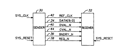
Fig. 1 illustrates an interface between a sender and a receiver of data. The
sender and
the receiver may be implemented as separate integrated circuits or by separate
discrete
devices. A sender 30 is connected to a receiver 32 through a data interconnect
34 that carries
data (DATA(9:0)) between devices. Although this embodiment is described in
connection
with 10-bit video data, other kinds of data end data previsions may be used.
Such data
includes, but is not limited to video data, key data, audio data, command or
other data. The
1 o data type either may be agreed upon either by convention or by signals
labeled in the data
stream, or may be specified by command data. 'The interface is unidirectional,
but the
direction may be selectable under appropriate software and/or hardware
control.
Data from a sender on this video data interface may be relative to an edge,
e.g., the
rising edge, the falling edge or both, of the interface clock (CI;K), e.g., a
twenty-seven
15 megahertz (27 MHZ) clock provided on a signal line 42. The interface clock
may be
established either by an external source or by the sender, e.g., when source
synchronous
clocking is used to transmit data over long distances. Data from a receiver
(e.g., a REQ~N
signal) is asynchronous to the reference clock, unless the reference clock is
used for timing of
time-division multiplexing, as described below.
20 The precision, in bits, of the data interconnect 34 of the interface
depends on the
application. For example, motion video data may use 8-bit, 10-bit , 12-bit and
16-bit and
other precision data paths. In such an embodiment, the interface may be a
single video
component in width, according to an appropriate video format convention. For
example,
chroma and lama samples alternating on successive clocks following a 4:2:2
convention
25 (CCIR601 ) may be supported. Other example formats include, but are not
limited to, RGB,
4:4:4, RGBA, 4x4 and 4:2:2:4. In general, the interface is format independent
so long as the
sender and receiver agree to or specify the selected format. When a 10-bit
interface is used for
8-bit video data, the least significant bits (DATA 1:0) may be left undefined,
or may be
defined by convention in an application. For example, for SMPTE-compliant
data, these least
3o significant bits should be set to zero. 10-bit data also may be sent over
an 8-bit interconnect
using a data packing protocol described in U.S. Patent Application entitled
"Video Data
Storage and Transmission Formats and Apparatus and Methods for Processing
Video Data in
CA 02326664 2000-10-02
WO 99/52289 PCTNS99/06723 -
_g_
Such Formats," filed April 3, 1998, by Craig R. Frink, Raymond D. Cacciatore
and Hamed
Eshraghian, which is hereby incorporated by reference.
The flow of data from the sender 30 to the receiver 32 across the data
interconnect 34
may be controlled using two handshake signals. The first handshake signal is a
request signal
(REQ-N) sent across a signal line 38 from the receiver. The request signal is
generated by the
receiver to indicate its ability to accept new data, which also allows the
receiver to pace the
flow of data. The request signal also may be asserted by the receiver
independent of the
second handshake signal, called the valid data signal. The valid data signal
(DVAL I~ is sent
over a signal line 40 from the sender. The valid data signal is associated
with a datum at the
sender and indicates whether the associated datum is available to be
transferred. The valid
data signal may be asserted by the sender in response to the request signal.
The sender uses
the valid data signal to control the flow of information to the receiver.
A boundary signal (BNDRY N), sent by the sender across a signal line 36 with
the
data to the receiver, represents auxiliary information about the data
transferred across the
interface. This boundary signal signifies at least the boundary of data for a
given sample,
which is defined by convention for an application between a sender and
receiver. For
example, for motion video data the boundary signal may designate an image
boundary, or
another boundary such as a line or pixel or video datum such as a component.
When used to
designate an image boundary, this signal may be asserted at the same time the
data for the last
2o component of either a pixel in the image or a key is on the data
interconnect 34 in order to
indicate the end of the image. The start of data for a sample, such as an
image, may be
signaled instead of the end. The boundary signal also may be encoded such that
a transition in
the signal designates an end of field and the state of the signal on the first
component of the
field indicates the sense, i.e., odd or even, of the field. The auxiliary
information also may
indicate the presence of data of a particular type or command data. The
boundary signal is
asserted with the same timing as the data on the data interconnect 34 and
follows the same
flow control behavior as the data. It may be valid when the valid data signal
is asserted.
A valid command signal (CVAL N) also may be sent by the sender across a signal
line 44. The valid command signal indicates the presence of command data on
the interface.
3o Similar to the valid data signal, the valid command signal is associated
with a datum at the
sender and indicates whether the associated datum is valid. The valid command
signal may
be asserted by the sender in response to the request signal. In one
embodiment, the valid
CA 02326664 2000-10-02
WO 99/52289 PCT/US99/06723 -
-9-
command signal may be asserted independent of the request signal. In that
embodiment, the
receiver has a buffer for receiving the command data. The sender uses the
valid command
signal to control the flow of command data to the receiver.
Another way to provide command data to a device is by loading control
registers
through another interface. A counting circuit may be used to specify the
number of data
samples to which the command data is valid. This counting circuit may be
decremented by a
boundary signal in the interconnect. Pre-roll and post-roll operations may be
performed using
a similar counter. Such a counter is described in U.S. Patent Application
Serial No.
08/879,981, entitled "Apparatus and Method for Controlling Transfer of Data
Between and
1o Processing of Data by Interconnect Data Processing Elements," by Jeffrey D.
Kurtze et al.,
which is hereby incorporated by reference.
Timing diagrams illustrating the flow of data across the connection will now
be
described. The interconnect supports both constant flow and controlled flow
connection
protocols over the interconnect. In a controlled flow application, the
handshaking signals (the
valid data signal, valid command signal and the request signal) are used to
manage the flow of
data. Either the sender or the receiver can control the flow. A constant flow
application is
one in which the flow of data is generally not stopped, for example, for a
connection to a
video camera or a video playback device. In the constant flow mode of
operation, the request
signal does not have the same significance, insofar as the request signal is
considered asserted.
2o However, the valid data signal is still used to indicate valid data on the
interconnect. For
example, the valid data signal may correspond to the active video portion of a
video signal
when transmitting video data.
In controlled flow operation, the receiver indicates its ability to accept
data by
asserting the request signal. The request signal may be considered a stop
signal. When the
request signal is not asserted, the signal indicates that the sender should
stop sending data to
the receiver. The sender asserts either the valid data signal or valid command
signal
coincident with the data in response to the request from the receiver. This
protocol permits
variable length delays between the assertion of the request signal by the
receiver and the
receipt by the receiver of the valid data signal or valid command signal from
the sender. This
3o delay decouples the sender and receiver, allowing controlled flow of data
over large distances
without complex timing considerations and with high performance. In this
protocol, the valid
data signal or valid command signal and accompanying data are forwarded in
response to a
CA 02326664 2000-10-02
WO 99/52289 PCT/US99/06723 -
- 10-
request signal. The sender considers a request signal a "permission to send"
signal and an
indication of the ability of the receiver to accept new data. The receiver
uses the valid data
signal and the valid command signal to qualify the data. on the interconnect.
Data not
captured by the receiver when either the valid data signal or the valid
command signal is
present results in loss of the data. The signal timing, as discussed above, is
controlled by the
reference clock.
In constant flow connections, the receiver guarantees that it captures valid
data when
present on the interconnect. The sender assumes that the request signal from
the receiver is
asserted. In these connections, the sender asserts the valid data signal for
data to be captured
I o at the receiver. A clock period of the reference signal might not
correspond to valid data, and
thus the valid signal sometimes is not asserted.
In this example and in those to follow, the request signal (REQ N), the valid
data
signal (DVAL N), the valid command signal (CVAL N) and the boundary signal
(BNDRY N) are negative logic signals.
Referring now to Fig. 2A, a simple data transfer example will now be
described. In
Fig. 2A, a clock signal 50 represents the interface clock applied to the clock
inputs of the
sender and receiver. Data are shown at 52. The valid data signal is shown at
54 and the valid
command signal is shown at 56. The request signal is shown at 58. The boundary
signal is
shown at 60. The boundary signal 60 and a valid command signal 56 are shown
unasserted
2o for simplicity of illustration. The request data signal 58 is shown
asserted in clock cycle 53.
In response, in the next clock cycle 55, the sender asserts the valid data
signal 54 and outputs
valid data 52. As shown in this example, the request signal indicates whether
the receiver is
able to accept data from the data interconnect. The sender outputs valid data
and asserts the
valid data signal after receipt of a request signal. There may be a one or
more clock cycle
delay between the receipt of a request signal and the output of a valid data
signal. Data is read
from the data interconnect by the receiver when the valid data signal is
asserted. The request
signal might not be asserted at the receiver when valid data is ultimately
received.
An alternative embodiment is shown in U.S. Patent Application Serial No.
08/879,981, in which data is transferred when the request signal and valid
data signal are
3o asserted during the same clock cycle. Another embodiment is shown in U.S.
Patent
Application entitled "A Packet Protocol for Encoding and Decoding Video Data
and Data
Flow Signals and Devices for Implementing the Packet Protocol," filed April 3,
1998, by
CA 02326664 2000-10-02
WO 99/52289 PCT/US99/06723 -
-11-
Craig R. Frink and Andrew V. Hoar, which is hereby incorporated by reference,
in which
packets of data are transmitted and a receiver transmits a request packet
indicating an amount
of data.
Fig. 2B is a timing diagram illustrating control of the flow of data by the
sender using
the valid data signal. The sender uses the valid data signal to indicate valid
video or key data
that is available to be read by the receiver from the interface. The data is
valid when the valid
data signal is present and the data is lost unless the receiver accepts the
data during the clock
cycle. The sender negates the valid data signal when valid data is not present
on the
interconnect. To simplify illustration, the boundary signal 70 and the valid
command signal
66 are shown unasserted. The valid data signal 64 is asserted for clock cycle
63, 65 and after
clock cycle 69. Accordingly, valid data is present at the video data
interconnect only when
the valid data signal is asserted (cycles 63, 65 and 69+). In this example, it
is assumed that
the request signal becomes asserted in clock cycle 61 such that the sender now
may start
sending data in the clock cycle 63. Accordingly, the receiver receives data in
clock cycle 63,
65 and 69+ of the reference clock. This timing diagram is typical of the
controlled flow
operation embodiment. In another embodiment, described in U.S. Patent
Application entitled
"Method and Apparatus for Controlling Data Flow Between Devices Connected by a
Memory," filed April 3, 1998, by Craig R. Frink, which is hereby incorporated
by
reference, the sender indicates to the receiver an amount of valid data which
is available in a
memory.
A timing diagram illustrating control of data transfer by the receiver using
the request
signal will now be described in connection with Fig. 2C. The request signal
indicates whether
the receiver is able to receive data from the data interconnect. Data is read
from the data
interconnect by the receiver when the valid data signal is asserted during a
cycle of the
interface clock. It is possible for the request signal not to be asserted when
the valid data
signal is asserted. Nonetheless, the receiver still reads data from the data
interconnect. In the
timing diagram in Fig. 2C, a clock signal 50 represents the interface clock
applied to the clock
inputs of the sender and receiver. Data are shown at 72. The boundary signal
80 and the valid
command signal 76 are shown not asserted for simplicity. The valid data signal
74 is asserted
only when valid data is on the interconnect. The request signal 78 is
initially asserted, then is
not asserted for one clock cycle 75, then is asserted for the remaining clock
cycles. When the
request signal is not asserted in any clock cycle, e.g., clock cycle 75, in
the subsequent clock
CA 02326664 2000-10-02
WO 99/52289 PCT/US99/06723 -
-12-
cycle, e.g., clock cycle 79, the data 72 on the data interconnect is indicated
as invalid by
deasserting the valid data signal 74. In this example, a two clock cycle delay
when stalling
the flow of data from the sender indicates that the receiver buffers
additional data after it
deasserts the request signal.
Figs. 2D and 2E are timing diagrams representing how the boundary signal is
used to
indicate the last component of a sample. The boundary signal may represent,
for example, a
field boundary called a vertical synchronization signal in a synchronous video
system, or
other boundary, such as a frame or line of data. The boundary signal is
asserted in
conjunction with the last component in a video or key sample. It also may be
used simply to
1o delineate command data. It is asserted with the same timing as the video
data and follows the
same flow control behavior as the video data, but its relative position with
respect to the data
is application dependent. In Fig. 2D, the data on the interconnect is
illustrated at 82. Both the
valid data signal 84 and the request signal 88 are asserted. The valid command
signal 86 is
shown unasserted for simplicity of illustration. As indicated at 90, at the
fifth clock cycle 89,
i 5 the data on the data interconnect is a component "yLnsT" and is the last
pixel component of the
last pixel of a field or frame. The pixel data on the interconnect 82 is
concurrent with the
boundary signal on the interconnect.
Referring now to Fig. 2E, if the request signal 96 is deasserted and
recognized by the
sender at the time when the boundary signal 98 is asserted, the boundary
signal remains valid
2o until the valid data signal is asserted as shown at 94. In this example, in
clock cycle 93 the
request signal is deasserted. Accordingly, in clock cycle 95, the valid data
signal is
deasserted, and the boundary signal becomes asserted. In clock cycle 97, the
request signal
again becomes asserted and the valid data signal becomes asserted in clock
cycle 99 to output
the last or boundary component. In clock cycle 100, the valid data signal and
the boundary
25 signal 98 are deasserted.
A use of the valid command signal will now be described in connection with
Figs. 2F
and 2G. The valid command signal indicates the presence of command data on the
interface.
Command data may be used to specify processing parameters, switching state,
addresses or
other information to a receiver. The use of this signal in combination with
the valid data
3o signal can indicate four states of the interconnect. Refernng to Fig. 2F,
the combination of the
valid data signal and the valid command signal may be used to indicate the
presence of the
packet of data on the interconnect. In particular, in one embodiment, the
valid data signal 102
CA 02326664 2000-10-02
WO 99/52289 PCTNS99/06723 -
-13-
when paired with the valid command signal 104 may indicate an idle state 106,
a header 108
of a packet, packet data 110, and a packet tail 112. The valid command signal
also may
observe the same protocol as the valid data signal. When the valid command
signal is
asserted, the receiver accepts data. When the receiver deasserts the request
signal, the sender
similarly deasserts the valid command signal as soon as possible. Note that in
Fig. 2F, where
the valid data and valid command signals are used in combination, the receiver
receives the
packet header, packet data and packet tail. The valid command signal also may
be used in an
interface as described in U.S. Patent Application Serial No. 08/879,981.
Referring to Fig. 2G, the boundary signal 128 is shown unasserted for
simplicity. In
1o this example, the request signal 126 is asserted in clock cycle 121. In
clock cycle 123,
command data is available on the data interconnect 120 and the valid command
signal 124
becomes asserted. In clock cycle 125, the valid data signal 122 is asserted,
the valid
command signal is deasserted and data is now available on the interconnect
120. As an
alternative, the valid command signal, when asserted alone such as shown at
123 in Fig. 2G,
may be used to indicate the presence of valid command data on the
interconnect.
Figs. 3A through 3C illustrate different embodiments of a sender device having
an
interconnect in accordance with the protocol described above. In general, the
sender has a
processing element 200 which provides the reference clock 210 as well as data
212, valid data
signal 2I4, and boundary signal 216. The data, valid data signal and boundary
signal are
2o provided to their own latches 218, 220 and 222 which are synchronized to
the reference clock
210. The output of latch 218 provides the output data 224. The output of latch
220 provides
the output valid data signal 226. The output of latch 222 provides the output
boundary signal
228. The request signal 230 received by the sender is synchronized using a
synchronization
circuit 232 to the reference clock 210. The synchronized request signal 234 is
received by the
processing element 200. The processing element also has a reset input 236 to
be described in
more detail below. In this embodiment, the valid command signal is not present
and data is
transmitted at the rate of the reference clock. The registers 218, 220 and 222
may be replaced
by a first-in/first-out memory or other storage device. In one embodiment, the
reference clock
is a 27 MHz clock which allows a standard SDTV 4:2:2 video stream to be
transmitted.
3o It is possible to transmit higher bandwidth data streams while maintaining
a reference
clock at a lower frequency by using a phase-lock loop (PLL) at both the sender
and receiver
ends of the interface. An embodiment of a sender having a PLL is shown in Fig.
3B. This
CA 02326664 2000-10-02
WO 99/52289 PCf/US99/06723 -
-14-
circuit has a phase-lock loop (PLL) 238 of which the output signal 240 is used
to drive latches
2I8, 220 and 222. The phase-lock loop outputs a signal which is a multiple of
the reference
clock. This signal is a high speed data clock that synchronizes the data at
either end of the
interface. The base frequency is transmitted over the interconnect as the
reference clock to be
used as a phase-lock loop reference at the receiver. There are several
instances where this
type of clock would be useful. For example, if the reference clock is 74.25
MHz, the phase-
lock loops may allow data transmission at a rate of 148.5 megabytes per
second, allowing
transmission of an HDTV stream. A 4:4:4:4 data stream may be transmitted at 54
MHz with
the reference clock at 27 MHz. In another embodiment, the reference clock may
have a
to frequency of 27 MHz and the phase-lock loop may be run at five and a half
times the
reference clock frequency, to produce a data rate of 148.5 MHz. In this
embodiment, the
system runs at the standard SDTV clock rate, but allows transmission of real-
time HDTV
streams between elements. In another embodiment, the phase-lock loops may be
run at an
integer multiple of a 27 MHz reference clock. If this multiple is six times or
greater then there
is sufficient bandwidth to transmit both HDTV data and SDTV data.
One problem that may occur when using phase-lock loops and non-integer divide
ratios (e.g., 5.5), such as shown in Fig. 3B, is that there may be a
misalignment of clocks
between the sender and the receiver. A process for aligning these clocks upon
reset of the
processing elements will be described in more detail below in connection with
Figs. 5 and 6.
2o Fig: 3C illustrates the interface of Fig. 3B with an additional valid
command signal.
The valid command signal 242 is output by the processing element which is then
latched by
register 244 under control of the data clock signal 240 from the phase-lock
loop 238.
Alternatively, latch 244 may be added to the circuit shown in Fig. 3A and
controlled by the
reference clock along with the other latches in Fig. 3A. The output of latch
244 provides the
valid command signal 246.
Fig. 3D illustrates a state diagram for use by the processing element 200 in
any of
Figs. 3A-3C. This state diagram has a first state 250 in which valid data is
sent and a second
state 252 in which no data is sent. In the first state 250, if data is
available by the processing
element, the data is made available on output 212 and the valid data signal is
asserted
3o simultaneously on output 214. In the next clock cycle, the signals are
available on the
interconnect. In state 252, the valid data signal 214 is deasserted. In state
252, if the request
CA 02326664 2000-10-02
WO 99/52289 PCT/US99/06723 -
-15-
signal 234 becomes asserted, a transition is made to state 250. In state 250,
if the request
signal 234 is deasserted, a transition back to state 252 occurs.
Referring now to Figs. 4A through 4D, embodiments of a receiver will now be
described. Fig. 4A illustrates a receiver without a valid command signal. The
receiver has a
processing element 300 which receives data through a data line 302 and a valid
data signal
304 from a data FIFO 306. It is possible to use a large memory in the place of
the FIFO. The
processing element 300 provides a clock signal 308 to the data FIFO to read
data therefrom.
The processing element 300 also uses a reset signal 310 as described below.
The data FIFO
306 receives a reference clock 312 from the sender which is applied to a clock
input to enable
1o writing of data into the data FIFO 306. The data 314 from the
interconnection is applied to
data inputs of the data FIFO 306. The device shown in Fig. 4A also may input
the boundary
signal to data FIFO to permit the receiver to maintain the association of the
boundary signal
with the corresponding data. The valid data signal is applied to a write
enable input of the
data FIFO 306. A half full or other state indication of the FIFO 306 is
provided as the request
signal as indicated at 318.
The clocked FIFO 306 captures data in response to the clock signal when the
valid
data signal 316 is present. New data continues to flow into the FIFO as long
as the processing
element 300 at the receiver continues to read data from the FIFO through data
line 302 at a
rate equal to or greater than the capture rate. When the processing element
stops reading data
2o from the FIFO, or if the reading rate diminishes below the capture rate,
the FIFO 306 becomes
full. A FIFO level signal, such as a half full or almost full signal, provides
the request signal
318 to indicate to the sender whether the receiver is able to accept data.
When the FIFO
drains back to below this level by read operation performed by the processing
element 300,
the FIFO 306 then asserts the request signal to restart the flow of data into
the FIFO.
The size of the FIFO 306 determines an amount of delay that is tolerable
between the
deassertion of a request signal and the deassertion of a valid data signal.
The number of clock
cycles of delay between assertion of the request signal and receipt of an
asserted valid data
signal includes propagation time of the request signal from the receiver to
the sender,
synchronization delay at the sender, and propagation delay of the valid data
signal from the
sender to the receiver. As a FIFO increases in size, so does the delay
tolerance of the system.
For example, if the time taken to stop the flow of data at the receiver is
eight clock cycles
from the time it deasserts the request signal, then the FIFO should contain at
least eight free
CA 02326664 2000-10-02
WO 99/52289 PCTNS99/06723 -
-16-
entries to avoid data loss because of a FIFO overflow. In one embodiment, the
FIFO size may
be sixteen levels with the request signal determined from the half full signal
of the FIFO. For
FIFOs with programmable flags, an almost full flag may be set at about eight
locations or
more from the end of the FIFO.
Fig. 4B illustrates a receiver for use with a sender such as shown in Fig. 3B.
In this
embodiment, which is generally the same as shown in Fig. 4A, the reference
clock signal 312
is applied to a phase-lock loop 320 which in turn provides a data clock 322
which is applied to
the write clock input of the FIFO 306.
Referring now to Fig. 4C, the receiver handles receiving command data and a
valid
1o command signal 324. If either the valid data signal 316 or valid command
signal 324 is
active, the corresponding data 314 is captured in the FIFO 306. The data input
to the FIFO as
indicated at 330 is a combination of the data, and possibly any of the
boundary signal, the
valid data signal and the valid command signals, to allow the processing
element 300 to
determine what kind of data it is reading from the FIFO using the captured
valid data and
valid command signals. Alternatively, different data types may be captured in
separate
FIFOs. In this embodiment, the valid data signal 316 and the valid command
signal 324 are
applied to a logic gate 326 of which the output 328 controls the write enable
input to the FIFO
306.
Referring now to Fig. 4D, a receiver may be modified by replacing the FIFOs
such as
2o FIFO 306 with registers. This embodiment is useful where many
interconnected devices are
concatenated in order to reduce the latency of data transmission from one end
of the
concatenated devices to the other. In the example shown in Fig. 4D, a constant
flow
application is shown, without a request signal, valid data signal, or valid
command signals. In
this embodiment, the reference clock signal 350 is applied to a phase-lock
loop 352 to
produce a data clock 354. A first set of registers 356 captures the data and
boundary signals.
This data may be provided to a processing element 358. The data from the
processing
element 358 or from the register 356 is input to a second set of registers 360
through a
multiplexer 362. The second set of registers resynchronizes the data to the
data clock and
allows a full clock cycle for the processing element 358 to observe the data
and process it.
3o In either of Figs. 3B, 3C, 4B and 4C, where the PLL multiplier is not an
integer, an
alignment of the phase-lock loop generated data clock is established with
respect to the
reference clock. In order to perform this alignment, the sender and receiver
perform a PLL
CA 02326664 2000-10-02
WO 99/52289 PCTNS99/06723 -
-17-
initialization procedure upon reset. The reset signal 310 (Figs. 4A-4C) in the
receiver and
reset signal 236 (Figs. 3A-3C) in the sender are used for this purpose. The
sender process will
now be described in connection with Fig. 5. In this process, the system reset
signal initiates
this sender process when asserted in step 400. The sender then asserts a
boundary signal for a
minimum of one cycle of the reference clock in step 402. The sender maintains
this signal
asserted until a request signal from the receiver is received in step 404. The
boundary signal
is deasserted in step 406 coincident with the next rising edge of the
reference clock after
receipt of the request signal. The phase-lock loop is synchronized with the
rising edge of the
boundary signal in step 408. Similarly, the receiver receives a system reset
signal in step 410
1 o and waits for the boundary signal to be asserted by the sender in step
412. Upon receipt of the
boundary signal, the receiver asserts the request signal in step 414. The
phase-lock loop is
then synchronized with the rising edge of the boundary signal in step 416.
When the data is transmitted over the interconnect at a rate higher than the
reference
clock, for example by using a PLL as described above, the number of data
streams that
transfer data over the interconnect may be increased by using time division
multiplexing
{TDM). The stream may use different transaction protocols (either constant or
controlled
flow). In order to perform such time division multiplexing, each cycle of the
reference clock
is divided into a number of "time slices." During each time slice a different
stream of media
may be transported across the data link. Each of these time slices is also
referred to as a
2o channel. Fig. 7 illustrates time division of the interconnect into four
channels. In particular,
the data clock 500 is operating at four times the rate of the reference clock
502. The data
transport indicated at 504 assigns each cycle of the data clock 500 to a
channel, labeled
channel 0-3. In this embodiment, the bandwidth of any single channel is no
greater than the
frequency of the reference clock.
Channels may be combined into channel sets, such as shown in Fig. 8. A channel
set
includes multiple channels that represent a single data stream. For example,
in Fig. 8, the
frequency of the data clock is shown at 510 is eight times the frequency of
the reference clock
at 512, thus providing eight channels. However, channels zero, two, four and
six are
combined into one channel set (set zero). This figure thus shows a five
channel connection
3o configuration. This assignment of channels is arbitrary, so long as the
sender and receiver
agree. In some applications, the channels of a set should be interleaved with
other channels to
preserve spatial and temporal relationships of the data.
CA 02326664 2000-10-02
WO 99/52289 PCT/US99/06723 -
_18_
A TDM channel protocol is independent of the connection protocol between
devices.
More particularly, the TDM channel connections are transparent to the constant
and controlled
flow protocols which are controlled by the handshake signals (the request
signal, the valid
data signal and the valid control signal). In other words, the TDM treats the
handshake
signals the same way as data, enabling each channel connection to be separate
and
independent of others. By convention, the rising edge of the reference clock
may indicate the
TDM channel zero. The channel numbers may be created by a simple binary
counter
operating at the data clock rate.
Fig. 9 illustrates a bidirectional interface for transporting data of several
channels over
1o a time division multiplexed interconnect. In this device, each channel,
e.g., 520 may
communicate with a TDM initiator 522 using a single data stream protocol such
as shown in
Figs. 3A and 4A. The initiator may receive data over such an interconnect from
several
channels. The TDM initiator sends the data from multiple channels over a time
division
multiplexed connection to a TDM target 524. The TDM target 524 then can
communicate data
to target channels, e.g., 526, over a single data stream protocol
interconnect. With such time
division multiplexing, the request signals from a receiver to a sender may be
considered data
transmitted from a target to an initiator. Accordingly, the request signal
from a target is
communicated over the TDM interconnect with its reference clock as shown at
528 and 530.
Because the request signals also are time division multiplexed over the
interconnect, they also
2o demultiplexed at the sender and synchronized to a clock for each channel at
the TDM initiator.
Fig. 10 illustrates one embodiment of a single connection from a TDM initiator
532 to
a TDM target 534. A full duplex connection may be provided by adding signals
from the
TDM target 534 to the TDM initiator 532 and a request signal from the TDM
initiator 532 to
the TDM target 534 and by adding a request signal demultiplexer to the TDM
target 534.
This block diagram is similar to Figs. 3B and 4B above, by having latches 533
and 535 to
communicate the data, valid data signal, valid command signal and boundary
signal. These
latches are controlled by phase-lock loops 531 and 536, which operate in
response to the
reference clock 538. This circuit also includes a demultiplexer 540 connected
to receive the
3o request signal 542. The reference clock from the target also is provided as
indicated at 544.
This reference clock is applied to a phase-lock loop 546. The phase-lock loop
applies a signal
to the demultiplexer 540 which selects the request signal from each channel.
Each request
CA 02326664 2000-10-02
WO 99/52289 PCT/US99/06723 -
-19-
signal is then synchronized. Such synchronization will now be described in
connection with
Fig. 11.
Fig. 11 shows more detail of the demultiplexing and synchronizing of the
request
signal. As shown in Fig. 10, a reference clock from the target 544 is received
by a phase-lock
loop 546 to output the high speed data clock as indicated at 548. The data
clock is applied to
a demultiplexing circuit 540 which receives the request signals over the TDM
interface. The
demultiplexer 540 outputs the request signal from each channel as indicated at
550 and 552.
The reference for each channel operates a separate synchronizer 554 and 556
for the channel
to provide its synchronized request signal as indicated at 558 and 560. This
request signal is
1o applied to the channel transmitter 562 and 564 which controls the output of
the valid data
signals 566 and 568. These valid data signals are input to the data port
multiplexer 570 which
in turn outputs the time division multiplexed data 580 over the time division
multiplexed
interconnect.
A delay lock loop (DLL) may be used where the sending and receiving reference
15 clocks are the same. The receiver uses a DLL to adjust the sender's
reference clock by
observing the delay between the receiver's reference clock and the sender's
reference clock.
In this embodiment, the frequencies of the send and receive clocks are
congruent in order to
demultiplex the channel information at the receiver and to provide the device
clocks.
On the TDM interconnect, command data may be used to control the input and
output
2o ports through which data flows through devices. The command data may be
applied using a
field advance counter such as shown in U.S. Patent Application Serial No.
08/879,981 or may
be embedded in the data transported over the interconnect. Such capability
allows for
dynamic configurations of video systems. Such dynamic configuration is
described in more
detail in U.S. Patent Application entitled "Method and Apparatus for
Controlling Switching of
25 Connections Among Data Processing Devices," filed April 3, 1998, by Craig
R. Frink, which
is hereby incorporated by reference.
Using a flow control mechanism such as shown in the various embodiments above,
interconnected processing elements may be data independent, i.e., the
processing elements
need not be designed for a fixed sample rate or resolution, sample format or
other data-
3o dependent factors. When used with digital motion video data, the processing
elements may
process motion video data at various temporal and spatial resolutions, color
formats and
precisions. Data processing by a particular processing element may occur at
rates higher than
CA 02326664 2000-10-02
WO 99/52289 PCT/US99/06723 -
-20-
the actual video rate. Systems may constructed using a variety of kinds of
interconnects as
described herein.
Command data transmitted over the interconnect enables processing elements to
be
dynamically configured. For example, the kinds of processing performed by a
device may be
s changed. Processing device also may be used as switches. Interconnects also
may provide
random access to memory locations and devices rather than sequential access.
Having now described a few embodiments, it should be apparent to those skilled
in
the art that the foregoing is merely illustrative and not limiting, having
been presented by way
of example only. Numerous modifications and other embodiments are within the
scope of one
of ordinary skill in the art and are contemplated as falling within the scope
of the invention.