Note: Descriptions are shown in the official language in which they were submitted.
?,tIOQ O9/?~3 T11IJ 1 ~ : tl7 rAK Q;3 3459 75?4 ~~~p[~;~~o~~~~Ph l~ pOG/()5:
1
SPBCIFIGATtnN
SBMICONDtrCTOR LA58R DSV=GE AND S$MICONDUCTOR LA9BR MOD~$
USTNh THR SAMB
Teahniaal Field
Tim present invention relates to a semiconductor laser
dovice and n armiconductvr laser modulo ucing the
semiconductor laser device, particularly to a semiconductor
laser device free from output reduction due to internal
absorption and a semiconductor laser modul~ whose power
consumption required for driving 1 ~ rAduced. whose failuie3
rate is halves compared to a c:onventiouni fnilure~ rata,
whosA lnfi~ aan be reduced even when mulLi~rlexing a laser
1 S hwam, dmd wl~c~s~ uu~xitnum optical-fiber output is 180 mW or
«~or~, aimr:d the semieonductvr laser device is built therein.
Prior Art
8cvauoo a cemioonductor laser device havin? an active
layor (luminous region) comprising a multi-quantum well
structure operates at a hie~h opts ra7 o~ir_put compared tv ltie
case of a s~miconductor lasAr c7avice hrwing an active layor
of a bul7c semiconQuctcr, the: s Judy Lor practically using
the se~uic:umduc~nr laser device as a light aourco of a
dwium-doped optical-fiber amplifier is progressed. For
example, in the case of a la3cr device to be operated at a
r~nge~ or 1.48 dam. by femtu.Lriy a two-dimensional
imi.e~w~ LLwu Luwe Ixaving a lattice-matched mufti-quantum well
al.wuoLure using C3aInAsP material system on an InP 3ubvtrate,
c~ buried hetervstructure (DH structure) laser devise in
which a single transverse mode iE controlled is practically
used as a pumping light 3ouroe for an optical-tZDer
Recelvad Sep-t8-00 03:09am From-03 3d~J9 152d To-Smart 6 BIQQar Paae DOB
CA 02326723 2000-10-02
:000 ()91?~i T11L1 1 ~ : O7 PAH fl3 3459 75..~,4 ~~~~(~o~~~ryph ii~l
pp7IO5.~,~,
2
amplifier. Moreover, it is reguestea to turthAr. increa~a
the optioal output of the semiconductor l~sAr. devise.
To realize high-output power ~f the sdmiconductor
laEer device having an active layer com~rrising a multi-
quantum well structure, it is Cffe~ctive to increase the
cavity length nt thw laSrai~ tiewice. This is becczusa, by
i nrrwASi.ng the cavity lettc~ Lh, a larger current can be
in j~:ca:rd evcm with the same threshold ourront density and
thereby, an optical output is raised.
IO However, when a mufti-quantum well structure of an
active layer is constituted of a lattice-matching sygTPm, a
driving vurrent at which optical outp»t- power i~ saturated
inareaEea by increasing a cavity lRngfih but n ~rroblem
occurs that reduction ot~ fhP external ciu~si~Lurn etticiency
becomes pr~dominant d»A to imL~rrtal absorption and an
optical output .ratl,wr lowers . Thorefore, in the ca3c of a
~wmic:anduc:Lur laser device having a mufti-quantum well
s,trucLuiw oL the lattice-matching 3yotem, it is avoided to
set the cavity length of the oemiconductor 1as~r devir_.P to
:CU 1000 Elm nr mnrA _
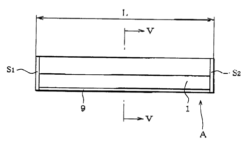
Meanwhile, n yumping light source for an optical-fiber
ampiifi~w having the structure sehematioally shown in N1g_
1 is known. The light source obtains an optical output of
250 mW or more from an optical tZber F by multipiAxi.ny
optical output:. supplied from two lasAr mod»1 Pc M dnd M
reopectively havstag an optical otrtpuL of approximately 1~0
mW by an optical coupler C_ The i~dque~st ror higher output
is intensigied to the liy~lL source.
~n rhA ra~A o~ the light source shown in Fig. I.
opr.iaal outputs suyylied rrom the laser modulc3 M and M ar~
dtt~muated when multiplexed by tho optical cvuplsr e.
Tlxererore. an optical output of a usable light source
becomes smaller than an optical output (sum of npr.ic:a1
Received Sep-t8-00 03:09am From-03 3d~9 T62d To-Smart d BI~Qar PaQa OOT
CA 02326723 2000-10-02
..~,fl(ltl (191?.J3 T11IJ 1 (; : fl7 rAX fl3 3459 75..~,4 ~~~~[~o~~~nPh l~
(lOJ3/05?,
3
outputs of two laser modules) which c:att be essentially
~xpected from laser mocW IPIS 17SPCj.. Tlir~L is. an energy
conversion erfici.anc:y which is deLined by the ratio of an
optical n»tptit- powwr. fraiu nn upticsl-fiber end to the total
driving power of laser modules a.s lowered, Moreover, the
fumc:~ion as a light source disappears if one of the two
nwdules M and M which are used in Fig.i fails, That is,
the light source is lacking in the reliability as a high-
output light source.
Moreover, ae a pumping light source in which opLic:ul
outputs from a plur8lsty of laser mo~lmlA~ are c:ouple~d, for
example, U_s_ patent No_ 5,936.763 discloses an art for
fabricating a hs~n-c~nrpmt ~ueupirig light source bY u9inq a
pi »r~l iry of semiconducacr larger modules having oscillation
1~3 wavele~yLhs diLLerent from each other, the oECillation
laser beams yr which are wavelength-multiplexed by a
wavelength-multiplexing voupler.
In this prior art. oCOillation laser b~ams from
3cmivonduotor laser d~vices in samicr~ndmtor laser modules
are fixed by a diti:raction grating ~nci then. wave~length-
multiplexed by a wavelqngrh-muitiplexiiic~ couplor.
However, ~nlhen ri xi.ng ( or locking ) an oscihatioa
aravelenc~th cp ~ semlco~s~luCat~r' laser device, it is difficult
~o sLxbly control an optical output booauEe the change in
dziving current and in embient temperature could cause th~
longitudinal modes of the oecillatsng laser light a! thA
semiconductor laoer to shift accorainr.Jly therPhy givtn~
rise to kinks in light output vArsus injection current
characteristics as shown in fig_ 2.
As a lager module far qo7viu~ such problems, the
folloafinc,~ semi ~c~n~lICaUL' ic~ser module is disclosed is U, E .
PatPDt Nn_ S,Sd~.030.
Received Sep-2B-00 03:09am From-D3 3d~9 T'J2d To-Smart i Blaaar Paae 008
CA 02326723 2000-10-02
:O(lO t191: f3 TI~IJ 1 ~ : t1~3 rAH 0;3 ;3459 75:4 ~~~0(~'~0~~~:~Ph l~
tlO9IO5:
4
That is, the moclmle disclosed in the U.~. Patent has ei,
structure ontellnP~1 by drrauy~ing optical fibers with a
grati ng forJnec~ Lhdrein at the output facet of a
~Aminanductur loser device. In this ease, a reflection
ba~izdwidth of the grating is act to a value larger than a
wavelength interval of longitudinal modes of a laser beam
oscillated from the semieonduotor laser device,
specifically to a value of a nm or more. so a~ tn miti.ge~Le
the Snflucnvc of the longitualnal-moQe fluctmtion vu au
optical output from an optical fiber of Lhe module when the
semiconductor laser aevicP is drivers.
The ahnva-~ASaribed grating shoWS a reflcvtion
spectn~m having a. wefiectance only in a wavelength range
about a specific wavelengrh ( 7v.o ) as shvwu im Fig . 3 . In
Fig. 3, the wavelength width he~twcdn the wavelength at
which the reflectance is hs1 f Ltie peals reflectance is
rAfB=red to r~~ rn~lcc:Lion bandwidth.
Howwvwr, when wavelength-multiplexing is performed by
LliG module o~ the prior art, the following problems occur.
z0 That is, as a result of potting the reflection
bandwidth of the grating to 2 nm or more, thA fipPCtral
width of a lager beam output from the opts rai fibr~r oL the
modulo incr~ases and thereby, the n»mher of oscillated
wav8leagths which can ha mulLipiexed by a Zr~InYClCngth~
multipleYin7 counlPr having a narrow transmission band
dRC:rPases. a..deyiee or multiplexing lowers, and the loss of
the waveldyLh-multiplexing coupler inoreaaes.
It is an object of the present invention to solve tha~
above-described problcmo of a semiconductor laser c7wvic:e
having a mufti-quantum well etz~uctura and to provirie n
scmiconduotor las~r device in which an opLic;t>ll output is
not lowered even it a cavity length is aeL Lo a value
larger than l0 0 0 dun .
Received Sep-28-DO 03:09am From-03 3459 lJ2d To-Smart i BIaQar Page 009
CA 02326723 2000-10-02
?,OO() O9/: ~3 T11IJ 1 ~ : ()J3 I' AH (l3 3459 75:4 ~P90(~'~o~~~~Ph l~! p
10/05:
Moreover, it is annthPr ~Ljoct of the present
invention to providA by using Che above-described
semieonduatar ldse~~ device a semiconductor laoor module in
arriich thA r3e~vice d~~iving currents can be devreaoed to
!~ pruvl~le~ high d~:iving reliability, and wavelength-
~«ulCiplexing coupler has o. small lose in wavelength-
multj.ple~cinQ. The semiconduotor laser module ox the
present invention van bo ueed as a high-output pnmpiny
light aourcc~ for an optical-fiber amplifier compared Lu e~
conventional pumping light sourae~ which has a maximum
optical-fiber output of 18o m~n1 or nwre, ror example.
DisGloaure of thn Invention
To achieve the aLvv~o-described objects, the present
18 iuventurs made intensive studicw and in the course og their
research, they noticed the fact that an optical output og a
semiconductor laser device is specified by an intAgrdLea
value of an cffivienay and an injected rnrrAnt density oL
the semiconductor laser d~vice and exruuined the relation
between efficiencies and aRVlty lengths og a semiconductor
las4r device having a lattices-uuiLchinQ-system quantum wall
structure .~nc7 a semiconductor laser device having a
lath nc~-misnmLulillg-system quantum well otructure with
respect to the noticed fact. 1~c a result, they has 2n idwa
that it is possible to fabricat~ a semiconductor laaRr
device for omitting light at a higtl ot~tpmt c:c~mpardd to a
conventional device by setting a vavi.ty lemgLh Lu a value
0qua1 to or more than a c:~artain value ~tnd then , further
continued the studies end finally developed a semiconductor
la:er device and a samic~o~~~luctor laser module using the
semi ~c~nducLUL' ltlSC.t device of the prcocnt invention.
TtiriL is, in the semiconductor la:.er device of tBe
present invention, a stacked Structure of a s~miconctucr.~z~
Rec~IV~d S~p-28-00 D3:09am From-03 3d59 T52d To-Smart 3 Blartar Page D10
CA 02326723 2000-10-02
000 O9/~ ~3 T1~LJ 1 ~ : 0~3 rAK O3 ;3459 75?4 ~P~pf~'~o~~~~Ph l~ 0111(15:
G
including an aotive layer comprising a s~trslne~d mui~i-
quantum well structure is formed on a s~.~h~tratP . a c;ewi Ly
length is larger than 1000 ~,.att but 1800 dun or less, a 1ow-
rerlzation film having a reflcotance of 3% or less is
3 formed on one (acct, and a high-reflection film having s~
reflectance of OO~r or more is form~d on the other fecat_
fartioularly, a semiconductoz~ laser devi ra amich has a
vomprecEed strained multi-quantum wPl1 struc;Luiw iu which
the strained mufti-quantum well strwcaure has a lattice-
mismatching rate of 0.5 to 1.5%, preferably 0.5 to 1.1% is
provid~d.
MU.L'-CSUVCZ', i;he present invention provides a
semic:omduci:or laser module in whioh a semiconductor yaser
device is sealed in a paokage whil~ set to a cooling aPVirw
compris~.nq Peltier clcmonts (thermoelectric effect
elements) and an optioal fiber a.s opposed to the ~mtput
(acct of the semiconductor laser d1'rvi c_e . Tlxe prGSent
invention provides a semiconductor. laaew module in which
the cooling G.evice 1~ prAferuLly constituted by
ZU electrically altArnstP7.y uLwanging 40 pairs or morc of p-
type rmd ii- Lypu conductive Pettier elemonto and holding
these elements by top and bottom vcramic substrates and in
which a grating having a rc~lcction bandwidth of 2 nm or
less, prefcrsbly 1.5 nm or less and larder t~.han the
longitudinal-mode wavelength interval nt a laser Ldam
oac111atAd from the semicondmatow laser device is formed on
the t'~.ber. 1n the suhswcpmnt dc~bc:riDtion , the number o~
pairs of a p-type amcl eon n-type Pettier elemcnto is defined
as "the number of fairs".
BRIEF DESCRIPTION OF TH8 DRAOPINGS
Fig. 1 is a schematic view showing a light source f~~~
pumping an optioai-fiber amplifier;
Recalved Sep-2H-0D 03:09am From-03 3d69 T~Jtd To-Smart i 6liQar Page Ott
CA 02326723 2000-10-02
i'.(Jfl(1 f1~31i'fi 'f'fl(J- l~('i:(lfi~ I~AK- (l;i~ ;i4!-n- 'l~:'.4'
~v~~a~'~'7~.'s~P~~ tø1f1-1?,I(1'~~'
7
Fig. 7 is a graph 5liuwing the light output versus
in~ACai on c:mrr.Pnt ctiawnc:l.eristic of a conventionEll
~,eau.iuu~Wuci:or laser module having art optival fiber with a
grrs L iilg ;
Fig. J is an illustration for explaining a reflection
bnndwidth of Nn optical fiber ooith a grating;
rig. 4 is a aide vices ~howing a samieonCUCtor las~r
dcvioc ~ of the present invention;
Fig. 5 is a cross-sectional vieta along tt~w line IV-IV
in ~~ig . j ;
~~ig. 6 is a schPmai-1 c view si~ow~.ng a semiconductor
1 asAr module Bl of Lhu present invention;
Fib. 7 is a schematic view showing another
sewi,c;uu~lucLvi laser module D, of the prcacnt inventioW
Fig. 8 is a. cross scotional view showring an optical
fiber tv be built in a module;
Fig. 9 is a graph shearing relations hRtwAAn cavity
longthE and maximum optical output pcwAr of a device of
Example and a device 1 of rcmpa=nLivd example:
Fig_ l0 is a graph ~howiu~ relations between cavity
7wngths and maximum optic:~sl output power of a device of
Example rued a device 2 of Comparativ~ example;
Fig. 11 is a graph showing the wavelength d~pendency
of the maximum optioal output of a semiconductor laser
device of the preoont inveati.on;
Fig. lZ is a graph showinr~ the rAla1-.ion belwrsdil the
number of pairs of yeltier elements used amt Lhe Pettier
porn~r consumption in a laser module:
Fi.g_ t~ is an i11u5Lration showing an electrical
3o conna~fiinn of PelLiei~ elements in a cooler used for a lacer
nmlule of Example 2 ; and
Fxg. 14 is a graph showing the relation between the
amount of heat generated at a semiconductor 1as~r aevicp
Racelved Sep-28-00 p3:08am From-D3 3dJ8 TJ2d To-Smart i BIQ~ar PaQ~ 012
CA 02326723 2000-10-02
?,Oflfl O9/?f3 TJ1IJ 1:09 1'AH (l;i ;3459 75?,4 ~P9~(~'~o~~~nph 1~01;3/tl5?,
s
and the power consumption of a c:oolew im a semiconductor
laser module fabricated. for Fxacnple 2.
BEST MODg FOR CARRYING 01JT THE INVHI~f1'ION
'S A cross-sectional structure of ono example of a
~dmiconductor laser device of the pre3ent invention is
shown in Fiq. 4 and Fig. 5 that is s vro~~-sectional view
along the line V-V in Fig. 4.
The device A has a structure in which a stac7ced
structure to be m~ntioned later is formed by performing
epitsxial growth of a predetermined awmiaonductox~ am a
substrat~ 1 maQe of rha prAdetercninad semiconductor by
ur~11-xnown epj.taxial growth mei:hods such as metal-organic
chemical vapor dsposlllucr meLlzod, liquid phase epitaxy
~uGlhod, molecular-beam epitaxy, qae sourve molecular-beam
epitaxy. or chemical-beam epitaxy, thon oleawage is
performed to get a prcdctormined cavity length (L), and
moreover a low rcflcvtion film Sl to be mention~d later i.s
form0d on one cl~aved raCet, a high-r.Prl Pscai on fiLn S~ i~
formed on the other cleaves facet, anc~ ft~rilmLUUure a lower
electrode 9 is formPC9 on the back of Lhe substrate 1 and an
upper electrodA R i~ formed on the upper face of the
s'i.sclcwd rtrucauiw.
The stacked structure shown in Fig. 4 has a buried
23 heterostructure (DII structure) in which a lower clad layer
2 made of, for example, a-InP, a lower grin-SCH layer 3
made of, for example, non-doped GaInASP. an activA layer 4
of a lattice-mismatehin'-system mufti-quantum well
structure mad~ of, for examples, GnzirAsP, and an upper Grin-
:i0 SCai layer 5 made of, for Axample, nun-doped QaInAsP are
sequr~ntinll.y r~tnc)ced vu Llle substrate 1 made of, for
Rxample. u-I11P. Mureuver. an upper clad layer 6 msdo of,
ror example, p-InP and a cap layer 7 made of, for example,
Received Sep-2~-00 03:~9am From-p3 3d38 T52d To-Smart 3 BIeQar Pace 013
CA 02326723 2000-10-02
flOO 09/?f3 T11f1 1 ~ : O9 rAH f13 ;1459 75:4 ~:~90[~:~'~a~~~~Ph l~J 014105:
9
p-GaInAS~ are stacked on the upper ~rtn-sCH laydw 5. Tlmc~.
an upper electrod~ 8 is formAC7 on the cap laydw 7 and a
lower electrode 9 1r formed um the back of the substrate 1.
fUrthPrm~rm, lny Stdokiy i11 order a p-InP layer 11 and
an u-InP ltsydi 12 on the side faces of the lower clad layer
Z, luwe~r Grin-SCFI layer 3, active layer 4, and upper Grin-
SCH layer 5, a current confinement; portion for supplying
current to the active layer 4 is formed.
In the above-described ntacJsed structure, the active
layer 4 is constituted of a strained multi-quantum well
structure. Specifica.Lly, a compressPn gr.rainwc~ multi-
quantum well structure 1 R ~PnrmPd iii wllioh a lattice-
mismatchin~ rate bernmw~ +~.5 Lu t1.5%. Dreferably 0.5 to
t.i~r to the substrate 1. Muweuvor, it is preferable that
LhG ~munber oL wells is 3 to 5.
When the absolute value of the lattive-mismatching
rate is smaller than 0.5%, the active layer 4 snows the
same behavior as the oaoo of a lattice-matciaing system_
For example, when a cavity length (L) is equal to 1000 Eun,
70 Lhd upLiLal output is 200 mW at most. When the lattice-
mismatchinq rate is larger than 1.5%, problems occur that a
crystal strain of the active layer is relaxed,
crystallinity is deteriorated, and laser device
charaet~ristics are deteriorated. P:~rtic:ulaL~ly, Llze larger
the number of wells ana the t~hir:kAr the wail-layer
thickness, thp more critical the problem is.
Moreover, iu Lhd uase or a semiconductor laser device
or the Hresent invention, by constituting the active layer
o~ the above-described lattice mismatching-Eyetem multi
quantum well structure and simultaneously setting the
reflectanoc of the low-reflection tilm Sj form~a on a
light-output faoet to 3% or lass as described later, it is
possible to realize high-output light rmi_yaiuu avdu when
Received Sep-28-00 03;09am From-03 3dR9 TDtd To-Smart 3 BI~Qar Paae 01d
CA 02326723 2000-10-02
:000 09/?f3 T11I1 1 ~: 09 rAH 0;3 ;3459 75:4 ~P90f~~o~F~~nPh ~I (715/05:
lU
1 nc:rAasing the cave Ly 1e5n5~th ( L ) to a Yalue larder than
1000 Eu~t. However, rarien settin7 the cave ty 1 Pngth (L) to a
value larger than 1800 Vim, deterioration of an optical
output due to internal absorption is rcvogniaed even if the
above-described requisite3 are met. Therefor~, the cavity
length (r.) i s spt- to a valud larger than 1000 ~,un but equal
to or lees than 1800 dun.
In thin cave, th~ retlectanc~ of the low-rAtlAntian
film Sl formed on the light-output facet is set to 3~ or
less and the reflectance nP the Hi~li-reLlection ii.im S,
gorm~d on the other f~nwt is sGL to 90a or more.
Par~.~cuir~.i:ly, it is necessary to set tho rcflcatanvc
of the low-reLlection film 3~ to 3% or lcsa. If the
reflectance is set to a value larger than 3%, the
efficiency is lowered and an optical output is aeteriorated.
It is preferable that the low-reelection film S1 is
aonotituted of, tot example, a siri~lP lRyPr of Also, or n
dielectric multilayer film obtained ni' altPrntctely
laminated Ai=~~ anQ 510, - MOreU V di , , to form the low-
:cu r~fl~ction teem S~, 1 t i S ~1USS1L1C to use the plasma CYD
me~t~od (PCVD method) or electronic cyclotron rooonance
sputtering method (ECR sputtering method). Among which the
ECR sputtering method io preferable because a high-
reliability low roflovtion film can be form~d_
Then, an oxample of the semiconauetor laser mo~lulA t
of the present invention shown in F10. 6 i~ described~below.
~1'he module Ftl has a stz~.~canre~ im which the laser
Qevice A of thw present invention already described is
sea:l.ed 1 n s~ pac:kagr_ 13 while it is net to a cooling devise
14 comprising a Dlurality of pairs of Poltior elements 14a
to be described later.
Recalved Sap-2B-00 03:09am From-03 3d39 T62d To-Smart i Blaaar PaQa 015
CA 02326723 2000-10-02
fltlO fl9/: f3 TJ1IJ 1 ~ : 09 rAK 0;3 3459 75:4 ~f~~p=. (i~~o~~~~ph l~101
(;/O5?,
m
A collimator 1~ns 15a ss set to the ltght~-omtPmt fanet
of the laser device A, an optical fiber 15 tc hA dPSarihAd
later is set to the front of the packaye 13 Llliuugll a
focusing lens 15b, and a nhotnr~iode 17 iS SdL i:o the back
of thR la~Ar. dcwice A.
Tn tt»: cnoaule H1. Llxe cooling device 14 is set in
ordei tv at~sorw lice heat produced during the operation of
the laser device A operates and thereby moderato the heat
saturation of the laser device A. This i~ realized by
monitoring the temperature of the semiconductor las~r
dcvioc A with a thermiEtor (temperature sensor) is fixecL in
the vieiriity of the semiconauCtar lacAr c~AVice A while
controlling a current to be supplied to Lhe Pellier element
14a 94 r.har. t.hw TPmpsrature indicated Ly Lhe Llminustor
hr~c:omAS c:onstam L .
Iu Lhie ca~sd, the larger the difference between the
tem,Derature of the environment r~herc th~ laser module H1 is
set and the temperature at ~rhieh the oemiconductor laser
dcvioc A i3 eonatantly controlled (the temperature
indieatod by the thermietor 1s), the lard~r a load app11wc3
to the cooling device 14 . As a rAfi» 7 r. , the poraer
consumption of th~ cooling dAVicP 14 increases and the
total power consumption ~f the whole laser module H1 also
inare~se~.
Tim power consumption of the coola.ng dcvivc 14 under a
certain operating condition wherein the amount of heat
produc~d by the semiconductor laser device A and
environmental temperature are definite) depends ~n the sine
of the Peltior element and the charaate.r.~.sti c.:~ thereof such
se magnitude of a see beck coefficient, b»t gPnetwlly it
becomes tar?er Gmen the n»mbHr of pairs used in cooling
d.~vice 1s smal.lPr r.han 40. ~~~1 the total power consumption
c~f Lhd uw~lule~ 81 also become large accordingly. Therefore,
Racn wd Sap-i9-00 03:09am Fram-03 3d69 T52d To-Smart 3 Blaaar Page ~1fi
CA 02326723 2000-10-02
;ooocr o~~;e- wn- ~'c-~ : o-~- mx- o.~ ;~4~~- v;~4~ ~~~~o~~~Ph- ~ cry ~rfco,~
12
it is preferable to set tile n»mhsr of paitn of PZltier
elements to be use.~L t0 4fj car more .
Tn thA above-d~~ca-ii~di3 structure, by increasing the
thicknASS or a bdee plaLd 13a made of Cu-W of a package to
which they cooling device 14 comprising the rclticr element
14a is fixed. the heat discharged to a heat pink (not
shovtrn) outside of the laser module through the bees plate
lea from the cooling dcvivo 14 ie sv dittus~d while passing
through the base plate 13a that it is possible to lower the
effective thermal impedance of the above-described hAat-
discharge path. Thereby, the load ~r thA cooling device 14
is msti~ated and Thp nno7l.ng effdct is improved. Therefore,
it is possi t31 A tc~ dwc:rea~te Llle~ power consumption of the
cooling device 14 aria SlaLly operate the laser module D,
also in a, higher-temperature environment.
I~ioovcver, ovhen extremely incrcaoing the thickness of
the base plate 13a, inereace of the thermal .Impedance due
to incrcaac of the length of a heat-discharge path becomes
more dominant than the reduction of a thArma7 i.mp~:danc;e due
30 to the above-described heat Gifrusinn and tlmtwLy, Lhe~
eoolinr~ effe~et by thw cooling device 14 dnc:reases rather.
T1: i ~ prA>'Arz~ble to sat the thickness of the base
p7atP 13d iii die upLimum range in such et trade-off relation.
Fig. 7 shooPS another semioonductor laEer module 8= of
2 5 the pres er~t invent ion .
The module 8, hue a structure in which a cooler 14A
oompricing plural pairs of peltier elements 14a and a
cooler 148 comprisin? plural pairs of Peltier elements 14b
are electrically arranged i n r~ packr~ge~ 13 in parallel .
jU In th~ case of thin ~truatuLw, the total power
c:onsumhtioic of Lhe mudulo under a curtain operating
CiUIlC~j.livm ( whe~re~iu 1:110 amount of heat produced by a
semiconductor lnaer device 14A, temperature of a thermistor
Received Sep-28-00 03:09am From-03 3d59 7R2d Ta-Smart d Bl ear PaQa 011
CA 02326723 2000-10-02
?,(l(1tl (19/: f3 T11IJ 1 ~ :1 (1 rAH f1;3 ;3459 75..~,4 ~~~Of~~o~F~a~:~Ph I~
01 ~3/O5?
13
18, and environm~ntal tempRraturc im which tha laser module
B= ss set ar~ definitR) 1~ almoeL dqual to the case of the
module B1 if the total iruruber of Pettier elements arc the
same. Rnt t-.hj.~ struc:Luiu has the advantages of lowering
the opdratiny voltage of a cooler, making it possible to
drive the cooler by a versatile inexpensive 5-volt power
supply.
In the case of the above-describQa module, it ss
preferable to use as an optical fiber 16 to be Duilt-in the
optioal fiber with a grating isb formed om a c:eW .iw1 core
16a thereof as shown in Fig . $ . Tn this c;ase~ , it is
preferabl8 that the rAfl.cacti~m bandwidth of the qro.ting 16b
is 2 nm or iPSR , partic:ula.r:ly 1 . ~ nm or less and larger
rrian the wav~lenytti lilLdrval of the longitudincl modoo of a
1!~ laser beam oscillated from the la3er device A.
The reason is described below.
First, ttm wdvelemyth interval (47v) of the
ton?ituQinal modA of a lnscr beam oaeillo.ted from the lacer
device A is shown by the following cquationi
30 e~ = 7~'/2n'I~
(wherein ~, denotes an oscillates wavelength, n dsnoi.eb Che
cfgectiwe refractive ind~x of the active layer a, and L
denotes a cavity length.)
Then, because thg cavity lAngLt~ (L) is longer than the
25 cavity length of the prior art ( 900 ~.tm) disolosad in r..hA
official gascttc of the above-describes U . S . ps~ r.wni: No .
5,485,030, Lhe wavelength interval (0~.) in the longitudinal
amdr~ is smaller than the cast of the prior art .
Therefore, in the case of this module, it is possible
30 to include more longitudinal modes in the retiqotion
bandwidth of the grating 7.6b formed on the opti c:al fi5~er 16
compared to the case of th~ prior art. In other wvr~Ia, it
Received Sep-28-OD 03:09am From-03 3d59 TH2d To-Smart 3 BIQQar Page 01H
CA 02326723 2000-10-02
:O()0 fl9I:~3 TllfJ IG:IO T!A~ 0;3 ;3459 75:4 ~:~~0[~'~0~~~:~Ph ~10191(l5?,
14
is pvcsible to mitigate the Kinxs in the light output
vcrvuo injection current characteristic of a laser bc~u
emitt~d from the optical fiber 16.
Moreover, in the case of this tnuaule, because the
wavclcngth intorval (~) in the longitunina~ mnc~A~ of a
laser beam oscillated of the semiconductor laser devl.ce p
is narrow, it is also possi.bl~ to sPt the reflection
bandwidth of a grating to a small va 1 »w of 2 tttu yr loan
without decreasing the number of ~nngitudinal modes present
lv in the retleotic~n b~n~7midth of the grating 16b, in other
worGs, ~hilP pravAnting Llw generation of k3_nks in the
11~HL uuLpuC Versus injection current vharaot~ri~tie.
Furthermore, in the case of thin modul~, by setting
the reflection bandwidth of the grating 16 to 1_5 nm or
less, particularly to 1 nm or less, a.t is possible to
completely dcoraaoe the ep~ctral 'vidth of a laser t~w~m
emitted from the optical fiber 16 _ Tttcrrrfure, it is
posexble to increase the aec~rpA of tnulLiplexing under
avavolenr~tn mu1 ti p1 Axing rsttd to decrease the loaa of a
2o wavelength-mnltiplPXitl~ ~uupler used.
Exrdtnple 1
1 ) Fabrication of semiconauar.nr 1 aser devic:e~
The burl~a heter_QCtrmature (BIi structure) shown in Fig.
l5 b was fabricated by rorming rt stacked structure on an n InP
s»bstrate 1 Ly use of the MOCYD method, the otructur~
ao~upwisimy a lower clad leycr 2 of n InP, a lower GRIN-scat
layer 3 of nvn-doped GaInAsF, an active layer 4 of a
compressed strained multi-quantum atell structure having
30 five quantum wc113 of a lattice-mismatching rate nt +n. s%
with barrier lay~r of (GalnLsP haul ng band gap ette~igy of
1. OaV, an upper G1i11N-SCFi layer 5 of non-dupdd GdInAsP , an
upper clan layer a or p-TnP, a~ud a caH layer 7 of p-GaInAcp,
Racolvad Sop-28-DO 03:U9am From-03 3dl59 T62d To-Smart i BIQQar Page 019
CA 02326723 2000-10-02
OOO (19/: ~i T11IJ 1 ~ :1 fl rAK t1:3 3459 75?4 ~P9~f~~o~F~~~Ph l~ O% ()/(l5:
is
and than forming a current confinement p~rr.i~n with a p-Tnp
laser 11 anrl an n-tnr layer 12.
Trien, the Example davicP shown im Fib. 4 was
fabricated by cleaving thA whole ~Lwuc;Lure Lo corm various
cavity leiig LZm ( L ) , forming a low-reflection film S1 having
x weflec:La.nc:d of 3~ on one cleaved face with AhO, by the
ECR sputi:e~ring method, and forming a high-reflection film
9s having a reflectance of 99% on the other oloaved face
also by the ECR sputtering method.
For oomparison, a d~vice was fabricated similarly to
the case of Example except that the active layer d has a
lattice-matching-system quantum wwll strucauiw wade of
GaIn.7~sP_ The Qevlce was designateri as Cuuipe3LraLive example
ffavi aP 1 .
1 s ( 2 ) Chrisacaeristics of device
Maximum optical outDUts of these two devices wcrc
measured while chanqinq cavity lengths (L). Fig. 9 shows
the measurement reaulta.
Ac 3.s apparent from Fig. 9, in the case of Comparative
example device l, not only the maximum optscal owtn»r. is
low as a whole but also it is oh~Arved that the maximuiu
optical output lowers dnA t~ internrsl absorption whop the
vavity length (L) becomes 800 arm or more. In the ease oP
Example device, however, lowering of the optical oufipuL due
to int~rnal absorption xs not oDservPd h~torr the c:aviLy
length (L) cxeeeds 1200 ~tm and moreover, tt~e ma3cimum
optical output of the device is appro~rimately :ilu mW and
thus, the a~vice performs high-output operations.
( 3 ) Influence of low-reflection fi l m S1
3o when the ~xamplP ciRVicw was fabricated. a low-
refiection ,t. j.l.m S= hewing a reflCC:Lance of 5~ was formed
whll R lcAwpi ng thw rPf'l.~:c:Lamc;c or the high-reflection film
S2 c~L 983 to rabricate a device different in cavity length
Recelv~d Sep-28-DO 03:09am From-03 3d59 T52d Ta-Smart i BIeQar Page Oz0
CA 02326723 2000-10-02
.~,~fl(1 (19/: ~3 T11L1 1 ~ :1 (l rAH 03 ;3459 75:4 ~P~~f~~o~F~~nph ~I fl: l
/(l5:
16
(L) . The lo~a-reflection film having ~ rPflPCtaIlG:C of 'rJ~
was desa.gnated as comparative examplA ~7sviee z. Im LhiS
case, the low-reflection fi 1.m Sl wus roi~ned by the PCVD
method_
Maxi.mtim c~tic:al uutputs of the above-described Examplo
clAVlc:r and Lhe Comparative example device 2 were measured
gUt' v~sriuu5 cavity lengths (L). The results arc Shown in
Fig. 10.
As is apparent from Fig. 10, even if the stacJced
atructurc i, the game ae that of J~:xample device. then the
rcfioetanoe of th~ law-reflection film Sl excRads~ ;%,
int~rnal absorption becomes 4cminant and l.hd maximum
optical output is Greatly lnwwr~:d.
m rha case of Example deviud having a cavity length
~.5 (L ) of 1300 Hun, a lots-reflection film ( A1=n, ) S1 h:~viy a
rcflootance of 3% was formed by the electron-hA~m (FB)
vacuum evaporation method and RCR spuLLdrillg method
respectively to perform an APC (Au.Lumatic Pvwe= Control)
rA1 1 at~i 1 1 i-.y tEas~t.
Whl.7.~: Llm camzye rate of an operating current after
operation for 1000 hours was 0.6~r in the cae~ of the former
method, it Was 0% in tha casc of tha latter method.
As is apparent from the above, it is~ necessary to sPt
the reflectanc~ of the tom-reglection r1 1 m Ss to 3% ur less .
25 In this eag6; it is found triat tbR 1 ow-reflec:Liuu .Ciltn S1
can b~ formed pratprabl.y by Lien ECR sputtering method.
~.~,ie
Research az~d development in a Raman amplifier ie
30 recently activ~ly performed in addition to an erbium-doped
optical-fiber amplifier. In Raman ampllriers, a pumping
light source hsviag a high output sn any waver~nGth nanc3 is
roquestod.
Received Sep-28-00 03:09am From-D3 3d59 T5ld To-Smart d BIaQar Pale 921
CA 02326723 2000-10-02
(lflfl f191: ~3 T11JJ 1 ~ :1 Q rAK (1;3 ;3459 75:4 ~~~~f~:'~o~~~nPh
X10.~,..~./(15?,
1~
ThAretore, a laser aevlce Tnr oscillaLiu~ wavelengths
of 1150 to 1550 nm by changing active-layew cuuyoaitions
was fabricated as the Ex~utyle advice. The cavity longth
(L) of the laEer device was set at 1100 E.~m and the facet
reflectance of it was set at 3~ on the low-r. Pf1 P~ti on ~1 ~~a
and at 98% on th~ high-ref lection side.
Fig. 11 shows the oscill ar.Ae-wavelength depeudettey cf
ttie maximum optical output cf the aLuve-Qdacribed laser
devie~. A maximum optical ~utpuL of 300 mW or more was
obtained a.t an oscillated wavelength of 1200 to 1550 nm~
HUWCVEjl., an optical output has a tendency of lowering a~
the oscillated wavelength bcoomoc ehorter. This is because
a heterobarrier that is sn onergy differ~nee netween an anP
cladding layer and an optical confinement layer aPCrPasA~
in a short-wavelength region and thereby, a non r~c~iative
current component going over the hetPrc~h~rrlAr heigliL
between p-InP cladQing layAr and upper optical confinement
lay~r increases.
MUL'~uVCt', increasing the thickness of a ~rcll l3yor in
2n .a c~uemLum well structuro is considered as an exemplary
method to further lengthening an oscillated wavelength. In
this exemplary method, howover, it is estimated that the
longer the wavclongth, the larger the strain energy
accumulated in an active layer Que to inareas~ im a~ well-
a5 layer ttaicKness , thus provicllng a fz~ctor fur r:ryatallinity-
Qet~eT.1 pr~ti cm _
A light-rE.'C:G'iVilly r~letnent in an oy~tical communication
System uses a light-receiving element made of GaInAe wh~.ch
has an absorption end in the vicinity of 1650 nm, beyond
30 which the light-receiving acnsitivity abruptly lowers.
Theroforc, approximately 1650 nm is a limit as a wave~Angt~~
of s signal light ~ourc~ at the long-wavel~ngth sidP_
Under such limitation, the pumping 1 1 ght :~ouwc:d fur a Raman
Racalved Sep-28-00 03:09am From-D3 3d59 T62d To-Smart i BI~Qar Paaa 022
CA 02326723 2000-10-02
.~,(100 09I: ~3 T11I1 1 ~ :11 TAB 0;3 3459 75~ 4 ~~~~[~o~~~~Ph t~ p, 3/05?
1a
amplifier necessary to ampliry the ~i~unl slzuuld be a high
optical output pumping light source nL approximately 1350
nm which is approximd.tely 100 nm shorter than 1650 nm.
ThRrAi~orA an optical semiconductor laser device of the
s pt'eseuL invention can Hrovide a high-output power i.n a
wave~le~ngth band betwoen 1200 and 1550 nm, and therefore it
can be preferably applied not only to a pumping light
source that oscillates in 1480 nm band for an orbiutn-doped
optical-fiber att>tplificr but also to a high-output light
source for a Raman amplitier_
Though the above-described Exsmrlw device uses a
t~ainhsP-based materiel, it is also possible to fabricate n
laser devlc.P in rh~ above-described wavelength band by
using a material such ~x~ GaImNAs or AlGaIn~rs .
Though the above-described Example devioe uses an n-
InP substrate, it is also possible to obtain the same
advantage by usling a p-InP substrate.
Ex~ l~ ~ 3
Laser modales Jil and 8~ shown 1 n Fi.g:~ . 6 cmd 7 were
ass~mblsci bx using thw l~xample device having a cavity
length (L) of 1200 Vim.
It 3houid be noted that the Example device i~ a
s~miconductor laser device opPratiny aL a.u upt:ical output
z5 from a racer of ZBO mW far. s ~3rivit~~ vulCaye oL 2.5 V arid a
ctri.vi ng c:mrrPnt of 1. 1 A. Therefore, the Exempla devivc
haE a heat gan~ration (G,,") o~ 1.1 (A) x o.s (v) -o.ze (~
0.3) W ~ 2.5W.
In thin aaEe, a Pettier element 14a accnr~ling to the
following specification was ur~~r7 to constitute the cvvliu~
device l4.
R~celved Sep-2~-00 03:09am From-03 3dJ9 TJ2d To-Smart i BIpQar Paso 023
CA 02326723 2000-10-02
.?,f)(10 fl9/: f3 Tln1 16:11 rAX O3 3459 75?.4 ~P9~('~o~~~:~Ph l~ (1?,4/()5?,
19
Shape: Rectangular-pars.lleid~ipcd bulk having
dimensions of 0.64 mm in lPnglfi, 0.64 mm in width, and 0.02
mm j.n height
Characteristics : Saebeck coeffici ant a~P 7_ _ o x lo-' VlK,
Derformancc index of 2.8 x 10''/K, recf.stivity of 1.1 ~c 1v 6
i~m, and heat conductivity o1' 1 _ 3 W/K/ut
A driving current (Tc). a Wiviny voltage (Vc), and a
power consumpTi on ( Wa ) of a c;~~ler were estimated when
driving the cooler while keeping the thermistor temperature
at a5°C, with the amount of hPat(p~) gmretw~e~rl at the
gxampl~ device of l . 5 Watts in an wnviroruueuLal i.W ttpe~rature
of 50"C for tho vacs of a cooler With d0 or 5o Peltigr
elements conncotcd a.n cerise in the laser module of B1
chows in Fig. 6 arid for the case of twn c:oo7.~:r:: c:cmmc;Ldd
in parallel, ~aeh eornprising Z5 pairs of serially connected
Peltiar elements, in thA laser mo~luZe of B2 shown in Fiq. 7.
The same st»c3y was performed for a cast of using a
cooler of the conveuticiml design having JO pairs of
PdiLier elements as Comparative example.
Table 1 shows the above result .
Recalved Sep-IB-00 03:09am From-03 3dJ9 T6ld To-Smart 3 BIQQar Pale Otd
CA 02326723 2000-10-02
?,00() O9L f3 TIlf1 1 ~ :11 rAH 03 ;3459 75?4 ~P9p=. (~~o~~~nPh ~I O:5If15.~.
zo
m
sa
a
1
~
d ~ U
~
1
.1
C
O
a
r N CV
x ~ x w w
~ b a~
a
V
I ' E I
n
a.. ~ p~I m M L' N
.~ "r cfi tw
~
~
N
4
m ..a
~ b
n
ri
.
C o '~~
y ~
~
.a
~,
w
eo
D
+~
y
C~
o '
m .a m rra
r- c~ N
O ~ '
. ~ N
W M . -~'
i
C4 u,
N O
m
tr'~m oo r- cc
ro'dI I
O r1
~ N
' a~ ,-, J~ t..
.-( t4
~ O i
l t
J p
N td
r
'a Wit' ~y cw,
~ H
w e
a
-.
N '
CW O p" M . cp Op
C I
~
O
U
M
.,
d
p G
O O C
o v
~
m
c c ca.
w ,I,., +
C ! O O
I a O _ ...,
.-, m +~ -.~ . '~a Oa
t
_ ~
U U a
I~
c~ u ~ ~ > vI~ c b ~ s
I
.. ~
O C
Cs .. p~ ._ U Df~ 4
~ ~
1.1 IIe~to
3 ' ' ' ~
P ~ O
m O '~O
n ra ~i ~ ~ ~
' a
. c o,. c~ r-~~-.I
Rocaivod Sap-28-00 03:OAam From-03 3d5H T52d Ta-Smart i Bl ear Pair 025
CA 02326723 2000-10-02
(lOfl O9/?,f3 T11IJ 1 G :11 rAH O3 3459 75?4 ~P~p=. Ii~'~a~~~~Ph lø1
Q?,6/(15?,
a1
The following are claritled from Fir.. 12 anQ Table 1.
(1) W'hon the number of pairs of reltier elementa is smaller
than 40, trie driving current and power. consump~iom of Lhe
cooling device sncrease in both 1 asAr modules Bl a~itl B, and
the total power cons~~imption of lh6 laser modules also
increases.
(2) on the other hand, w~ieu lim number of pairs o~ heltiar
ele.tueiiLS exueetla 40 , the driving voltage of the vooling
device rises but the Do~oer consumption of the cooling
device and the total power von~umption of modules decrease_
The power consumption is improved by 1 w or more for both
vases of 10 pairs and 50 pairs compared tn 1-.hA c:a~w of
using 30 pairs.
( 3 ) Whan thg number ox Na1 r.t er elements c:vttuec:ldd im berries
a.s increased, se.rlAS rwsi.ctauud increases. Therefore,
particularly, whwn :~ laser module is operated under N high
LeuyeraCure environment, a problem occur3 that voltage
~i.rvps at both ends of a cooler inerea3e and thereby, a
versatile inexpensive 5 volt power supply cannot be used.
ZO Therefore, by operating two coolers connected in parallel
ao shown in Table i and Fig. 7, each r_.oo7ar comprising 23 .
pairs of Pettier ~lements connecTed in series, Lhe power
cvnsusnption of the coolin3 QPVi c:A and elm total power
consumpzi.on cf the modules result in the same advantage ac
z5 Thp c:aRR af. opera~iu~ uiie cooler comprising 50 pairs of
Peltier.elemants. Moreover. al9o by using a cooler as
shown in Fig. 13 wherein each half of the Pettier etemQnts
in one cooler i3 electrically connected in series so thar_
p-type and n-type elements are alternate and wherein thesd
30 series arc electrically arranged in parallel, it is
possible to drive the cooler at a lUWCt' vulLago without
lowersng th~ cooline~ perrormanc:e of Lhe~ coating devise, and
Recalved Sap-t8-00 03:09am From-03 3d59 T~3Zd To-Smart 6 BIQaar Page OtB
CA 02326723 2000-10-02
?,(1(lO (191.~,f3 Tllll 1 ~ :11 >'AH f13 ;3459 75:4 ~~~~(~'o~F~~~Ph l~
(1:71(15:
2~
th~reforg to strive the rn~1 Ar by ~ vewsr~lile~ itxoxrromsive~ 5-
volt powRr s~upnlY-
Wtteu ~wu c:uuldrs aie used, Peltier elemonts may be
alec:l.wic:rilly awrry.tyed itz varallel in at least ono of the
coolers.
Then, a lesser module using a cooler oompri~ing 30
pairs of Pelticr elements which is Comparative example
(convcntiona,l cxampio) and a lacer module using a cooler
compri,ing 50 pairs of Pettier elements were fabricated.
Semiconductor laser devices useB for the above-de~scri.bed
laser modules are semiconductor laRpr c3AVl.aAS; respectively
having a vavity length of 1300 ~m stsown for J<sxamples 1, 2,
and 3. For thc~o laoer modules, power consumption of the
cooler when controlled so that the temperature indir..ar.ad by
13 the thermistor 18 is kept at 25"C at an environmental
tAmparar_ure of 65°C were examined by c:tratying amount or
hc3srt gAnwrai-.~tl at a semicutidur:Lor laser dev7~ce. The
rws;» 1 ts, ar. P s'huwm itt Fib . I4 .
As is apparent from fig. 14, in the osac of the layer
module using the cooler comprising 30 pairo of Pottier
clcmcnt3, it wa:. a.mpo~~ible to discharge t8e generated heat
in the region where the amount of heat generated at a
semiconductor laser device was 1 . y!, W or mor. ~a . On the
other hand, in the case of tbP 1 FiRPlT module usiu0 ltic
cooler eomprisinr~ 5o pairs of PPitiar cir_tudtxLs, thc~ yower
c:on.~uruptlot~ was kdpL lower than the case of the comparative
exruuplc in the region where the amount of heat generated
was 2 W or more. Moreover, the laser module had a
sufficient cooling performance even for an amount of heat
generated of 2.5 W and made it possible to cool a
oomioonduotor lacer device up to an amount of heat
generated of 3.9 W or more. ~t~herefor~, In order to cons a
Racelved Sap-28-DO 03:09am From-D3 3d59 T52d Ta-Smart Z BIQQar Page 02T
CA 02326723 2000-10-02
?OOO fl9L~,~,f3 T11I1 1 ~ :1: rAH 03 ;3459 75?4 ~~~p=. [3~~o~~~~Ph ~I fl:
~31f15:
23
semiconductor. lFl9Pr r7AV1 aP of Lim yresent invention is a
particularly high optical ouLpuL region, it is preferable
to use a uuuldr comyrising 40 pairs or more of rolticr
eletneii La siiuwn in this Example .
Ian this Example, Pettier clcmcntc respectively having
a length of 0 . 64 mm and a aridth of 0 _ 64 mm were used. ~t~he
sine of a Pettier element i3 dot restricted to such
dimcn3iona. That ic, in the case of a cooler comprising an
paa.r~ of Pettier elements, the total cross-sectional area
of Pettier elements contributing to heat disctiawyd ( i~z i.he
case of the present invention, the c~~uss-SdoLional area is
.rPtarrArl t~ as "heat-diaulmrye cross-sectional area" ) a.s
0_64 (mm) x 0.61 (mm) x 4U (pairs) x Z = 37._R mm'_
Therefore, it is clear that a coQlwr having a heat-
7.5 discharge cross-sectional area of ap~rL'uX.i~Ilr~Le~ly 30 mma or
more shows the advantage rai° thr pwe~eW : invention even if
j.t rcmpri sP5 less Litau 40 pairs of Pettier element9 .
Theta, Lwu upLical,-Tiber amplifier pumping light
sources each having the optical output of 250 mW from ~aeh
giber output cad are fabricated by using one laser module
H, of Example 3 and by using two laser modus~s each having
a oooler aompriEing Pettier elements and an optical-fiber
output of 110 mW shown in Fig_ 1 . Tab1 w 7 ~hovvs
operational specificatl~ns of LuLi~ light sources at an
environmcatal temperature of 5o°c and a-zh~rmistor
Lc~mperature of ZO°C respectively.
RiCl1 wd Sop-2A-00 08:OOam from-03 3dJ9 TJ2d To-Smart i BIQQar Page ~2E
CA 02326723 2000-10-02
:000 091: f3 T11I1 1 ~ :1 ? TAK 0;3 ;3459 75:4 ~~~~(~?~o~~~~Ph lø! fl?,9/05:
24
a
w x
o c
~ ~a
a a
cv n cV o0 00 O
X
Lf~ G~ M N n ~ M ~ y
~ -
M
o c.~ op m o
~ o
" t ocr c~
~ n
~
~
.r
~ p
tr7
a .~
~
,1
W fir
U
.a
v ~
yi ~C
J O
V
O ~7
r o " ,n c~ c~ ~-w n
~'
~ n c ~ c
o
m ~ c~ c.. N oo
+r w
Qr cV C~7 ~.r~ . - !-f O
'~
~ N r1 ~~ ~ l' M
cV r-~
C1 Lz . ~ La
m
Of ~ O 47
-~ O
4~ A1
rl Q1
y
~ a a
, '-_ r0
~ m V
_
4
Q v ~
~
'~ p C d
- .
_
-, ~ 3 ~ U o w .~-t
r
y
w m w r d .-. .,-~,~ y..r4.~
r.~
o ~ ~ ei a
N
.- w ~ o
-r
ru u, 0 ~ ~ a r_
~1 - $
C ~ O V
O
~ ~ O N '~~
' n LI
.~: Qrrnri b o C7 f-i
w ~ w
'
05 .~a c, co t.~o ,..~ v s
~ i ~
w
a c r r a --.a~cs._3a : o
~
~ V
b +~ L dl -I
V '
V m
~
a d ~ ~ ~ V m ~ ~ '.~ r
m r.
y b ~ H H . 3 ~~~ C IrN ~
yr '' z a .1 d
Em
iga a a b H ~ ~ w
w
0
cry o
Recelv~d Sep-28-00 03:OAam From-03 3d!!9 152d To-Smart 8 BI~Qar Paae 029
CA 02326723 2000-10-02
(lO() (19f: f3 T11t1 1 ~ :1: TaH 03 3459 75:4 ~P9pf~'o~F~~nPh l~J p3Q1f15?,
~5
Aa is apparent Lrom Table 2, the total power
consumption of system with the pumping light source
operated at more than required 250 mW of optioal output
from fiber output end i9 amallor for the oa~o with single
laser module of example 2 than for the conventional case.
Then, temperatures of activ~ layers of semiconductor
laEer deviceE of laser modules constituting the above-
descriDad optical-fiber-amplifier p»mpi nc~ 1 1 c~ht ~nt~rnP~
were compared and failure rates of both ~yst~ams ware
to ralGUl.ated whAn assuming that Llle~ above-described optical-
ribar-amplifier ptuupiuy 1ig11t sources had the same
activation energy (La) for wear-out failure of
semiconductor laser devices. The re3ult:. are shown in
Table 0.
The thermal impedance in Table 3 stsows the thermal
impedance bettyeen a 8em~.conductcr laser device and a
tharmiator when keeping the thcrmiotor temperature at 25°C.
In Example 2, the thermal impedanoc ohowo 12 (K/W) which ie
2/3 of the thermal impedance of Comparative example. ~rhis
i~ booau~~ the cavity length of a s~nticonductor laser
device of Example 2 is 1200 arm and thereby, the heat-
discharge area increaoes compared to the race of the
semiconductor laser device of Comparative example having a
cavity length of 800 Eun. In this case, the temperature
Tj(K~) or the active layer of the semiconductor laser devioe
is calculated by the following cxpreccion.
T~ (K) - ThArmi ~,ficm L~uydtdtuZ=a ( 25°C) t 273 (K) t
Thezmal imp~aanc~ (W/K) x Amount of heat generatPQ at la~wr
(W)
jU ~i~heregore, in the case of Example 2, Tj(K) is
calculates as follows.
Recta ved Ssp-18-DO 03:09am From-03 3d~J9 T52d To-Smart i BIQiar Page 030
CA 02326723 2000-10-02
()(1(1 09/.~,J3 T1IIJ 1 ~ :1 ? >! AX (13 ;3459 75..~,4 ~P9p=. (~o~F~~~Ph l~
031 /()5:
26
Tj(K) ~ 25 (~'C) + 273 (K) + 12 (K/W) x. 2_d5 (W) _ 327
(K)
In the case of Comparatsve example. T~(K) iR
ca.LCUlated similarly as ~olicaws.
T.1(K) ~ 25 (°C) + 273 (K) + 8 (K/W) x 1.45 (W) - 314
(K)
Whcn both vaoe~ are compared, it is found that th~
amount of hcat generated at ~.aser of Jrxample 2 is
approximately l.7 times larger thRn that of Comparative
eyample but temperatures of aativA layers of Exampia 2 and
CompRrt~ t 1 vA Axamp 1.e are aliuus t eQual to enah other .
Th~rwi'c~re! , it i~ pu5slLld to Drevent a temperature rise of
ale active layer by increasing the cavity length.
Moreover, a failure rate of a layer module ie shown by
the following expression.
Lascr module failure rate ( f.L'f ) = Laser wear-out
failure rate (FIT) + Laser ransom failure rate (FrT) +
failure rate of coupling-system (1~=T)
DdOreov~r, the toted rF1111trP rnLci of 1:11e CrDtiGal-fiber-
amrllfie3r. pumping light bounce is shoran by the following
wxpressivn.
TuLal railure rate (FIT) = Loser-module failure rate
(FIT) x (Number nP layer mudule~s to be constituted)
l5 Then~fore. as is anparr_W from Table 3, a pumping
llptii: ~ourc;e of hir~h-reliability is realised with the 250
~uTn1-yunping light source for optical fiber amplifier aE
configured in example 2 since the total failure rate
thereof is 1~60FIT, acing approximat~1y 50~ of that of the
pumping light Source wherein 2 of the ronvPnti.nnW laser
modul~ (140 mW) axe usad.
Rrcelv~d Sop-28-OD 03:OAam From-03 3dR9 T~J2d Ta-Smart i Bliaar PaQS 031
CA 02326723 2000-10-02
:000 091: ~3 T11I1 1 ~ :1: rAH 03 ;3459 75?,4 ~~~p~o~~~~Ph l~ 0;3:/05?
a~
Il 1D 11CC(Z1CSS Lu bay that the Dresent invention is
arlvantage3vus im Wc~ape3c L ur the total failure rata as the
number of laser modules to be constituted increases.
S T3bl,G
Pumping light romping light
source using source in Fic~.
Example 2 1 wing
nnnvPntinnal
la3cr module
(Comparative
_ example)
'J.'hertnal impedance ( 1 ;~ 1 8
K/W )
Amount of heat generatod 2. 4 5 1 . 4 5
at laser (W)
Active layer temperature 3 2 7 3 '~' 4
(Tj: K)
Activation energy (Ea . 0. 6 2 0. 6 2
dV)
T.aswr wwar-nut fallurA ~ 8 4 5 a
rate (FIT)
tia9Rr rsnclom tai lrira 2 8 4 ~ 8 4
ratty
(FIT)
Failure rate of ooupllnc~-1 4 0 0 1 ~ 0 0
system (FIT)
Laser-module failure rate I 9 6 8 1 7 F~ 7
( ~' 11' )
Total failure rate ( FIT 1 9 6 8 3 5 8 4
)
Mor~over. a cooler comprising 50 pairs of Peltier
elements was used for the laser module D1 9hoatn in Fig. 6,
sad driving conditions (driving ourrent of th~
ccmiconduotor lsoor davioe, temperature of the thermistor,
and driving current of the cooler) of the laser module sl
was set so that the amount of heat transmitted from the
lower portion of the cool~r to the base nl.ate 13a made nP
rn-TA rags 7A W. Tn this naFA, Ltie LrcupeswaL~lie~s at; 1:11e lower
faae of ttie brine plate 13a. LlinL is, the telriperatule of an
uaillustratod heat sink to vrhich the lager module Dl is
Racelv~d Sep-28-DO 93:09am From-03 3dJ9 TSZd To-Smart 3 BIQ~ar Page 03Z
CA 02326723 2000-10-02
(7(l0 09/: f3 TilI1 1 ~ : l: 1'AK 03 ;3459 75:4 ~~90f~o~f~~:nPh LøJ 03;3/5:
28
fix~d vas controlled to be kept at ZO°C. under the above-
described state, tcmpcratur~a of the lower dace ot~ the
cooler, that is, temperatures of the upper face of the »ase
plate 13a were meaeured for varsous thickness or the bass
plate 13a below the cooler_
As Comparative example, a besP p1 afiw hrwimg Lhe
thicxness of 1 mm of rhA ronventional struc:luie wc~s
measureQ simi, T art y _ The: resui L~ as:o shown in Table
Table 4
~Thiekncoo of baee Temperature of uppor geed of »ase
plato (mm) . plate ('C ) ('1'emp~aratuz'q o~ ~ oamr
face ie kept constant az iu°c:)
O. 1 5 ~. ~ 3
1 ~f1.22
Cornpazui.ivd c~xamDle
2 47.8
4 7. 1 6
5 4Ei.97
t 0 d ?. 5 5
7 i 4 ~3 , a '!
rrom Table 4, the fo3.lowing can be found. 'i~hat is, by
increasing the thivkneco of the base plate 13a starting
with 0.1 mm, the difference between the tAmpAreture of Lhe
upper face of and the Zemporature ~~ i:he luWC.L' facie
(constant at 20°C) of th~ base plate aocroases. However,
when the thivkncoo of the basB plate becomes 1u mm or mc~rP,
the temperature difference increas~s rather. The reason
why the temperature diff~rence be~twFPn the uppew eumi lvwe~r
ZO taCQS of the base plate showq R»c:h teiideuc:y c:at'i be3 thought
as f41.1_OW9 _ That 1 ~ , by imc:re~asing the thickness of the
Cu-W hasp p~ atA 1 3x. Lhe lxeat dischargod from the lower
Lace ur the cooler through the base plate 13a to a heat
Received Sep-28-DD 03:09am From-D3 3489 T52d To-Smart i BtQaar Paae 033
CA 02326723 2000-10-02
..~,(lOO 09/?,f3 T11IJ 1 G :1;3 rAH (l3 3459 75:4 ~~~p=. (~'o~~~~Ph ~I
034/05.~,~,
l9
sink (not shown) outside of the laser module diffuses while
passing through the base plate 13a and therefore, it is
possible to decrease the cffcvtivo thermal impedance of the
above dcsvribcd heat disvhargc path. However, by extremely
increasing the thickness of the base plate 13a, increase in
the thermal impedance due to increase in the length of the
heat-discharge path becomes dominant over the reduction
effect of the egfective thermal impAr7ann~a r7t~A tn ahnvA-
described heat diffusion. It is pr~ei~Prable that the
LlliClule~ss of Lhd Laws plate 13a is decided in an optimum
range in the trada~-orL relation. Specificnlly, it is
preferable to set the thickneae of base plate 13a in 3
rango of 3 to 10 mm. A laser module in which the thioknecc
of the base plate 13a i3 ociootod in the above-deEVribed
rang~ can be driven at a low power consumption because the
t~mp~rature dxt~terence between the upper and lower faces of
basR plate is small and ~ChAr~by, thA load on a cooler is
rRrlttc:Pt7 .
Example 4
Three types of semiconductor laser device9 having
cavity lengths (L) of 1000, 1300, and 1800 Nm and
s~ Lructures shown iii Flgs . 4 amyl 5 are rabrivated similarly
to the case of Example I. Moreover, the opticv.l fibers
shorn in Fig. 0 Here prepared in which gratings with
rcflcvtion bandwidth3 of l, 1.5, and 3 nm were formed.
Then, modules shown in Fig. 6 were fabricated by combining
them. Spectral widths of laser b~ams emitted from the
optical fibers were measur~d by arivinc~ these modmic~s.
Moreover, longitudinal-mode wsvclcngth intcrvalo (0~) of
the 3cmioonduvtor la3cr devioee and the number of
longitudinal modes preoent in reflection bandw3.dth of the
gratsngs worn ca~cu~ataa.
Racelved Sep-28-OD 03:09am From-03 3d69 T52d To-Smart b BIRaar PaQa 03d
CA 02326723 2000-10-02
QO(l 09I: ~3 T11I1 1 G :1;3 rAX O;3 ;3459 75:4 ~P~~[~;~~aq~~~:~Ph l~1
(135If15.~,~,
Tah1 P 5 c-c~1 1 c~caively sHc~wS both the measurement and
c:alcarlatian r.PSUlts. Reflcc;Lalie:es of the gratings used
wdLw rc~spectivaly set to 0~~ .
5 Table ~
Cavity lengtho~ laser
devic~ (h m)
,
1 0 1 3 0 1 8 0
0 0 U
0
Longitudinal-mode of
wavelength
interval
0. 1 0_ 0. I
5tuniounductorlaser device (~ nm ) 3 z 7
~ d
_
Number of Retlection of 3 2
bandwidth
- 4. 2 5. 8
lonyiluil,iiialra,tin 1 nm
modco preoent Reflection bandwidth of
,~. 8 6, z 8,
iu rerlection at 1.5 nm
_
band o~ R~f loction bandwidth of 6 ,~ g .e
~
, , I 1 1 .
wtzLing*I wuLiu 2 nm 6
Relevtion bandwidth of
Spectral I. U U. 8 U. b
i i'a Liu : 1 mn
th
of Rclcetion bandwidth of 1. ~ 1. U U. '/
d
w
light emitted
1 rarin _ 1 . ~ nm , .__
f
as~r Rcflovtion bandwidth of 1, g 1. ;, 1. 0
rom
module*2 (nm)
ra t 1 n n 7 ntn
*l: Defined by (R~t'1~etion oandvalnrh of grating:
iliti) / (hozvgi tL~di na 1 mndP int~xwal ur Set111COriduCtor laser
device : run )
10 *2: Wavelength Width where intcnoity of reflectance
spoctrum lowcra ~rom peak intensity dy lU d73
ThP light ~ntpnt vPr:,ua injection current
r..hara~r.Ariatic mPasuretu~mL done for any of semiconductor
13 laser modules corresponding to design psramctcr ahoWn in
Table r showed no kinks like in Fig. 2.
The following arc olarified from these results.
That i3, increacing the cavity ~.ength of the
semiconductor laser device to 1,000 hum or morn reduces the
Zo longituCinal-mode wav~lengtn i.ntRrval n~, cf r~ ~dmic;unductor
laser devices. thereby ms~king it possible to increase Lhe
Rec~IVed Sap-2S-00 03:09am Prom-03 3dJ9 T92d To-Smart i BIaQar Paaa 03J
CA 02326723 2000-10-02
(100 09/: ~i T11IJ 1 ~ :13 >' AX 0;3 ;3459 75:4 ~P9p=. (i'~'o~~~n~h I~
(13G/Q5?,
si
number oL longitudinal modes present in the reflection
bandwidth of a grating compared to the laser of
conventional number of longitudinal modes. Therefore, the
number of longitudinal modes present in the reflection
bandcaidth of the grating can be ~nough to prevent
generation of kinks in light output versus Injection
current characterietic$ even when the reelection bandwidth
or the grating is set to a small value t~f. 7 nm nr 1A~~_
Th~r~fore, is the present invention having a
14 semiconductor laser dC:ViUC W~lUSC Cavity length ranges
between 1000 and 1800 Eun anti a grating whose r~floetion
bandwidth is 1 run or less and larger than xhR iongixWinal-
mode wavAlBngth iritorval of the S~Pmi nnn~meat7r 1 ~se~r dcwi c:A,
r.hg ~ollcwing advant:a~es can be obtained: (1) the ligtil
autpuL ft'Ulll d ~J~LLL.I.I:UII(~IIC:Lur laser device is increased: and
n~u~wuve~ (2) generation of kinks in the light output versus
injection curreat characteristic is controlled because a
plurality of lonQitud3.ar~1 modes arc alwayo prowcrzt in the
reflection band of the gratings and (3) it is posssnle to
deoreaEe the spectral width of a laser beam emitted from an
optical fiber can be narrowed beo.ause the rAi'1 Ar.T1 cn
bandwidth of th~ gratincJ is 2 nm nr IASS_
The.rato7~R, a r..n»pllng leis whemuulLipldxing laser
Lr~arns rrom semiconductor laser modules by use of a
wavelength-muZti.D~.eaing couplers can be lowered, thus is
provided a semiconductor laser module oapable of augmenting
a degree of multiplcx~.ng and therefore suitable for
obtaining higher output by wavelength-multiplexing_
Moreover, as is apparent from Table 5, even when the
:iU reflection bandwidth of a grating is set to 1.5 nm or. la9R,
the number o! lonc~it~idinal modA~, euougti Lu piwvcmL
g~enRrari~n of kinks in the liyhL uuL~ruL ve3ir~u~c iiYjeCtion
uurre~nt characteristic is Dresant in the reflection
Rec.lved Sep-28-00 03:09am From-03 3d59 TJ2d To-Smart i BIQQar PaQ~ 03fi
CA 02326723 2000-10-02
:OQO fl9/: f3 T1IIJ 1 (u :1;3 rAH 0;3 3459 75:4 ~~~0(~;~'~o~~~~Ph ~I O371(15:
3a
hs~ndwi e3th ni' a grating and Lhe~iwLy, it is possibl~ to
grAat 1 y drarsase the spec: Li-~al width of the light emitted
Lrom a semiconductor laser module while preventing
generation of thz kinks. Particularly. when setting the
reflection bandwidth of a grating to 1.5 nm or lesE and the
Cavity l.r3r7~c3'th ~i° ~ ~Ami aonducLui la~e1' device t0 1300 Eun or
more or rahen setting the cavity length to lUOU Eun or more
and the rofleotion bandwidth of the grating to 1 nm or less,
it iE possible to greatly decrease the spectral Width of
the light emitted from an optiCtil fihAr to 1.0 nm or less
xn any case. Th~refore. it iR possible Lu fe~bricaLd a
rwmi.aonduetor laaei- uwdule which is further prefernblc to
obLe.:iii a 111~jZltlL' uuLpui: by wavel~ngth multiplexin~l.
Iadustrial llpplioability
The semiconductor laser device o~ the present
3.nvcntion hardly caueee deterioration in an output due to
internal absorption. Therefore, it can be driven aT a high
output and thus it is useful ~~ a high-output light source
1U for optical-finer amnl.i t1 ~ati on .
Mo~duvdr, with the semiconductor module of the prc~ent
invention tabr3.cated by using the semiconduotor layer
device, the total power voncumption for driving can be
small and the failure rate of a systam in whseh the laser
module is built can be halved eompareci.to The Cnnvpntiondl
system failure rate, so the reliab111ty 1~ improved.
Furthermore, because cg r~ higlx optical output obtained
from a 1 asAr mocinlA of i:hP presdnt invention, ~.t is
possible to substitute siu~lC module for a plurality of
la$c~r modules used being wavelcnqth-multiplexed or
Dolarization-multiplexed. Therefore, with a la3cr module
of the present invention, it is possible to ~teareaso the
Racslvad Sep-tB-DD 03:09am From-03 3d69 T~2d To-Smart i Bi~~ar Pale 03T
CA 02326723 2000-10-02
.~,Of)(l (79L~.f3 T11f1 16:13 rAH O:3 3459 75:4 ~~~Of~o~~~:~Ph 1~p3~3IO5:
33
number of optical parts used >~or an opTi ~a1 -P1 hPr ~.mplifi~r
and realize a low-cost and compact numpi ng .7.i.ght sou~-c:e.
Moreover, by using an optical fivdr in which a grating
having a reflection handwir7th of 2 um ut less. particularly
7. . !5 nm nr 1 A~~ when Lhe uwdule is Fabricated, it is
pnc~i hl A tn circa~eaaa Lhc spectral atidth of s laser beam
emitted fawn the o~7 t,ical Tiber . Thus can be provided a
puiqpin3 light source having a small loco rahon wavelengtY~-
multiplexed by use of a wavelength-multiplexing coupler
with a narrow transmio::ion band and thereby having a higher
optical output oompar~d to a conventional light source.
Thus, 3cco=cling to the pre9Pnt invantiou, LL is~
porsible to provide a compact, inwx~~enaiv~, bul: liigh-output
optical-tihAr amplifier when cousllluLiu~ an u~rtical-fiber
amps 1 t'1 wr ~uah ns~ au rr.cbium-doped optical-fiber >:unplifier
or Rxmdn ~uplifirit .
Received Sep-28-00 03:09am From-03 3d5A 7'32d To-Smart b BIaQar Page 038
CA 02326723 2000-10-02