Note: Descriptions are shown in the official language in which they were submitted.
CA 02326873 2000-11-24
- 1 -
TITLE OF THE INVENTION
APPARATUS FOR RECEIVING TONE SIGNAL, APPARATUS FOR
TRANSMITTING TONE SIGNAL, AND APPARATUS FOR
TRANSMITTING OR RECEIVING TONE SIGNAL
BACKGROUND OF THE INVENTION
The present invention relates to a tone signal
receiving apparatus for detecting a tone signal, a tone
signal transmitting apparatus for generating a tone
signal, and a tone signal transmitting/receiving
apparatus having a function of receiving a tone signal
and transmitting a tone signal, which are used in
the field of communications and, more particularly,
to a tone signal receiving apparatus, tone
signal transmitting apparatus, and tone signal
transmitting/receiving apparatus, which implement
the above tone signal receiving apparatus, tone
signal transmitting apparatus, and tone signal
transmitting/receiving apparatus by digital circuits,
respectively.
Conventionally, in a key telephone system used in
an office building or business office, a key telephone
main apparatus (to be referred to as a main apparatus
hereinafter) having a switching function has the
arrangement shown in FIG. 1. Reference numeral lA
denotes a main apparatus.
Referring to FIG. 1, the main apparatus lA
comprises a trunk unit 11, line card 12, time switch
CA 02326873 2000-11-24
- 2 -
section (to be referred to as a TSW hereinafter) 13,
control section 14, and DTMF (Dual Tone Multi
Frequency) signal receiving section 15. These
components are connected to each other through a voice
bus (to be referred to as a PCMHW hereinafter) 16 and
control bus (to be referred to as a DHW hereinafter) 17.
The trunk unit 11 is connected to an external
communication network NW through a subscriber's line
ISL and has an interface function to the external
communication network NW. The line card 12 is
connected to extension terminals T1 to Tm through a
plurality of extension lines EL1 to ELm and has an
interface function to these extension terminals T1 to
Tm. Examples of the extension terminals T1 to Tm are
standard telephone sets and key telephone sets.
The TSW 13 selectively connects the trunk unit 11
to the line card 12 in accordance with an instruction
from the control section 14. The TSW 13 also
selectively connects one of the trunk unit 11 and line
card 12 to the DTMF signal receiving section 15.
The DTMF signal receiving section 15 has a codec
15a and PB receiver 15b. The codec 15a converts an
input digital signal into an analog signal and outputs
the analog signal to the PB receiver 15b. The PB
receiver 15b detects and identifies a DTMF signal from
the input analog signal.
The operation of detecting a DTMF signal in the
CA 02326873 2000-11-24
- 3 -
main apparatus lA will be described below.
When the user presses a dial key on the extension
terminal T1, a DTMF signal according to the dial key is
generated from the extension terminal T1. This DTMF
signal contains high- and low-frequency orthogonal
components, as shown in FIG. 2. The DTMF signal is
transferred to the TSW 13 through the line card 12 and
PCMHW 16 and then transferred to the DTMF signal
receiving section 15 through the TSW 13 and PCMHW 16.
In the DTMF signal receiving section 15, a number
of codecs 15a must be prepared in units of channels
because each codec 15a extracts a signal on a
predetermined channel of a number of channels
multiplexed on the PCMHW 16. The necessary number of
codecs 15a is eight for 100 accommodated lines. Hence,
the DTMF signal receiving section 15 has a large
circuit scale, and integration for cost reduction is
difficult.
In recent years, processing by the DTMF signal
receiving section 15 may be implemented using a DSP
(Digital Signal Processor).
FIG. 3 shows the internal block of a DTMF signal
receiving section using a DSP.
This DTMF signal receiving section comprises a
control bus interface section (to be referred to as a
DHW I/F hereinafter) 21, CPU 22, and DSP 23. The DHW
I/F 21 has an interface function to the DHW 17. The
. . CA 02326873 2000-11-24
- 4 -
CPU 22 controls processing of the DSP 23 on the basis
of a control signal supplied from the DHW 17 through
the DHW I/F 21. The DSP 23 has a storage section 231
which stores a Goertzel algorithm to be described below.
More specifically, the DSP 23 detects and identifies a
DTMF signal from a PCM signal supplied from the PCMHW
16 in accordance with the program stored in the storage
section 231 upon receiving an instruction from the
CPU 22.
The Goertzel algorithm will be described below.
This Goertzel algorithm is optimum to DTMF signal
detection by the discrete Fourier transform, in which a
signal on the time axis is converted into a signal on
the frequency axis and output, as in the Fourier
transform. Generally, in the Fourier transform, when
input signals at N sampling points on the time axis are
calculated, output signals at N points are obtained on
the frequency axis. In the Fourier transform, however,
when only eight frequencies suffice as output points
for such DTMF signal detection, the arithmetic
operation is wasteful.
To prevent this, in the Goertzel algorithm, the
number of samples is selected such that a spectrum only
at a specific frequency is output, and the square of an
output value is calculated to eliminate the complex
number generated by the arithmetic operation so that
only a real number can be output to make the processing
. CA 02326873 2000-11-24
- 5 -
easy. Note that the DTMF signal is a mixed wave of one
frequency selected from four low-frequency components
and one frequency selected from four high-frequency
components, as shown in FIG. 2, and is represented by a
mixed wave in a total of 16 combinations. Hence, when
the DTMF signal is Fourier-transformed into a signal on
the frequency axis, each of the two, high- and
low-frequency components contained in the DTMF signal
is represented by a peak value at one point. The DSP
23 can recognize and detect the type of DTMF signal
from the combination of two frequencies corresponding
to the peaks.
However, for the above-described method using the
DSP 23, a program for executing the Goertzel algorithm
must be created. In addition, causing the CPU 22 and
DSP 23 to execute the Goertzel algorithm requires to
prepare a number of ROMs or RAMs or a large-capacity
memory in the DSP 23 and also requires to change the
CPU 22 to a processor compatible to high-speed
operation. These pose a serous problem in integration
and cost reduction of the DTMF signal receiving section
and also increase the power consumption.
FIG. 4 shows the arrangement of another
conventional key telephone system. In this key
telephone system, a main apparatus 1B has a tone signal
generator 18. The same reference numerals as in FIG. 1
denote the same parts in FIG. 4, and a detailed
CA 02326873 2000-11-24
- 6 -
description thereof will be omitted.
The tone signal generator 18 is connected to a TSW
13 and control section 14 and time-divisionally
generates a tone signal formed from a plurality of
kinds of waveforms in accordance with an instruction
from the control section 14. The tone signal is
selectively sent to extension terminals T1 to Tm by the
TSW 13.
To time-divisionally generate a tone signal, the
tone signal generator 18 stores data in a ROM 181, as
shown in FIG. 5, and extracts data therefrom.
The ROM 181 has continuous areas for storing data
of waveforms #1 to #n-1. The areas have the same size
of m bytes. Each area stores the amplitude value data
of the waveform to be generated. One waveform is
generated by reading the m-byte data in accordance with
the order from #1 to #n-1.
The tone signal generator 18 also has a counter
182 for waveform number switching and a counter 183 for
data number switching. More specifically, in the tone
signal generator 18, data represented by an address
value obtained by adding, by an adder 184, an upper bit
output from the counter 182 and a lower bit output from
the counter 183 is extracted from the ROM 181 and
output.
The operation in the tone signal generator 18 will
be described. The counter 182 counts from 0. When the
_ CA 02326873 2000-11-24
count value reaches n-1, it returns to 0, and
simultaneously, the value of the counter 183 is
incremented by one. The counter 183 also counts from 0,
and when the count value reaches m-1, it returns to 0.
The adder 184 adds the output value from the counter
182 as an upper bit and the output value from the
counter 183 as a lower bit to generate an address value
and gives it to the ROM 181. When such operation is
continued, the waveform data are output from the ROM
181 one by one whereby n waveforms are time-
divisionally output.
However, since the waveform data are stored in the
ROM 181, the circuitry of the tone signal generator 18
becomes bulky, resulting in difficulty in integration.
In addition, since predetermined waveform data are
stored in the ROM 181, the tone signal generator 18
cannot flexibly cope with a change in frequency and
amplitude of a waveform, a change in data compression
scheme, and switching between 2-frequency addition and
2-frequency alternating in an output waveform. To
solve these problems, the tone signal generator 18 must
be inevitably modified in design of the ROM 181,
resulting in an increase in cost.
BRIEF SUMMARY OF THE INVENTION
It is an object of the present invention to
provide a tone signal receiving apparatus, tone signal
transmitting apparatus, and tone signal
CA 02326873 2000-11-24
_ g _
transmitting/receiving apparatus which can realize
downsizing and reduction in cost and power consumption
by integration using a simple digital circuit.
More specifically, it is the first object of the
present invention to provide a tone signal receiving
apparatus capable of suppressing an increase in circuit
scale, reducing the cost, and forming a one-chip
structure in realizing tone signal discrimination
processing by a digital circuit.
It is the second object of the present invention
to provide a tone signal transmitting apparatus capable
of reducing the memory capacity and also flexibly
coping with a change in frequency and amplitude of a
waveform, a change in data compression scheme, and
switching between 2-frequency addition and 2-frequency
alternating in an output waveform.
It is the third object of the present invention to
provide a tone signal transmitting/receiving apparatus
capable of realizing tone signal transmission and
reception processing by a single apparatus while
minimizing an increase in circuit scale.
The tone signal receiving apparatus according to
the present invention is directed to a tone signal
receiving apparatus for executing reception processing
of a tone signal generated by arbitrarily combining a
plurality of reference frequencies.
In order to achieve the above objects, the
CA 02326873 2000-11-24
_ g _
apparatus comprises arithmetic processing means for
adding a predetermined first reference value for each
of the plurality of reference frequencies and a
predetermined second reference value for each of the
plurality of reference frequencies to calculate an
arithmetic value at current time for each of the
plurality of reference frequencies, the first reference
value being calculated by multiplying the arithmetic
value for each of the reference frequencies by a
coefficient, which is held in said processing means,
before a predetermined period which is n times of
sampling periods, wherein n is an arbitrary natural
number, the coefficient being determined in accordance
with each of the reference frequencies, the second
reference value being calculated by subtracting the
arithmetic value for each of the reference frequencies
from a current tone signal, which is held in said
processing means, before 2 times of the predetermined
periods, and the arithmetic value being obtained by
repeating processing of adding the first reference
value and the second reference value a number of times
equal to a number of samples corresponding to each of
the plurality of reference frequencies.
The apparatus also comprises output value
extraction means for extracting an output value equal
to or larger than a predetermined threshold value from
the product-sum arithmetic values for the respective
. . CA 02326873 2000-11-24 ._
- 10 -
reference frequencies, which are calculated by the
arithmetic processing means, and signal determination
means for determining a type of the tone signal on the
basis of at least two output values extracted by the
output value extraction means.
The processing means comprises subtracting means
for subtracting a signal the 2n sampling periods before
from the tone signal, adding means for adding an output
from the subtracting means to signal before the
determined period to output the arithmetic value, first
delaying means for delaying an output from the addition
means by the determined period, second delay means for
delaying an output from the first delay means by the
determined periods and outputting the value to the
subtracting means, and multiplication means for
multiplying the output from the first delay means by
the coefficient corresponding to the reference
frequency and outputting the value to the addition
means, and also comprises a memory circuit which stores
a number of samples and coefficient corresponding to
each of the plurality of reference frequencies, and
arithmetic control means for sequentially reading out
and outputting each number of samples and coefficient
from the memory circuit every time arithmetic operation
for one reference frequency is ended, and giving the
coefficient to the multiplication means to execute
arithmetic processing a number of times equal to the
CA 02326873 2000-11-24
- 11 -
number of samples.
According to this arrangement, a product-sum
arithmetic device which constructs the Goertzel
algorithm by a digital circuit is used to discriminate
a tone signal. This product-sum arithmetic device has
a feedback loop structure in which the first reference
value for each of the plurality of reference
frequencies of the tone signal before the determined
period and the second reference value for each of the
plurality of reference frequencies of the tone signal
before 2 times is the determined period are added to
calculate product-sum arithmetic values at the current
time for each of the reference frequencies a number of
times equal to the number of samples for each of the
reference frequencies. When appropriate numbers of
samples and coefficients corresponding to all reference
frequencies possibly contained in the tone signal are
ensured, the apparatus can cope with an arbitrary
frequency contained in an actual tone signal without
requiring any extra dedicated circuit. When at least
two output values equal to or larger than the
predetermined threshold value are extracted for the
product-sum arithmetic values obtained by the
product-sum arithmetic device, a frequency contained in
the tone signal can be detected, and the type of tone
signal can be determined on the basis of the detection
result. That is, tone signal detection processing is
_ , CA 02326873 2000-11-24
- 12 -
divisionally executed by the respective digital
circuits so that DTMF signal detection processing
equivalent to the conventional processing using a codec
section and processing using a DSP can be realized.
For this reason, when the product-sum arithmetic
device having the Goertzel algorithm constructed by a
digital circuit is used, creation of a program for
executing the Goertzel algorithm and a large-capacity
memory for storing the program are unnecessary. In
addition, when the tone signal detection processing is
divisionally executed by the respective digital
circuits, the process capacity of one digital circuit
can be lower. Hence, an increase in circuit scale can
be suppressed, allowing integration and cost reduction.
According to the present invention, there is also
provided a tone signal transmitting apparatus for
time-divisionally generating a tone signal formed from
a plurality of types of waveforms, comprising amplitude
information generation means, having a memory whose
information contents are rewritable by an external
control signal, for sequentially outputting a plurality
of types of amplitude information written in the memory,
frequency information generation means, having a memory
whose information contents are rewritable by an
external control signal, for sequentially outputting a
plurality of types of frequency information written in
the memory, sine wave generation means for outputting a
CA 02326873 2000-11-24 ..
- 13 -
sine wave signal as the tone signal on the basis of
amplitude information and frequency information output
by the amplitude information generation means and the
frequency information generation means, and reset means
for resetting the sine wave generation means at a
predetermined interval to stabilize the sine wave
signal output for the sine wave generation means.
According to this arrangement, instead of having a
memory storing waveform information, the memory which
store the amplitude information and the memory which
store the frequency information, are used, when the
plurality of types of amplitude information and the
plurality of types of frequency information stored in
these memories are sequentially read out, a sine wave
signal to be sent as a tone signal is generated. For
this reason, the memory used in the entire apparatus
can be made small. In addition, the waveform to be
generated can easily be changed by rewriting the
frequency information and amplitude information in the
memories on the basis of an external control signal.
In generating a waveform, the waveform changes due to a
calculation error. However, the sine wave output can
be stabilized by resetting the sine wave generation
means at a predetermined interval.
In the above arrangement, the reset means resets
the sine wave generation means when the sign of the
sine wave signal output from the sine wave generation
. CA 02326873 2000-11-24
- 14 -
means changes from + to - after the elapse of a
predetermined period.
According to this arrangement, instead of
resetting the sine wave generation means immediately
after the elapse of the predetermined period, it is
reset after the waveform changes from + to -. Hence,
the sine wave generation means can be smoothly reset
without interrupting the output waveform.
In the above arrangement, the apparatus further
comprises rectangular processing means for selectively
deriving the sine wave signal output from the sine wave
generation means or the amplitude information output
from the amplitude information generation means using
an output selector for switching in accordance with an
external control signal so as to selectively replace an
amplitude value of the sine wave signal output from the
sine wave generation means with a fixed value.
This arrangement enables control to determine
whether the sine wave signal is to be converted into a
rectangular wave signal by external control. When a
sine wave can be generated using an amplitude value
after rectangular processing by selectively replacing
the amplitude value of the sine wave signal output from
the sine wave generation means the fixed value by the
output selector, the amplitude value information
storage device for rectangular processing can be
omitted.
CA 02326873 2000-11-24
- 15 -
In the above arrangement, the apparatus further
comprises addition/alternating processing means, the
addition/alternating processing means comprising an
adder for adding the sine wave signal output from the
sine wave generation means and an output from the
rectangular processing means, an alternating processor
for alternately selectively outputting an output from
the sine wave generation means and an output from the
rectangular processing means at a predetermined period,
and an output selector for selectively deriving an
output from the adder and an output from the
alternating processor on the basis of an external
control signal.
According to this arrangement, with the output
selector for selectively deriving the output from the
adder or the output from the alternating processor on
the basis of an external control signal, addition
processing and alternating processing can easily be
switched in accordance with the tone signal to be
generated.
In the above arrangement, the apparatus further
comprises compression means, capable of switching
between a first compression rule and a second
compression rule for different compression schemes on
the basis of an external control signal, for
selectively compressing an output from the
addition/alternating processing means on the basis of
CA 02326873 2000-11-24 ..
- 16 -
the first compression rule or the second compression
rule.
According to this arrangement, the compression
scheme for the tone signal to be generated can be
changed anytime in accordance with an external
instruction.
According to the present invention, there is also
provided a tone signal transmitting/receiving apparatus
for receiving and processing a tone signal formed by
arbitrarily combining a plurality of reference
frequencies within a predetermined band and generating
and transmitting a tone signal having a desired
frequency, comprising addition means for adding a
predetermined first reference value for each of the
plurality of reference frequencies and a predetermined
second reference value for each of the plurality of
reference frequencies within the band of the tone
signal to calculate a product-sum arithmetic value at
current time for each of the plurality of reference
frequencies, first delay means for delaying an output
value from the addition means by n (n is an arbitrary
natural number) sampling periods, second delay means
for delaying an output value from the first delay means
by the n sampling periods, multiplication means for
multiplying the output from the first delay means by a
coefficient determined in accordance with a reference
frequency to calculate the first reference value for
CA 02326873 2000-11-24
- 17 -
each of the reference frequencies, and subtraction
means for calculating the second reference value from
an output value from the second delay means, wherein in
a tone signal transmission processing mode, the output
value from the second delay means is set to an initial
amplitude value determined in accordance with a
frequency of a tone signal to be generated, a
coefficient determined in accordance with the frequency
of the tone signal to be generated is given to the
multiplication means, and the second reference value is
generated by the subtraction means by inverting the
output value from the second delay means, and in a tone
signal reception processing mode, an input signal is
input to the subtraction means, the product-sum
arithmetic value for each of the reference frequencies
the 2n sampling periods before is subtracted from the
input signal to calculate the second reference value
for each of the reference frequencies, and the
coefficient determined in accordance with the reference
frequency is given to the multiplication means.
In this arrangement, in the tone signal
transmission processing mode, the first reference value
obtained by multiplying the product-sum arithmetic
value the n sampling periods before by the coefficient
determined in accordance with the frequency of the
desired tone signal and the second reference value
obtained by inverting the product-sum arithmetic value
. CA 02326873 2000-11-24
- 18 -
the 2n sampling periods before are added to obtain the
tone signal to be transmitted. In the tone signal
reception processing mode, product-sum arithmetic
processing of adding the first reference value obtained
for each of the reference frequencies by multiplying
the product-sum arithmetic value for each of the
reference frequencies the n sampling periods before by
the coefficient determined in accordance with the
reference frequency and the second reference value
obtained for each of the reference frequencies by
subtracting the product-sum arithmetic value for each
of the reference frequencies the 2n sampling periods
before from the current input signal is repeatedly
executed for the respective reference frequencies.
That is, the product-sum arithmetic device which
constructs the Goertzel algorithm by a digital circuit
is shared by tone signal transmission processing and
tone signal reception processing. In accordance with
the tone signal transmission processing mode or tone
signal reception processing mode, the coefficient and
parameter values are selectively given to the
subtractor, multiplier, and second delay element in the
product-sum arithmetic device.
Hence, according to the above arrangement, the
product-sum arithmetic device need not be separately
prepared for tone signal transmission processing and
tone signal reception processing. In addition, in the
CA 02326873 2000-11-24
- 19 -
tone signal transmission processing mode, a tone signal
having a desired frequency can be generated only by
setting the output value from the second delay element
in the product-sum arithmetic device to the initial
amplitude value determined in accordance with the
frequency of the tone signal to be generated, giving
the coefficient determined in accordance with the
frequency of the tone signal to be generated to the
multiplier, and generating the second reference value
by inverting the output value from the second delay
element by the subtractor. In the tone signal
reception processing mode, a plurality of frequency
spectra including each of the reference frequency as
the center frequency can be detected from an input
signal only by giving the input signal to the
subtractor, subtracting the product-sum arithmetic
value for each of the reference frequencies the 2n
sampling periods before from the input signal to
calculate the second reference value for each of the
reference frequencies, and giving the coefficient
determined in accordance with the reference frequency
to the multiplier. The type of tone signal can be
determined on the basis of the detection result. For
this reason, the circuit scale can be reduced, and
downsizing and reduction of cost and power consumption
by integration can easily be realized. In addition, it
is convenient because the tone signal receiving
CA 02326873 2000-11-24
- 20 -
apparatus or tone signal transmitting apparatus can be
selectively used in a single apparatus, as needed.
According to the present invention, the apparatus
further comprises a first selector for switching
between execution and stop of processing of setting the
output value from the second delay means to the initial
amplitude value determined in accordance with the
frequency of the tone signal to be generated in
accordance with the tone signal transmission processing
mode, a second selector for switching the coefficient
to be given to the multiplication means in accordance
with the tone signal transmission processing mode or
the tone signal reception processing mode, and a third
selector,for switching between execution and stop of
processing of giving the input signal to the
subtraction means in accordance with the tone signal
transmission processing mode or the tone signal recep-
tion processing mode. The first, second, and third
selectors alternately switch at a predetermined period.
With this arrangement, when the first, second, and
third selectors are set to alternately switch at a
predetermined period, switching control can be
automatically executed without manual operation.
According to the present invention, the apparatus
further comprises peak extraction means for, in the
tone signal reception processing mode, extracting a
peak value equal to or larger than a predetermined
CA 02326873 2000-11-24
- 21 -
threshold value from the product-sum arithmetic values
calculated by the addition means for the respective
reference frequencies, and signal determination means
for determining a type of the tone signal on the basis
of at least two peak values extracted by the peak
extraction means.
According to this arrangement, the type of
received tone signal can be determined from two
frequencies of the frequency spectra detected from the
product-sum arithmetic values obtained by the
product-sum arithmetic device, whose peak values are
equal to or larger than the threshold value.
Additional objects and advantages of the invention
will be set forth in the description which follows, and
in part will be obvious from the description, or may be
learned by practice of the invention. The objects and
advantages of the invention may be realized and
obtained by means of the instrumentalities and
combinations particularly pointed out hereinafter.
BRIEF DESCRIPTION OF THE SEVERAL VIEWS OF THE DRAWING
The accompanying drawings, which are incorporated
in and constitute a part of the specification,
illustrate presently preferred embodiments of the
invention, and together with the general description
given above and the detailed description of the
preferred embodiments given below, serve to explain the
principles of the invention.
CA 02326873 2000-11-24
- 22 -
FIG. 1 is a block diagram schematically showing a
conventional key telephone system;
FIG. 2 is a view showing the correspondence
between high-frequency components and low-frequency
components forming a DTMF signal received by a DTMF
signal receiving section shown in FIG. 1;
FIG. 3 is a block diagram showing a detailed
example of the conventional DTMF signal receiving
section shown in FIG. 1, which is implemented using a
DSP;
FIG. 4 is a block diagram schematically showing
the arrangement of another conventional key telephone
system;
FIG. 5 is a block diagram schematically showing a
tone signal generator shown in FIG. 4;
FIG. 6 is a block diagram schematically showing a
tone signal receiving apparatus according to the first
embodiment of the present invention;
FIGS. 7A and 7B are views for explaining the
conversion scheme of a compression/linear conversion
section shown in FIG. 6;
FIG. 8 is a block diagram schematically showing a
detailed circuit example of an arithmetic processing
section shown in FIG. 6;
FIGS. 9A to 9C are timing charts for explaining
the operation of the arithmetic processing section
shown in FIG. 6;
CA 02326873 2000-11-24
- 23 -
FIG. 10 is a view showing a setting table stored
in a ROM shown in FIG. 8;
FIG. 11 is a block diagram schematically showing a
detailed circuit example of a comparator shown in
FIG. 6;
FIG. 12 is a block diagram schematically showing
a
detailed circuit example of a matrix section shown in
FIG. 6;
FIG. 13 is a view showing a discrimination table
prepared in a determination circuit shown in FIG. 12;
FIG. 14 is a graph showing the frequency spectra
of the DTMF
signal
on the
frequency
axis;
FIG. 15 is a block diagram schematically showing
a
Goertzel algorithm directly implemented by a digital
circuit;
FIG. 16 is a graph showing the output
character istic of the arithmetic processing section
shown in FIG. 6;
FIG. 17 is a timing chart showing a detection
method in the comparator shown in FIG. 6;
FIG. 18 is a block diagram schematically showing
another xample of a product-sum arithmetic circuit
e
prepared in the arithmetic processing section shown
in
FIG. 6;
FIG. 19 is a timing chart for explaining the
operation of the arithmetic processing section shown
in
FIG. 18;
. _ CA 02326873 2000-11-24 _.
- 24 -
FIG. 20 is a block diagram schematically showing a
tone signal transmitting apparatus according to the
second embodiment of the present invention;
FIG. 21 is a block diagram schematically showing
detailed circuit examples of a storage section and sine
wave generation section shown in FIG. 20;
FIG. 22 is a block diagram schematically showing a
detailed circuit example of a reset generation section
shown in FIG. 20;
FIG. 23 is a block diagram schematically showing a
detailed circuit example of a rectangular processing
section shown in FIG. 20;
FIG. 24 is a view for explaining the internal
operation of the rectangular processing section shown
in FIG. 23;
FIG. 25 is a block diagram schematically showing a
detailed circuit example of an addition/alternating
processing section shown in FIG. 20;
FIGS. 26A and 26B are views for explaining the
internal operation of the addition/alternating
processing section shown in FIG. 25;
FIG. 27 is a block diagram schematically showing a
key telephone system to which the second embodiment is
applied;
FIG. 28 is a block diagram schematically showing a
tone signal transmitting/receiving apparatus according
to the third embodiment of the present invention;
CA 02326873 2000-11-24
- 25 -
FIG. 29 is a block diagram schematically showing a
detailed circuit example of an arithmetic processing
section shown in FIG. 28; and
FIG. 30 is a view showing a switching timing set
in a selector shown in FIG. 29.
DETAILED DESCRIPTION OF THE INVENTION
The embodiments of the present invention will be
described below in detail with reference to the
accompanying drawing.
(First Embodiment)
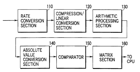
FIG. 6 is a block diagram schematically showing a
tone signal receiving apparatus according to the first
embodiment of the present invention.
As shown in FIG. 6, the tone signal receiving
apparatus according to the first embodiment comprises a
rate conversion section 110, compression/linear
conversion section 120, arithmetic processing section
130, absolute value conversion section 140, comparator
150, and matrix section 160.
The rate conversion section 110 is connected to a
voice bus (PCMHW) (not shown). The rate conversion
section 110 extracts one of a plurality of channels
multiplexed on the voice bus at one frame period (e. g.,
125 us) and lowers the rate to form continuous data.
That is, the rate conversion section 110 reproduces a
PCM signal whose value changes at a predetermined
period.
CA 02326873 2000-11-24
- 26 -
The compression/linear conversion section 120
receives the PCM signal output from the rate conversion
section 110. This PCM signal is compressed by one of
two kinds of compression schemes (~-255 rule and A
rule) shown in FIGS. 7A and 7B. Thus, the
compression/linear conversion section 120 expands the
PCM signal output from the rate conversion section 110
in accordance with the conversion scheme shown in
FIG. 7A or 7B to restore a linear PCM signal.
The arithmetic processing section 130 executes a
product-sum arithmetic operation (to be described later
in detail) for each of a total of eight frequencies
possibly contained in a DTMF signal using the PCM
signal at the current time, a PCM signal one sampling
period before, and a PCM signal two sampling periods
before, which are supplied from the compression/linear
conversion section 120. An arithmetic value obtained
by the arithmetic processing section 130 is supplied to
the absolute value conversion section 140.
The absolute value conversion section 140
calculates the absolute value of the output value from
the arithmetic processing section 130.
The comparator 150 extracts an output value equal
to or larger than a predetermined threshold value from
the output value from the absolute value conversion
section 140 and outputs the value to the matrix section
160. The matrix section 160 determines the type of
CA 02326873 2000-11-24
- 27 -
DTMF signal, i.e., which dial key on the telephone set
is pressed by the user, on the basis of at least two
output values from the comparator 150 and sends the
determination result to a CPU (not shown). Since the
arithmetic value by the arithmetic processing section
130 can be a positive or negative value, it must be
converted into an absolute value by the absolute value
conversion section 140.
A detailed circuit example of the arithmetic
processing section 130 will be described next with
reference to FIG. 8. The operation of the arithmetic
processing section 130 will be described with reference
to FIGS. 9A to 9C.
Referring to FIG. 8, the product-sum arithmetic
circuit in the arithmetic processing section 130
comprises a subtractor (SUB) 131, adder (ADD) 132,
delay element (FFO) 133, delay element (FF1) 134, and
multiplier (MUL) 135.
The subtractor 131 subtracts a value V(n-2) two
sampling periods before shown in FIG. 9C from an input
value X(n) shown in FIG. 9A and outputs the difference
to the adder 132. The adder 132 adds the output from
the subtractor 131 and the value V(n-1) one sampling
period before shown in FIG. 9B. The sum is a new
output value V(n), which is held by the delay element
133 and output at an arbitrarily settable sampling
period. The output value V(n-1) from the delay element
. CA 02326873 2000-11-24
- 28 -
133 is held by the delay element 134, output at an
arbitrarily settable sampling period, and then output
to the subtractor 131 as V(n-2). The output value
V(n-1) from the delay element 133 is multiplied by a
coefficient K(f) corresponding to a frequency contained
in the DTMF signal by the multiplier 135 and the
product is output to the adder 132.
That is, the output value V(n) is represented by
Vk(n) - K(f) x Vk(n-1) - Vk(n-2) + X(n)
K(f) - 2 x cos(2nk/N)
Vk(-1) - 0
Vk(-2) - 0
n = 0, 1, ~~~ N-1
The above product-sum arithmetic processing is
executed N times in one frame period, and the number of
times of arithmetic processing is counted by a counter
136. This count value is compared with a count value N
set for each frequency by a comparator 137. When the
count value counted by the counter 136 matches the
count value N, the comparator 137 resets the counter
136 and outputs an address value to a ROM 138.
The ROM 138 has a setting table, in which the
number of samples N and the coefficient K(f) corre-
sponding to each of the total of eight frequencies
possibly contained in a DTMF signal are stored, as
shown in FIG. 10, and the number of samples N and
coefficient K(f) are sequentially read out and output
. CA 02326873 2000-11-24
_ 29 _
on the basis of the address value output from the
comparator 137. The readout number of samples N is
supplied to the comparator 137, while the coefficient
K(f) is supplied to the multiplier 135. Upon receiving
a reset signal from the comparator 137, the counter 136
resets the held values in the delay elements 133
and 134.
FIG. 11 is a block diagram showing a detailed
circuit example of the comparator 150.
The comparator 150 comprises eight registers 1511
to 1518 and a comparison section 152. Peak values as
the arithmetic results for eight frequencies, which are
calculated by the arithmetic processing section 130,
are stored in the eight registers in units of
frequencies in accordance with the order from 1 to 8.
The comparison section 152 reads out the peak values
from the eight registers 1511 to 1518 in accordance
with the order from 1 to 8, compares each value with a
threshold value Th, and output a peak value equal to or
larger than the threshold value Th to the matrix
section 160 as "1". The comparison section 152 also
outputs a peak value smaller than the threshold value
to the matrix section 160 as "0".
The matrix section 160 has a determination circuit
161 and counting circuit 162, as shown in FIG. 12. The
determination circuit 161 has a discrimination table in
which discrimination data, i.e., digit values
CA 02326873 2000-11-24
- 30 -
corresponding to sets of two of all frequencies
possibly contained in a DTMF signal are stored, as
shown in FIG. 13. The determination circuit 161 reads
out a corresponding digit value from the discrimination
table on the basis of eight data output from the
comparator 150, and outputs it to the CPU (not shown).
Eight data output from the comparator 150 include at
least two codes representing logic "1". A digit value
is expressed by a binary code of four bits (DO to D3).
The determination circuit 161 outputs the determination
result to the counting circuit 162. The counting
circuit 162 counts the number of times of determination
result input and outputs the counting result to the CPU
as a digit value DV. The determination circuit 161
also executes determination processing such that the
eight data output for the comparator 150 exceeds the
threshold value.
The relationship between the above arrangement and
the conventionally used Goertzel algorithm will be
described next.
In the Goertzel algorithm, when a DTMF signal X(n)
is given as an input signal, the DTMF signal X(n) is
converted a value ~yk(N)~2 in the frequency axis in
accordance with the Fourier transform scheme. This
algorithm is basically the Fourier transform, and
therefore, two frequency spectra in the frequency
components contained in the input signal represent peak
CA 02326873 2000-11-24
- 31 -
values. Thus, the DTMF signal can be recognized, i.e.,
a pressed dial key can be identified on the basis of
the combination pattern of frequency components having
the peak values.
The DTMF signal contains a total of 16 frequency
spectra: a total of eight frequency spectra for eight
specific frequencies, i.e., four low-frequency
components and four high-frequency components, and
eight second harmonics of these eight frequencies, as
shown in FIG. 14. In the Goertzel algorithm, to
simultaneously appropriately detect only these 16
spectra, the number of samples N is set to 205 points,
and second harmonics are set to 201 points. The second
harmonics are simultaneously detected to discriminate
the signal from a human voice. This is called TALK OFF
detection. This TALK OFF can be realized by detecting
harmonic components. Since a DTMF signal contains few
second harmonics, the spectrum value of a second
harmonic is compared with a predetermined threshold
value and identified. This embodiment can cope with
TALK OFF by changing the value of the coefficient K,
allowing circuit scale reduction for TALK OFF.
When the Goertzel algorithm is directly
implemented by a digital circuit, a feed-forward loop
structure as shown in FIG. 15 is normally available.
The product-sum arithmetic device shown in FIG. 15
comprises a delay element 501, multiplier 502,
CA 02326873 2000-11-24
- 32 -
delay element 503, subtractor 504, adder 505, and
multiplier 506.
In the product-sum arithmetic device, a
product-sum arithmetic value one sampling period before,
which is delayed by the delay element 501, is
multiplied, by the multiplier 502, by a coefficient
determined in accordance with each frequency possibly
contained in a DTMF signal, thereby obtaining a first
reference value for each frequency. In addition, a
product-sum arithmetic value for each of a plurality of
frequencies two sampling periods before, which is
delayed by the delay element 503, is subtracted from
the current input signal by the subtractor 504, thereby
obtaining a second reference value for each reference
frequency. The first reference value and second
reference value are added by the adder 505. The sum is
supplied to the multiplier 506. The multiplier 506
controls the multiplier 502 to adjust such that the
frequency spectrum extraction result is obtained at the
final sampling point.
However, the above feed-forward loop structure
requires an extra circuit other than the feed-forward
loop.
In this embodiment, the product-sum arithmetic
circuit used in the arithmetic processing section 130
has a feedback loop structure including no feed-forward
loop structure, in which the Goertzel algorithm is
CA 02326873 2000-11-24
- 33 -
simplified, and peak hold processing is performed. In
addition, since the object is to recognize the type of
DTMF signal, the accuracy of an output value may be
lower. For downsizing, the number of product-sum
arithmetic bits is decreased to reduce the circuit
scale.
The product-sum arithmetic circuit in the
arithmetic processing section 130 executes processing
while changing the number of samples and coefficient in
units of frequencies and therefore can perform
arithmetic operation of a frequency close to a
detection frequency. To do this, an optimum number of
samples and coefficient K to be used for the arithmetic
operation are ensured in advance. The deviation of
each frequency must be 3~, i.e., a specification of a
currently used analog receiver. However, generally,
for the frequency deviation in the feedback loop
structure, the lower the frequency is, the larger the
bandwidth becomes, and the higher the frequency is, the
smaller the bandwidth becomes. For this reason, if the
number of samples remains the same, the deviation
changes between frequencies. To make uniform the
deviations of frequencies, the number of samples is set
to about 200 points for a low-frequency component to
reduce the bandwidth and to about 100 points for a
high-frequency component to increase the bandwidth.
Thus for a high-frequency component, an output value
CA 02326873 2000-11-24
- 34 -
can be obtained using 100 points: the value is output
in time 1/2 that required for the arithmetic operation
of a low-frequency component. This allows further
multiplexing.
FIG. 16 is a graph showing a change in output
value from the arithmetic processing section 130 at
each frequency when the above method and number of
samples are used. As a nature of an input signal, it
vibrates and increases the amplitude value at an
adapted frequency, while it attenuates at other
frequencies. Using this nature, the comparator 150 can
detect a value in a shorter time by peak-holding the
absolute value of the output value at each frequency
and comparing the peak value with a predetermined
threshold value, instead of waiting for a result until
the arithmetic operation for 200 points is ended, as
shown in FIG. 17. In addition, each frequency can be
separated without arithmetic operation for 200 points.
For this reason, when the arithmetic operation for 160
points is ended, the count is reset to 0, and the
arithmetic operation starts from 0. For 200 points,
only one arithmetic output is obtained within the
detection time of 40 ms. However, for 160 points, two
outputs values of arithmetic operation are obtained.
When the number of times of arithmetic operation is
decreased, the number of times of output increases, and
the accuracy increases.
CA 02326873 2000-11-24 ..
- 35 -
As described above, according to this embodiment,
the arithmetic processing section 130 has a product-sum
arithmetic circuit which implements the Goertzel
algorithm by a digital circuit. In this product-sum
arithmetic circuit, product-sum arithmetic processing
in which a value obtained by subtracting, from an input
signal, a product-sum arithmetic value two sampling
periods before as the output from the delay element 134
by the subtractor 131, and a value obtained by
multiplying a product-sum arithmetic value one sampling
period before as the output from the delay element 133
by a coefficient corresponding to a frequency possibly
contented in a DTMF signal by the multiplier 135 are
added by the adder 132 is repeatedly executed a number
of times equal to the number of samples corresponding
to each of the frequencies. For this reason, the
circuit can cope with an arbitrary frequency contained
in an actual DTMF signal without requiring any extra
dedicated circuit. When an output value equal to or
larger than a predetermined threshold value is
extracted, by the comparator 150, from the arithmetic
results by the product-sum arithmetic circuit, the
frequency spectrum contained in the DTMF signal can be
detected. On the basis of this detection result, the
type of DTMF signal can be determined by the matrix
section 160. That is, DTMF signal detection processing
is divisionally executed by the respective digital
CA 02326873 2000-11-24 .,
- 36 -
circuits so that DTMF signal detection processing
equivalent to the conventional processing using a codec
section and processing using a DSP can be realized.
For this reason, when the product-sum arithmetic
circuit having the Goertzel algorithm as a digital
circuit is used, creation of a program for executing
the Goertzel algorithm and a large-capacity memory for
storing the program are unnecessary. In addition, when
the DTMF signal detection processing is divisionally
executed by the respective digital circuits such as the
arithmetic processing section 130, comparator 150, and
matrix section 160, the process capacity of one digital
circuit can be lower. Hence, an increase in circuit
scale can be suppressed, allowing integration and cost
reduction.
The product-sum arithmetic circuit has a feedback
loop structure in which the Goertzel algorithm
arithmetic operation is simplified and limits numerical
value approximation and accuracy in the arithmetic
process. Hence, the circuit scale can be made small,
and an on-chip system can easily be implemented.
The product-sum arithmetic circuit shown in FIG. 8
has a circuit arrangement for one frequency. However,
a circuit arrangement capable of calculating, e.g.,
eight multiplexed frequencies can also be realized.
FIG. 18 is a circuit block diagram showing the
arrangement of the product-sum arithmetic circuit in
CA 02326873 2000-11-24
- 37 -
the arithmetic processing section 130 for executing the
multiplex arithmetic operation. FIG. 19 is a timing
chart showing the operation. The same reference
numerals as in FIG. 8 denote the same parts in FIG. 18,
and a detailed description thereof will be omitted.
Referring to FIG. 18, a first delay element group
1330 in which eight delay elements (FFO) 1331 to 1338
are connected in series is provided on the output side
of the adder 132, and a second delay element group 1340
in which eight delay elements (FF1) 1341 to 1348 are
connected in series is provided on the output side of
the first delay element group 1330.
In the first delay element group 1330, data of
8 TSs (TSO to TS7), which are output from the adder 132,
are input to the delay element 1331 and sequentially
shifted to the delay element 1338 by 1 TS. The data
are delayed by one sampling period as a whole and
output to the second delay element group 1340 and
multiplier 135. In the second delay element group 1340,
the data of 8 TSs (TSO to TS7) output from the first
delay element group 1330 are input to the delay element
1341 and sequentially shifted to the delay element 1348
by 1 TS at a period 1/8 the sampling period. The data
are delayed by one sampling period as a whole and
output to the adder 132. Note that the delay time set
in each delay element in the first delay element group
1330 and second delay element group 1340 can be
CA 02326873 2000-11-24
- 38 -
arbitrarily set in accordance with the frequency.
The subtractor 131 subtracts the output (FF1 - 8)
of the delay element 1348 for the input signal x(n).
The adder 132 adds the output from the subtractor 131
and a value obtained by multiplying the output
(FFO - 8) of the delay element 1338 by the coefficient
K(f) by the multiplier 135, and outputs the sum to
absolute value conversion section 140 and first delay
element group 1330. This arithmetic processing is
sequentially time-divisionally executed for the data
of 8 TSs a number of times equal to the number of
samples N.
In this case, the absolute value conversion
section 140, comparator 150, and matrix section 160 on
the output side execute time-divisional processing for
the data of 8 TSs.
In the above description, the arithmetic
processing is executed for the data of 8 TSs. However,
this processing can be similarly executed for data
which multiplexes another plurality of TSs by preparing
delay elements in number equal to the number of TSs in
the first delay element group 1330 and second delay
element group 1340.
(Second Embodiment)
The second embodiment of the present invention is
related to a tone signal transmitting apparatus for
time-divisionally generating a tone signal formed from
CA 02326873 2000-11-24
- 39 -
a plurality of types of waveforms in a key telephone
system.
FIG. 20 is a block diagram showing a tone signal
transmitting apparatus according to the second
embodiment of the present invention.
A tone signal transmitting apparatus 300 comprises
storage sections 310 and 320, sine wave generation
section 330, reset generation section 340, rectangular
processing section 350, addition/alternating processing
section 360, and compression section 370.
As shown in FIG. 21, the storage section 310
stores pieces of frequency information corresponding to
2n sine waves to generate two single frequencies per
waveform in accordance with an instruction from an
external control section 14 (to be described later).
The frequency information stored in the storage section
310 can be rewritten from the control section 14. The
storage section 320 stores pieces of amplitude
information corresponding to 2n sine waves to generate
two single frequencies per waveform in accordance with
an instruction from the control section 14. The
amplitude information stored in the storage section 320
can also be rewritten from the control section 14.
The sine wave generation section 330 outputs a
sine wave signal on the basis of frequency information
read out from the storage sections 310 and amplitude
information read out from the storage sections 320, in
CA 02326873 2000-11-24
- 40 -
accordance with an instruction from the control section
14. The reset generation section 340 resets the sine
wave generation section 330 at a predetermined interval
to stabilize the sine wave signal output from the sine
wave generation section 330. The rectangular
processing section 350 forms a rectangular wave from
the sine wave signal output from the sine wave
generation section 330 on the basis of amplitude
information stored in the storage section 320. The
addition/alternating processing section 360 executes
addition or alternating processing for the output from
the rectangular processing section 350. The
compression section 370 can switch between the A rule
and the ~ rule for different compression schemes on the
basis of a control signal from the control section 14.
The compression section 370 selectively compresses the
output from the addition/alternating processing section
360 on the basis of the A rule or ,u rule.
The sine wave generation section 330 will be
described first. As shown in FIG. 21, the sine wave
generation section 330 comprises latches 331, 332, and
333, a subtractor 334, and a multiplier 335.
The principle of sine wave oscillation by the sine
wave generation section 330 will be described. As is
known, according to the z-transform theory in signal
processing, sine wave oscillation can be described by
CA 02326873 2000-11-24 .
- 41 -
Y(0) - 2cosc~y(-1) - y(-2)
c~ - 2 ~ ~ (oscillation frequency) /sampling
frequency
initial value y(-1) - 0
y(-2) - Asinc~ (A is an amplitude
value)
The value 2cosc~ is held by the storage section
320 as amplitude information, and the value Asinc~ is
held by the storage section 310 as frequency
information. In the sine wave generation section 330,
after a reset signal is received, the value of the
latch 333 is set to 0, and the latch 331 is made to
hold amplitude information output from the storage
section 320. After that, the latch 333 receives the
output value from the latch 332 in synchronism with a
clock. At the same timing, the latch 331 receives the
output value from the latch 333.
The output data value from the latch 333 and
frequency information output from the storage section
310 are multiplied by the multiplier 335. The
subtractor 334 subtracts the data value from the latch
331 from a product data value as the output from the
multiplier 335. The output from the subtractor 334 is
received by the latch 332 in synchronism with a clock.
At the same timing, the data in the latch 332 moves to
the latch 333, and simultaneously, the data in the
latch 333 moves to the latch 331. By repeating such
CA 02326873 2000-11-24
- 42 -
operation, single frequency data can be continuously
generated.
In the sine wave generation section 330, 2n
latches 331 and 333 are cascade-connected to
time-divisionally generate data. In the latches 331
and 333, data is shifted to the next stage in
accordance with a clock to change stored data contents
one by one. Thus, 2n sine wave data are
time-divisionally output for one data. The time
required to output the first to final sine wave data is
defined as one frame.
FIG. 22 is a circuit block diagram showing the
arrangement of the reset generation section 340. The
reset generation section 340 comprises a timer 341, a
waveform sign monitor circuit 342 for finding a timing
when each waveform is to be smoothly restarted after a
time-up in the timer, a reset monitor register 343 for
storing whether reset is done after a time-up in the
timer, a 2-frame signal output register 344 for
generating a reset signal for forcibly resetting the
sine wave generation section 330 upon receiving an
external reset, a comparator 345, and an OR circuit 346.
The operation in the reset generation section 340
will be described. After a time-up in the timer 341,
the reset monitor register 343 outputs information
representing a time-up, i.e., logic value "1" to one
input terminal of the comparator 345. Information
CA 02326873 2000-11-24
- 43 -
representing a determination result from the waveform
sign monitor circuit 342 is output to the other input
terminal of the comparator 345. The waveform sign
monitor circuit 342 receives a sine wave signal
generated by the sine wave generation section 330,
stores the sign of one frame in a sign storage register
3421. In the waveform sign monitor circuit 342
compares the sign stored in the sign storage register
3421 with the sign of the sine wave signal as a current
frame, and outputs logic value "1" to the comparator
345 when the sign of the previous frame is +, and the
sign of the current frame is -.
When the two input signals represent logic value
"1", the comparator 345 outputs a signal representing
logic value "1" to the OR circuit 346. Upon receiving
the signal representing logic value "1" by one input
terminal, the OR circuit 346 generates a reset signal.
when an external reset signal is received, the 2-frame
signal output register 344 sends the reset signal to
the sine wave generation section 330 through the OR
circuit 346 and simultaneously reset the timer 341, so
that the timer 341 starts counting after the external
reset is canceled.
FIG. 23 is a circuit block diagram schematically
showing a detailed circuit example of the rectangular
processing section 350.
The rectangular processing section 350 comprises
CA 02326873 2000-11-24
- 44 -
latches 351 and 352 for storing a sine wave signal
generated by the sine wave generation section 330, a
latch 353 for storing amplitude information generated
from the storage section 320 as a fixed value, a
storage section 354 and register 355 which store
whether a sine wave signal or rectangular wave signal
is to be output, and a selector 356 for switching the
output in accordance with the register 355. The
latches 351 and 352 receive signals at different
timings whereby sine wave signal 1 is stored in the
latch 351, and sine wave signal 2 is stored in the
latch 352. Information stored in the storage section
354 can be rewritten by the control section 14.
The selector 356 selectively derives sine wave
signal 1 stored in the latch 351 or amplitude
information for the storage section 320, which is
stored in the latch 353. Note that the amplitude
information stored in the latch 353 is constant for a
sine wave and therefore has a fixed value for one sine
wave. To output a sine wave signal, the selector 356
directly selectively derives the output from the latch
351. To output a rectangular wave signal, the selector
356 replaces values other than the sign bit of the
output from the latch 351 with the fixed value from the
latch 353 and output the value, as shown in FIG. 24.
Since the sign changes at the same period as that of
the sine wave, and the amplitude value is constant, a
CA 02326873 2000-11-24
- 45 -
rectangular wave is formed. Thus, the rectangular
processing section 350 can output both a sine wave and
a rectangular wave. The selector 356 is ON/OFF-
controlled by the register 355, and information
representing whether rectangular processing is to be
executed for each tone is stored in the storage section
354. Hence, the register 355 reads the information
stored in the storage section 354 and switches the
selector 356 in accordance with the tone number.
FIG. 25 is a circuit block diagram showing a
detailed circuit example of the addition/alternating
processing section 360.
The addition/alternating processing section 360
comprises an adder 361 for adding two input signals, a
timer 362 and selector 363 for alternating processing,
a storage section 364 and register 365 which store
information representing which is to be output for each
tone, the output from the adder 361 or the output from
the selector 363, and a selector 366 for selectively
deriving the output from the adder 361 or the output
from the selector 363 in accordance with the output
from the register 365. Information stored in the
storage section 364 can be externally written.
The operation of the addition/alternating
processing section 360 having the above arrangement
will be described in detail with reference to FIGS. 26A
and 26B.
CA 02326873 2000-11-24
- 46 -
As shown in FIG. 26A, the adder 361 adds sine wave
signal 1 (or a rectangular wave signal) and sine wave
signal 2 and outputs the sum to the selector 366.
Parallel to the adder 361, the selector 363 is
executing alternating processing of alternately
switching between sine wave signal 1 (or a rectangular
wave signal) and sine wave signal 2 at a time interval
set in the timer 362 and outputting the signal, as
shown in FIG. 26B. The selector 366 selectively
derives the output from the adder 361 or the output
from the selector 363 in accordance with the output
from the register 365. Note that the register 365
reads information stored in the storage section 364 and
switches the selector 366 in accordance with the tone
number.
An operation of generating one waveform in the
tone signal transmitting apparatus will be described
next.
The sine wave generation section 330 generates
sine wave signal 1 and then sine wave signal 2. The
rectangular processing section 350 forms a rectangular
wave signal from sine wave signal 1 as needed. The
addition/alternating processing section 360 executes
alternating processing for the output from the
rectangular processing section 350 when an alternating
waveform is output, and otherwise, executes addition
processing. The compression section 370 compresses
CA 02326873 2000-11-24 ..
- 47 -
the output from the addition/alternating processing
section 360.
To generate a single-frequency waveform, the sine
wave generation section 330 generates sine wave signal
1 as the necessary single frequency and then oscillates
sine wave signal 2 at a frequency of 0 [Hz] and
amplitude of 0, the rectangular processing section 350
does not execute rectangular processing, the
addition/alternating processing section 360 adds sine
wave signal 1 and sine wave signal 2, and the
compression section 370 compresses the signal. To
generate a rectangular waveform, the storage section
320 is caused to store an amplitude value, the sine
wave generation section 330 generates sine wave signal
1 as a single frequency and then oscillates sine wave
signal 2 at a frequency of 0 [Hz] and amplitude of 0,
the rectangular processing section 350 executes
rectangular processing, the addition/alternating
processing section 360 adds the rectangular wave signal
and sine wave signal 2, and the compression section 370
compresses the signal.
The tone signal transmitting apparatus according
to the second embodiment is applied to the main
apparatus of a key telephone system, as shown in
FIG. 27. The same reference numerals as in FIG. 4
denote the same parts in FIG. 27, and a detailed
description thereof will be omitted.
CA 02326873 2000-11-24
- 48 -
In a main apparatus 1C, the control section 14 is
connected to the tone signal transmitting apparatus 300
and time switch section (TSW) 13. Data for each tone
and data representing the compression scheme are
written in the tone signal transmitting apparatus 300
by the control section 14, and speech communication
control is executed for the time switch section 13.
In this key telephone system, at the time of
activation, the control section 14 writes pieces
of frequency information, amplitude information,
rectangular processing information, addition/
alternating information, and ~ rule/A rule
compression information corresponding to necessary
tones in the respective storage sections in the tone
signal transmitting apparatus 300 and supplies a reset
signal. Thus the tone signal transmitting apparatus
300 starts time-divisionally generating a necessary
tone signal.
A case wherein a tone signal is to be output to an
extension terminal T1 will be described next. The time
switch section 13 can process a tone signal output from
the tone signal transmitting apparatus 300 in the same
way as that for a voice signal sent from the extension
terminal T1 because these signals has the same format.
Hence, the time switch section 13 switches the line
such that the tone signal generated by the tone signal
transmitting apparatus 300 is directly sent to the
CA 02326873 2000-11-24 ..
- 49 -
extension terminal T1. In addition, the tone signal
can be changed by rewriting data in the tone signal
transmitting apparatus 300 by the control section 14.
As described above, according to the second
embodiment, instead of having a memory storing waveform
information, the storage sections 310 which store
frequency information and the storage section 320 which
store amplitude information are used, and a sine wave
signal to be sent as a tone signal is generated by the
sine wave generation section 330 using a plurality of
types of frequency information and amplitude
information sequentially generated from the storage
sections 310 and 320. For this reason, the memory used
in the entire apparatus can be made small. In addition,
the waveform to be generated can easily be changed by
rewriting the frequency information in the storage
sections 310 and amplitude information in the storage
sections 320 on the basis of an external control signal.
In generating a waveform, the waveform changes due to a
calculation error. However, the sine wave output can
be stabilized by resetting the sine wave generation
section 330 at a predetermined interval by the reset
generation section 340.
The reset generation section 340 generates the
reset signal when the waveform sign monitor circuit 342
detects that the waveform generated by the sine wave
generation section 330 changes from + to - instead of
CA 02326873 2000-11-24
- 50 -
generating the reset signal immediately after the end
of counting by the timer 341. Hence, the sine wave
generation section 330 can be smoothly reset without
interrupting the output waveform.
The rectangular processing section 350 has the
storage section 354 and register 355 whose information
can be rewritten by external control, and the selector
356 capable of selectively deriving the amplitude value
of the sine wave signal or the fixed value stored in
the latch 353 in accordance with the output from the
register 355. This enables control to determine
whether the sine wave signal is to be converted into a
rectangular wave signal in accordance with an
instruction from the control section 14. A sine wave
can be generated using an amplitude value after
rectangular processing by selectively replacing the
amplitude value of the sine wave signal output from the
latch 351 and the fixed value output from the latch 353
by the selector 356. For this reason, the amplitude
value information storage device for rectangular
processing can be omitted.
The addition/alternating processing section 360
has the storage section 364 and register 365 whose
information can be rewritten on the basis of a control
signal from the control section 14, and the selector
366 for selectively deriving the output from the adder
361 or the output from the selector 363 in accordance
CA 02326873 2000-11-24
- 51 -
with the output from the register 365. Hence, addition
processing and alternating processing can easily be
switched in accordance with a tone signal to be
generated.
The compression section 370 can switch between the
A rule and the a rule for different compression schemes
on the basis of a control signal from the control
section 14 and selectively compresses the output from
the addition/alternating processing section 360 on the
basis of the A rule or ,u rule. Hence, the compression
scheme for a tone signal to be generated can be changed
anytime in accordance with an instruction from the
control section 14.
In the second embodiment, a tone signal having an
arbitrary waveform can easily be generated by rewriting
information in at least one of the storage sections 310
and 320, rectangular processing section 350, and
addition/alternating processing section 360 by the
control section 14.
(Third Embodiment)
In the third embodiment of the present invention,
the tone signal receiving apparatus of the first
embodiment shown in FIG. 6 and the tone signal
transmitting apparatus of the second embodiment shown
in FIG. 20 are integrated into a single tone signal
transmitting/receiving apparatus.
FIG. 28 is a block diagram schematically showing
. CA 02326873 2000-11-24 ..
- 52 -
the tone signal transmitting/receiving apparatus
according to the third embodiment of the present
invention. The same reference numerals as in FIG. 6
denote the same parts in FIG. 28, and a detailed
description thereof will be omitted.
Referring to FIG. 28, an arithmetic processing
section 400 selectively executes tone signal
transmission processing or tone signal reception
processing on the basis of a parameter generated by a
parameter generation section 600.
FIG. 29 is a block diagram schematically showing a
detailed circuit example of the arithmetic processing
section 400.
Referring to FIG. 29, a product-sum arithmetic
circuit 410 in the arithmetic processing section 400
comprises an adder 411, delay element (FFO) 412, delay
element (FF1) 413, multiplier 414, and subtractor 415.
The adder 411 adds a predetermined first reference
value for each of a plurality of reference frequencies
(e.g., 697 Hz, 770 Hz, 852 Hz, 941 Hz, 1209 Hz, 1336 Hz,
1477 Hz, and 1633 Hz) and a predetermined second
reference value for each of the plurality of reference
frequencies to calculate a product-sum arithmetic value
at the current time for each of the reference
frequencies. The product-sum arithmetic value is
supplied to a selector 420 and also held by the delay
element 412 for an arbitrarily settable sampling period
a CA 02326873 2000-11-24
- 53 -
and output. The output from the delay element 412 is
held by the delay element 413 for an arbitrarily
settable sampling period and output.
The multiplier 414 multiples the output value for
the delay element 412 by a coefficient determined in
accordance with each reference frequency to calculate
the first reference value for each reference frequency
and outputs it to the adder 411. The subtractor 415
calculates the second reference value from the output
value of the delay element 413 and outputs it to the
adder 411.
The product-sum arithmetic circuit 410 also has
selectors 421, 422, and 423. The selector 421 switches
between execution and stop of processing of setting the
output value from the delay element 413 to an initial
amplitude value determined using the frequency of a
tone signal to be generated in accordance with the tone
signal transmission processing mode or tone signal
reception processing mode. The selector 422 switches
the coefficient to be given to the multiplier 414 in
accordance with the tone signal transmission processing
mode or tone signal reception processing mode. The
selector 423 switches between execution and stop of
processing of giving an input signal to the subtractor
415 in accordance with the tone signal transmission
processing mode or tone signal reception processing
mode.
CA 02326873 2000-11-24
- 54 -
In the product-sum arithmetic circuit 410, in the
tone signal transmission processing mode, the selector
421 sets the output value from the delay element 413 to
the initial amplitude value determined in accordance
with the frequency of the tone signal to be generated,
the selector 422 gives to the multiplier 414 the
coefficient determined in accordance with the frequency
of the tone signal to be generated, i.e., the
oscillation frequency value, and the selector 423
derives the input value [0] to the subtractor 415, so
the subtractor 415 generates the second reference value
as the inverted value of the output value from the
delay element 413.
In the product-sum arithmetic circuit 410, in the
tone signal reception processing mode, the selector 423
inputs the output signal from a compression/linear
conversion section 120 to the subtractor 415, the
subtractor 415 subtracts the output value of the delay
element 413 from the input signal to calculate the
second reference value for each of the reference
frequencies, and the selector 422 gives the coefficient
determined in accordance with the reference frequency.
The selectors 420 to 423 are switched to tone
signal reception processing for three of a plurality of
periods obtained by equally dividing one frame period
(125 ,us) shown in FIG. 30 and switched to tone signal
transmission processing for one period obtained by the
CA 02326873 2000-11-24
- 55 -
equal division. One period obtained by the equal
division corresponds to the time required for
arithmetic processing of the product-sum arithmetic
circuit 410.
More specifically, in the arithmetic processing
section 400, in the tone signal transmission processing
mode, the first reference value obtained by multiplying
the output value from the delay element 412 by the
coefficient determined in accordance with the frequency
of the desired tone signal by the multiplier 414 and
the second reference value obtained by inverting the
output value from the delay element 413 by the
subtractor 415 are added by the adder 411 whereby the
tone signal to be transmitted is obtained and
selectively derived by the selector 420. This tone
signal is output to a PCMHW (not shown) and also
supplied to the parameter generation section 600. When
the elapse time from the previous reset exceeds a
predetermined time, and the polarity of the digital
value of the tone signal changes from + to -, the
parameter generation section 600 resets the output
value from the delay element 412 to [0] and the output
value from the delay element 413 to the initial
amplitude value determined according to the frequency
of the tone signal in accordance with the absolute
value of the output digital value.
Additionally, in the arithmetic processing section
CA 02326873 2000-11-24
- 56 -
400, in the tone signal reception processing mode, the
first reference value for each of the reference
frequencies is obtained by multiplying the output value
from the delay element 412 by the coefficient
determined in accordance with the reference frequency
by the multiplier 414 and the second reference value
for each of the reference frequencies is obtained by
subtracting the output value of the delay element 413
from the current input signal by the subtractor 415 and
product-sum arithmetic processing of adding by the
adder 411 the first reference value for each of the
reference frequency and the second reference value for
each of the reference is repeatedly executed for the
respective reference frequencies. The product-sum
arithmetic value calculated for each of the reference
frequencies is derived at an absolute value conversion
section 140 by the selector 420 and converted into
an absolute value by the absolute value conversion
section 140, a peak value equal to or larger than a
predetermined threshold value is extracted by a
comparator 150, and the type of, e.g., a DTMF signal is
determined by a matrix section 160 on the basis of at
least two extracted peak values.
As described above, in the third embodiment, the
product-sum arithmetic circuit 410 which implements the
Goertzel algorithm by a digital circuit is shared by
tone signal transmission processing and tone signal
CA 02326873 2000-11-24
_ 57 _
reception processing. In accordance with the tone
signal transmission processing mode or tone signal
reception processing mode, an input signal is given to
the subtractor 415 in the product-sum arithmetic
circuit 410, a coefficient is given to the multiplier
414, and the initial amplitude value is selectively set
in the delay element 413.
Hence, the product-sum arithmetic circuit 410 need
not be separately prepared for tone signal transmission
processing and tone signal reception processing. In
addition, in the tone signal transmission processing
mode, a tone signal having a desired frequency can be
generated only by setting the output value from the
delay element 413 in the product-sum arithmetic circuit
410 to the initial amplitude value determined in
accordance with the frequency of the tone signal to
be generated, giving a coefficient determined in
accordance with the frequency of the tone signal to be
generated to the multiplier 414, and generating the
second reference value by inverting the output value
from the delay element 413 by the subtractor 415.
Furthermore, in the tone signal reception processing
mode, a plurality of frequency spectra including each
reference frequency as the center frequency can be
detected from an input signal only by giving the input
signal to the subtractor 415, subtracting the output
value of the delay element 413 from the input signal by
CA 02326873 2000-11-24
- 58 -
the subtractor 415 to calculate the second reference
value for each of the reference frequencies, and giving
a coefficient determined in accordance with the
reference frequency to the multiplier 414. The type of
tone signal can be determined on the basis of the
detection result.
For this reason, the circuit scale can be reduced
in the entire system, and downsizing and reduction of
cost and power consumption by integration can easily be
realized. In addition, it is convenient because the
tone signal receiving apparatus or tone signal
transmitting apparatus can be selectively used in a
single apparatus, as needed.
In the third embodiment, since the selectors 420
to 423 are set to alternately switch between the tone
signal transmission processing mode and the tone signal
reception processing mode at a predetermined period,
switching control can be automatically executed without
manual operation.
In the third embodiment, in the tone signal
reception processing mode, the type of tone signal
received can be determined by the comparator 150 and
matrix section 160 from the product-sum arithmetic
value obtained by the product-sum arithmetic
circuit 410.
In the third embodiment, the product-sum
arithmetic processing for each of the plurality of
CA 02326873 2000-11-24
- 59 -
reference frequencies may be time-divisionally executed.
In this case, each delay element only need have a
multi-stage structure corresponding to the number of
reference frequencies, and the adder 411, multiplier
414, and subtractor 415 can be shared by the respective
reference frequencies. Hence, the circuit scale can be
further reduced as compared to a case wherein the
components are individually prepared.
In the third embodiment, only a tone signal having
one frequency is generated. However, a tone signal
having a plurality of frequencies may be
time-divisionally generated. More specifically, the
delay elements 412 and 413 are designed to have a
multi-stage structure, coefficients to be multiplied by
the multiplier 414 are time-divisionally given, and
different initial amplitude values are set for the
respective delay elements in accordance with the
frequency.
In the third embodiment, only tone signal
reception for one channel is performed. However, tone
signal reception for a plurality of channels may be
time-divisionally performed. In this case, the product
of the number of reference frequencies and the number
of channels to be time-divisionally processed is used
as a variable. Additionally, in this case, the
arithmetic processing section 400, absolute value
conversion section 140, comparator 150, and matrix
CA 02326873 2000-11-24
- 60 -
section 160 also execute time-divisional processing.
If 100 lines are accommodated, and tone signal
transmitting/receiving apparatuses for eight channels
are required, a single tone signal transmitting/
receiving apparatus suffices to time-divisionally
process the eight channels. This greatly contributes
to a decrease in circuit scale, and accordingly, cost
reduction and downsizing, and reduction of power
consumption.
(Other Embodiments)
The present invention is not limited to the above
embodiments. In the above embodiments, a key telephone
system has been described. However, the present
invention can also be applied to a digital private
branch exchange system.
In the first and third embodiments, an example in
which a DTMF signal is processed has been described.
In addition to the DTMF signal, a tone signal formed by
arbitrarily combining g (g is an integer ? 2)
predetermined reference frequencies may be processed.
The arrangement of the arithmetic processing
section, the arrangement of the comparator, the
arrangement of the matrix section, and the arrangements
of the respective sections in the tone signal
transmitting apparatus can also be modified without
departing from the spirit and scope of the present
invention.
, CA 02326873 2000-11-24
- 61 -
As has been described above, according to the
present invention, a product-sum arithmetic circuit
which implements the Goertzel algorithm by a digital
circuit is used to discriminate a tone signal, and an
appropriate number of samples and coefficient
corresponding to each of all frequencies possibly
contained in the tone signal are sequentially given to
the product-sum arithmetic circuit. Thus the apparatus
can cope with an arbitrary frequency contained in an
actual tone signal. When an output value equal to or
larger than a predetermined threshold value is
extracted from the arithmetic result obtained by the
product-sum arithmetic circuit, two or more frequencies
contained in the tone signal can be detected, and the
type of tone signal can be determined on the basis of
the detection result.
According to the present invention, the device for
discriminating a tone signal can be constructed by a
digital circuit. Thus, a tone signal receiving
apparatus capable of suppressing an increase in circuit
scale, reducing the cost, forming a one-chip structure,
and also reducing the power consumption can be provided.
In addition, a tone signal receiving apparatus which
has a small chip area by circuit scale reduction and is
advantageous in constructing an on-chip system for
integrating other circuits can be provided.
According to another invention, instead of
CA 02326873 2000-11-24
- 62 -
preparing a memory storing waveform information,
memories which store amplitude information and
frequency information, respectively, are used, a
plurality of types of amplitude information and
frequency information stored in these memories are
sequentially read out to generate a sine wave signal to
be sent as a tone signal. In addition, the apparatus
is constructed by a selector for selectively replacing
the amplitude value of a sine wave signal with a fixed
value under external control, an output selector for
selectively deriving an addition output or an
alternating output, and a selector for switching
between the first compression rule and the second
compression rule for different compression schemes.
Hence, according to another invention, a tone
signal transmitting apparatus capable of reducing the
memory capacity and also flexibly coping with a change
in frequency and amplitude value of a waveform, a
change in data compression scheme, and switching
between 2-frequency addition and 2-frequency
alternating in an output waveform can be provided.
According to still another invention, a
product-sum arithmetic device which constitutes the
Goertzel algorithm by a digital circuit is shared by
tone signal transmission processing and tone signal
reception processing, and the coefficient and parameter
are selectively given to the subtractor, multiplier,
CA 02326873 2000-11-24
- 63 -
and the second delay element in the product-sum
arithmetic device.
Hence, according to still another invention, since
the product-sum arithmetic device need not be
separately prepared for tone signal transmission
processing and tone signal reception processing, an
increase in circuit scale can be suppressed in the
entire system, and downsizing and reduction of cost and
power consumption by integration can easily be realized.
In addition, it is convenient because the tone signal
receiving apparatus or tone signal transmitting
apparatus can be selectively used in a single apparatus,
as needed.
Additional advantages and modifications will
readily occur to those skilled in the art. Therefore,
the invention in its broader aspects is not limited to
the specific details and representative embodiments
shown and described herein. Accordingly, various
modifications may be made without departing from the
spirit or scope of the general inventive concept as
defined by the appended claims and their equivalents.