Note: Descriptions are shown in the official language in which they were submitted.
CA 02327108 2000-10-03
WO 00/55878 PCT/US99/23129
ELECTROMECHANICAL S~nTITCIiING DEVICE PACKAGE
wiTx corITROLLED ~rt»DANC>mtoNr~T
TECHNICAL FIELD
The present invention relates generally to switching devices.
More specifically, the present invention relates to improved
packaging and circuit integration for electromagnetic devices, such
as reed switches and electromagnetic devices such as reed relays.
BACKGROUND ART
Electromagnetic relays have been known in the electronics
industry for many years. Such electromagnetic relays include the
reed relay~'which incorporates a reed switch. A reed switch is a
magnetically activated device that typically includes two flat
contact tongues which are merged in a hermetically sealed glass
tube filled with a protective inert gas or vacuum. The switch is
operated by an externally generated magnetic field, either from a
coil or a permanent magnet. When the external magnetic field is
enabled, the overlapping contact tongue ends attract each other and
ultimately come into contact to close the switch. When the magnetic
field is removed, the contact tongues demagnetize and spring back
to return to their rest positions, thus opening the switch.
Reed switches, actuated by a magnetic coil, are typically
housed within a bobbin or spool-like member. A coil of wire is
wrapped about the outside of the bobbin and connected to a source
of electric current. The current flowing through the coil creates
the desired magnetic field to actuate the reed switch within the
bobbin housing. Some applications of reed devices require the
switch to carry signals with frequencies in excess of 500 MHz. For
these applications, a ground shield conductor, commonly made of
copper or brass is disposed about the body of the reed switch. The
ground shield conductor is commonly in a cylindrical configuration.
The shield conductor resides between the reed switch and the bobbin
housing to form a co-axial high frequency transmission system. This
co-axial system includes the outer shield conductor and the. switch
lead signal conductor co-axially through the center of the reed
switch. The ground shield conductor is employed to contain the
signal through the switch conductor in order to maintain the
desired impedance of the signal path.
Currently available reed devices are then incorporated into a
90 given circuit environment by users. For application at higher
frequencies, a reed switch device must be ideally configured to
SUBSTITUTE SHEET (RULE 26)
CA 02327108 2000-10-03
WO 00/55878 PCT/US99/23129
2
match as closely as possible the desired impedance requirements of
the circuit in which it is installed.
Within a circuit environment, a co-axial arrangement is
preferred throughout the entire environment to maintain circuit
integrity and the desired matched impedance. As stated above, the
body of a reed switch includes the necessary co-axial environment.
In addition, the signal trace on the user's circuit board commonly
includes a "wave guide" where two ground leads reside on opposing
sides of the signal lead and in the same plane or a "strip line"
where a ground plane resides below the plane of the signal
conductor. These techniques properly employed provide a two-
dimensional co-axial-like environment which is acceptable for
maintaining the desired impedance for proper circuit function.
However, the reed switch device must be physically packaged
and electrically interconnected to a circuit board carrying a given
circuit configuration. It is common to terminate the shield and
signal terminals to a lead frame architecture and enclose the
entire assembly in a dielectric material like plastic for
manufacturing and packaging ease. These leads may be formed in a
gull-Wing or "J"' shape for surface mount capability. The signal
leads or terminals exit out of the reed switch body and into the
air in order to make the electrical interconnection to the circuit
board. This transition of the signal leads from plastic dielectric
to air creates an undesirable discontinuity of the protective co-
axial environment found within the body of the switch itself. Such
discontinuity creates inaccuracy and uncertainty in the impedance
of the reed switch device. As a result, circuit designers must
compensate for this problem by specifically designing their
.~ircuits to accommodate and anticipate the inherent problems
associated with the discontinuity of the protective co-axial
'=.x;
environment and the degradation of the rated impedance of the reed
switch device. For example, the circuit may be tuned to compensate
for the discontinuity by adding parasitic inductance and
capacitance. This method of discontinuity compensation is not
preferred because it complicates and slows the design process and
can degrade the integrity of the circuit. There is a demand to
reduce the need to tune the circuit as described above. None of
the prior . art attempts address the problem of co-axial
discontinuity and impedance matching integrity.
In view of the foregoing, there is a demand for a reed switch
device that includes a controlled impedance environment through the
SUBSTITUTE SHEET (RULE l6)
CA 02327108 2006-12-28
21519-661
3
entire body of the package to the interconnection to a circuit.
There is further a demand for reed switch devices that are of a
surface mount configuration to optimize the high frequency of the
performancE of the system. Further, there is a demand for a reed
switch device that can reduce the need to tune a circuit to
compensate for an uncontrolled impedance environment. Also, there
is a demand for a reed switch device that has a small footprint and
is of a standard shape and configuration for simplified
installation.
DISCLOSURE OF THE IPdVENTION
The present invention preserves the advantages of prior art
electromagnetic switch devices, such as reed relays. In addition,
it provides new advantages not found in currently available
switching devices and overcomes many disadvantages of such
currently available devices.
The invention is generally directed to the novel and unique
reed switch device with particular application in effectively
interconnecting a reed switch device to a circuit on a circuit
board. The reed switch package of the present invention enables
the efficient and effective interconnection to a circuit board
while being in an inexpensive construction.
A reed switch device is disclosed that includes a reed switch
wii-h at least one electrical signal path. A cylindrical ground
shield is provided about the reed switch. Ground terminals are
connected to opposing sides of the ground shield so that the ground
terminals are on opposing sides of the signal terminal and lie in
the same plane. The reed switch resides on a support substrate.
An electrically conductive signal via extends through said main
body and connects to the signal terminal. Ground vices extend
throug2u the main body and respectively connect to the ground
terminals. The grounds vices are on opposing sides of the signal
vi.a and lie in the same plane as the signal via. The signal and
ground vi.a exit at the bottom of the main body and are connected to
a circuit via solder balls to provide a compact surface mount
package with a controlled impedance environment.
CA 02327108 2006-12-28
21519-661
3a
According to one aspect of the present invention,
there is provided a reed device package, comprising: a reed
switch having electrical signal terminals; a ground shield
surrounding said reed switch; a first ground terminal
connected to said ground shield; a second ground terminal
connected to said ground shield; at least one of said
electrical signal terminals being positioned between said
first ground terminal and said second ground terminal; a
support substrate having a main body with a top surface and
a bottom surface; said reed switch device being disposed on
said support substrate; an electrically conductive signal
via extending through said main body between said top
surface and said bottom surface; said signal via being
electrically connected to said electrical signal terminals
of said reed switch; an electrically conductive first ground
via extending through said main body between said top
surface and said bottom surface; said first ground via being
electrically connected to said first ground terminal; said
first ground via being positioned substantially parallel to
and in spaced apart relation to said signal via; an
electrically conductive second ground via extending through
said main body between said top surface and said bottom
surface; said second ground via being electrically connected
to said second ground terminal; said second ground via being
positioned substantially parallel to and in spaced apart
relation to said signal via and on an opposing side of said
signal via as said first ground via; means for
interconnecting said signal via, at said bottom surface of
said main body, to a signal line of a circuit; means for
interconnecting said first ground via, at said bottom
surface of said main body, to a first ground line of a
circuit; and means for interconnecting said second ground
via, at said bottom surface of said main body, to a second
ground line of a circuit.
CA 02327108 2006-12-28
21519-661
3b
According to another aspect of the present
invention, there is provided a reed device package,
comprising: a reed switch having electrical signal
terminals; a ground shield surrounding said reed switch; a
first ground terminal connected to said ground shield; a
second ground terminal connected to said ground shield; at
least one of said electrical signal terminals being
positioned between said first ground terminal and said
second ground terminal; a support substrate having a main
body with a top surface and a bottom surface; said reed
switch device being disposed on said support substrate; a
loop of electrically conductive material on said top surface
of said main body; said loop of electrically conductive
material interconnecting said first ground via and said
second ground via and being substantially co-axially
positioned about said signal via; an electrically conductive
signal via extending through said main body between said top
surface and said bottom surface; said signal via being
electrically connected to one of said electrical signal
terminals of said reed switch; a plurality of electrically
conductive ground vias extending through said main body
between said top surface and said bottom surface; said
plurality of ground vias being electrically connected to
said loop of electrically conductive material on said top
surface; said plurality of ground vias being positioned
substantially parallel to and surrounding said signal via;
means for interconnecting said signal via, at said bottom
surface of said main body, to a signal line of a circuit;
and means for interconnecting said plurality of ground vias,
at said bottom surface of said main body, to a ground line
of a circuit.
According to still another aspect of the present
invention, there is provided a reed device package,
CA 02327108 2006-12-28
21519-661
3c
comprising: a reed switch having a first end and a second
end; a first electrical signal terminal connected to said
first end of said reed switch; a second electrical signal
terminal connected to said second end of said reed switch; a
substantially cylindrical ground shield, having a
longitudinal axis, housing said reed switch; said
cylindrical ground shield including a first open end edge
and a second open end edge; a first ground terminal
connected to a region of said first open end edge; a second
ground terminal connected to a region of said first open
edge across from said first ground terminal; a third ground
terminal connected to a region of said second open edge; a
fourth ground terminal connected to a region of said second
open edge across from said third ground terminal; a support
substrate having a main body with a top surface and a bottom
surface; said reed switch device being disposed on said
support substrate; a first electrically conductive signal
via extending through said main body between said top
surface and said bottom surface; said first signal via being
electrically connected to said first electrical signal
terminal of said reed switch; a second electrically
conductive signal via extending through said main body
between said top surface and said bottom surface; said
second signal via being electrically connected to said
second electrical signal terminal of said reed switch; an
electrically conductive first ground via extending through
said main body between said top surface and said bottom
surface; said first ground via being electrically connected
to said first ground terminal; said first ground via being
positioned substantially parallel to and in spaced apart
relation to said first signal via; an electrically
conductive second ground via extending through said main
body between said top surface and said bottom surface; said
second ground via being electrically connected to said
CA 02327108 2006-12-28
21519-661
3d
second ground terminal; said second ground via being
positioned substantially parallel to and in spaced apart
relation to said first signal via and on an opposing side of
said first signal via as said first ground via; an
electrically conductive third ground via extending through
said main body between said top surface and said bottom
surface; said third ground via being electrically connected
to said third ground terminal; said third ground via being
positioned substantially parallel to and in spaced apart
relation to said second signal via; an electrically
conductive fourth ground via extending through said main
body between said top surface and said bottom surface; said
fourth ground via being electrically connected to said
fourth ground terminal; said fourth ground via being
positioned substantially parallel to and in spaced apart
relation to said second signal via and on an opposing side
of said second signal via as said third ground via; means
for interconnecting said first signal via, at said bottom
surface of said main body, to a first signal line of a
circuit; means for interconnecting said second signal via,
at said bottom surface of said main body, to a second signal
line of a circuit; means for interconnecting said first
ground via, at said bottom surface of said main body, to a
first ground line of a circuit; means for interconnecting
said second ground via, at said bottom surface of said main
body, to a second ground line of a circuit; means for
interconnecting said third ground via, at said bottom
surface of said main body, to a third ground line of a
circuit; and means for interconnecting said fourth ground
via, at said bottom surface of said main body, to a fourth
ground line of a circuit.
According to yet another aspect of the present
invention, there is provided a reed device package,
CA 02327108 2006-12-28
21519-661
3e
comprising: a first reed switch having a first and second
electrical signal terminals; a second reed switch having a
first and second electrical signal terminals; a ground
shield, having a first end and a second end, surrounding
said first reed switch; a plurality of ground terminals
connected to said ground shield at said first end of said
first ground shield; a plurality of ground terminals
connected to said ground shield at said second end of said
ground shield; a support substrate having a main body with a
top surface and a bottom surface; said first reed switch and
said second reed switch being disposed on said support
substrate; a first electrically conductive signal via
extending through said main body between said top surface
and said bottom surface; said first signal via being
electrically connected to said first electrical signal
terminal of said first reed switch; a second electrically
conductive signal via extending through said main body
between said top surface and said bottom surface; said
second signal via being electrically connected to said
second electrical signal terminal of said first reed switch;
a third electrically conductive signal via extending through
said main body between said top surface and said bottom
surface; said third signal via being electrically connected
to said first electrical signal terminal of said second reed
switch; a fourth electrically conductive signal via
extending through said main body between said top surface
and said bottom surface; said fourth signal via being
electrically connected to said second electrical signal
terminal of said second reed switch; a first plurality of
electrically conductive ground vias extending through said
main body between said top surface and said bottom surface;
said first plurality of ground vias respectively being
electrically connected to said plurality of ground terminals
connected to said ground shield at said first end of said
CA 02327108 2006-12-28
21519-661
3f
ground shield; said first plurality of electrically
conductive ground vias substantially surrounding said first
electrically conductive signal via; a second plurality of
electrically conductive ground vias extending through said
main body between said top surface and said bottom surface;
said second plurality of ground vias respectively being
electrically connected to said plurality of ground terminals
connected to said ground shield at said second end of said
ground shield; said second plurality of electrically
conductive ground vias substantially surrounding said second
electrically conductive signal via; means for
interconnecting said second electrical signal terminal of
said second reed switch to said second electrical signal
terminal of said first reed switch disposed on said bottom
surface of said main body; a first input terminal connected
to said first electrically conductive signal terminal of
said first reed switch; a second input terminal connected to
said first electrically conductive signal terminal of said
second reed switch; and an output terminal connected to said
second electrically conductive signal terminal of said first
reed switch.
It is therefore an object of the present invention
to provide a compact reed switch package.
It is an object of the present invention to
provide a reed switch device with a controlled impedance
environment throughout the entire package.
CA 02327108 2000-10-03
WO 00/55878 PCT/US99/23129
4
It is a further object of the present invention to provide a
reed switch package that is easily matched to the impedance of an
existing circuit environment.
Another object of the present invention is to provide a reed
switch package that is capable of efficiently conducting high
frequency signals.
It is a further object of the present invention to provide a
reed switch package that is inexpensive to manufacture.
It is yet a further object of the present invention to
provide a reed switch package with a small footprint.
Another object of the present invention is to provide a reed
switch package that employs a standardize BGA configuration and
body size.
SUBSTITUTE SHEET (RULE 26)
CA 02327108 2000-10-03
WO 00/55878 PCTNS99/23129
BRIEF DESCRIPTION OF THE DRAWINGS
The novel features which are characteristic of the present
invention are set forth in the appended claims. However, the
invention's preferred embodiments, together with further objects
5 and attendant advantages, will be best understood by reference to
the following detailed description taken in connection with the
accompanying drawings in which:
Fig. 1 is a perspective view of a prior art reed switch
configuration:
Fig. 2A is an perspective view a reed switch device in
accordance with the preferred embodiment of the present invention
Fig. 2B is an exploded perspective view a reed switch device
in accordance with the preferred embodiment of the present
invention shown in Fig. 2A;
Fig. a is a perspective view of the reed switch package with
a portion broken away for illustration purposes;
Fig. 4 is a cross-sectional view through the line 4-4 of Fig.
3 illustrating the mounting of the reed switch device within the
housing in accordance with the present invention:
Fig. 5 is a cross-sectional view through the line 4-4 of Fig.
4:
4;
4:
4;
Fig. 6 is a cross-sectional view through the line S-5 of Fig.
Fig. 7 is a cross-sectional view through the line 6-6 of Fig.
Fig. 8 is a cross-sectional view through the line 7-7 of Fig.
Fig. 9 is a perspective view of an alternative embodiment of
the reed switch package of the present invention with a portion
broken away for illustration purposes:
Fig. 10 is a cross-sectional view through the line 10-10 of
Fig. 9;
Fig. 11 is a cross-sectional view through the line 11-11 of
Fig. 10;
Fig. 12 is a cross-sectional view through the line 12-12 of
Fig. 10:
Fig. 13 is a cross-sectional view through the line 13-13 of
Fig. 10;
Fig. 14 is a cross-sectional view through the line 14-14 of
Fig. 10;
SUBSTITUTE SHEET (R ULE 26)
CA 02327108 2000-10-03
WO 00/55878 PCT/US99/Z3129
6
Fig. 15 is a cross-sectional view through the line 15-15 of
Fig. 10;
Fig. 16 is a diagram of a circuit employing the present
invention;
Fig. 17 is a cross-sectional view through a reed switch
device of the present invention carrying out the circuit shown in
Fig. 16; and
Fig. 18 is a bottom view of a reed switch device of the
present invention shown in Fig. 17.
MODES FOR CARRYING OUT THE INVENTION
Turning first to Fig. 1, a perspective view of a prior art
reed switch configuration 10 is shown. A known reed switch 11
includes a glass envelope 12 as well as two signal leads 14
emanating from opposing ends of the reed switch 11. The
construction of a reed switch 11 is so well known in the art, the
details thereof need not be discussed. A shield conductor 16,
commonly made of brass or copper, is provided in the form of a
cylindrical sleeve which receives and houses the reed switch 11.
The reed switch 11 and shield 16 are housed within the central bore
18 of a bobbin or spool 20. About the bobbin 20 ~is wound a
conductive wire 22. As a result, a co-axial arrangement is formed
to protect the reed switch 11 device and to controlled the
impedance of the environment and to improve the overall
transmission of the signal. The reed switch 11, shield conductor
16 and bobbin 20 are shown general as cylindrical in configuration.
It should be understood that various other configurations, such as
those oval in cross-section, may be employed and still be within
the scope of the present invention.
As can be understood and known in the prior art, the free
ends of the coil of wire 22, the shield 16 and signal terminals 14
of the reed switch 11 are electrically interconnected to a circuit
as desired. The respective components of the reed switch 11
configuration are interconnected to a circuit by lead frame or
other electrical interconnection (not shown). The lead frame or
other electrical interconnection introduces a discontinuity of the
desirable co-axial environment.
As described above, the overall reed switch device 10 must be
designed to be easily accommodated within a user's circuit. For
example, a circuit used to operate at high frequency is designed
with a defined characteristic impedance environment. The goal of
designing and manufacturing a reed device 10 to the specifications
SUBSTITUTE SHEET (R ULE 26)
CA 02327108 2000-10-03
WO 00/55878 PCT/US99l23129 .
7
of a circuit customer is to as closely as possibly match the
desired impedance of the device 10 to the circuit environment. It
is preferred that there is no discontinuity of impedance from the
reed device 10 itself to a circuit board trace of the circuit that
will receive the device 10. The characteristic impedance Z1 is,
generally, a function of the outer diameter of the signal conductor
14, the inner diameter of the shield 16 and the dielectric constant
of the insulation (not shown) between the signal conductor 14 and
the shield 16.
Turning now to Figs. 2-8, the preferred embodiment of the
present invention is shown. Referring to Fig. 2A, a modified reed
device 103 is provided to include an outer bobbin 102 with coil 109
wrapped therearound for introducing the necessary magnetic field to
actuate the reed switch 111. Ends of wire 109 may be connected to
posts 113 of bobbin 102. Emanating from the reed switch 111 are
two signal leads 106 which correspond to opposing sides of the reed
switch 111. Also emanating from the bobbin body 102 are a pair of
shield or ground tabs 108 on each side of the bobbin body 102 that
are electrically interconnected to, as shown in Fig. 6, the ends of
the inner shield sleeve 110. As shown in Fig. 2B, these giound
tabs 108 are extensions of from the shield sleeve 110 itself on
opposing sides thereof.
Referring to Fig. 3, a perspective view of the reed switch
package 100 with housing is shown. This complete reed switch
package 100 includes a substrate base 112 along with a number of
contact pads 114 for receiving the signal lead 106 and ground leads
108 from the reed switch 111. A metal or non-metallic shell 116 is
secured to the substrate base 112 with, for example, a bead of
epoxy (not shown) around the perimeter to provide a liquid-tight
seal. The entire assembly may be otherwise overmolded with
plastic.
Turning now to Fig. 4, a cross-sectional view through the
line 4-4 of Fig. 3 is shown. In particular, Fig. 4 illustrates in
detail the positioning of the reed device 103 on the substrate base
1I2. The substrate base 112 includes a recessed central portion
118 for receiving the bobbin portion 102 of the reed device 103 to
provide a short, straight signal path and reduce the overall size
of the package 100. Contact pads 120 are provided at a seat
portion 122 of the substrate base 112 to connect the signal leads
106 and ground leads 108. The reed device 103 is relatively light
in weight so as to be supported entirely by the signal lead 106 and
SUBSTITUTE SHEET (RULE 26)
CA 02327108 2000-10-03
WO 00/55878 PCT/US99/23129 ~
8
ground leads 108. However, other base substrate housings may be
employed (not shown) where the bobbin 102 rests on its own seat or
where additional contoured portions of the substrate 112 are
provided to support the reed device 103.
As will be described in detail below, signal leads 106 and
ground leads 108 are electrically interconnected to solder balls
124 for further electrical interconnection to a circuit on a
circuit board (not shown). Along with the protective shell 116 (or
solid encapsulant), a compact reed switch package 100 is provided
that is of a surface mount configuration to accommodate high
frequency reed switches 111 in a controlled impedance environment.
Figs. 4 and 5 further illustrate the details of the
construction of the reed switch 111 itself. In particular, the
reed switch 111 includes a signal conductor 106 within a glass
capsule 126 with an inert gas or vacuum 128 therebetween.
Positioned about the glass capsule 126 is a ground shield 130 which
is preferably of a cylindrical or tubular configuration but may be
of an oval cross-section to accommodate certain reed switches 111
or multiple reed switches in a multiple channel environment. The
foregoing assembly is housed within the bobbin 102 which includes
an energizing coil 109 therearound. The free ends of the
energizing coil 109 are connected to posts 113 which are
electrically connected to corresponding solder balls 124 on the
bottom surface 132 of the substrate base 112.
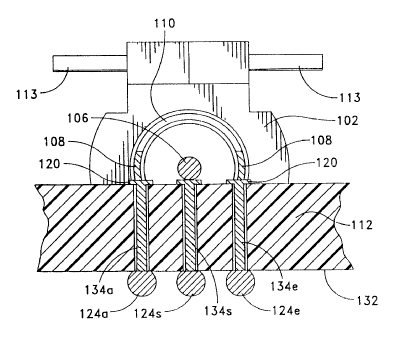
In addition, as shown in Figs 6-8, the contact pads 120 are
electrically interconnected to corresponding solder balls 124 on
the bottom surface 132 of the substrate base 112. Referring to
Fig. 6, a cross-section through the line 6-6 of Fig. 9, details of
the important interconnection of the signal leads 106 and ground
leads 108, via the contact pads 120 to the solder balls 124, is
shown. In particular, Fig. 6 illustrates one side of the reed
switch package 100. It should be understood that the construction
and details of the opposing side of the reed switch package 100 is
identical. For simplicity and ease of illustration only one side
of the reed switch package 100 will be discussed.
The signal leads 106 and ground leads 108 are electrically
interconnected to solder balls 124 on the bottom surface 132 of the
substrate base 112 by electrically conductive vias through the
plane of the substrate base 112. In this preferred embodiment, a
conductive via is provided for the signal lead 106 and each of the
ground leads 108. As shown in Fig. e, a cross-section through the
SUBSTITUTE SHEET (RULE 16)
CA 02327108 2000-10-03
WO 00/55878 PCT/US99/23129
9
line 8-8 of Fig. 4, preferably three electrical conduits or vias,
generally referred to as 134, are provided through the plane of the
substrate base 112. A signal via 134s and ground vias 134a and
134e are provided. As stated above, the signal through the reed
switch 111 is optimized when the co-axial configuration is
maintained as much as possible through the entire body of the reed
switch package 100. The through-plane wave guide of the present
invention connects to solder balls 124 on the bottom surface 132 of
the substrate base 112. As shown in Fig. 7, the middle row of
solder balls (124a, 124s and 124e) are directly connected to
respective conductive vies (134a, 134s and 134e) as shown in Fig.
6.
The impedance Z2 through the plane of the substrate base 112
is a function of the thickness of the dielectric material of the
substrate base 112, the width of the signal via 134s, the distance
between the signal via 134s and neighboring ground vias 134a and
134e, and the dielectric constant of the dielectric material of the
substrate base 112.
At the bottom surface 132 of the substrate base 112, a true
co-axial arrangement is formed by providing additional solder balls
124b, 124c, 124d, 124f,.124g and 124h about the solder balls that
directly receive a conductive via. These solder balls are
electrically connected by an electrically conductive trace 136 so
as to form a complete conductive loop about the signal lead via
134s corresponding to the central solder ball contact 124s. This
loop of grounding forms an actual co-axial shield conductor in
similar fashion to that found in the cylindrical shield conductor
130 about the reed switch 111 itself as shown in Fig. 2B. The
shielding is not expressly for EMI shielding and the protection of
neighboring components, but to contain and improve the fidelity of
the signal of the reed switch 111. At the co-axial ground loop,
the impedance Z3 is a function of the diameter of the signal via
134s, the diameter of the ground loop and the dielectric constant
of the insulative substrate base 112.
Figs. 6-8 illustrate the employment of a wave guide to
simulate a true co-axial environment. This unique wave guide
extends through the actual plane of the substrate base 112 to the
solder ball interconnections 124 at the bottom of the package 100.
Unlike the prior art, the wave guide or simulated co-axial
arrangement is continuous from the reed switch 111 itself to the
solder ball interconnections 124 where a microstrip or wave guide
SUBSTITUTE SHEET (RULE 26)
CA 02327108 2000-10-03
WO 00/55878 PCT/US99/23129
is typically present on the circuit board (not shown). As a
result, the signal is protected from uncontrolled discontinuities.
The shielding protection for the signal lead 106 is extended and
controlled from the actual body of the reed switch 111 to the
5 actual electrical interface to the circuit board. In accordance
with the present invention, impedances Z1, Z2, and Z3 are
substantially equal to one another so that the overall impedance of
the signal transmission path is consistent and matched to the
desired overall impedance value thus obviating the need for
10 substantial circuit tuning by the user.
Turning now to Figs. 9-14, an alternative embodiment 200 of
the present invention is shown. As shown in the preferred
embodiment, three conductive vias (139a, 134s and 134e) run through
the plane of the substrate base 112 to maintain a wave guide or
simulated co-axial environment through the plane of the substrate
base 112 to avoid a discontinuity in the protection of the signal
lead 106 and prevent signal degradation. The alternative
embodiment 200 of Figs. 9-19 provides additional through plane
conductive vias 234 to more closely simulate a co-axial environment
through the plane of the substrate base 212.
Referring first to Figs. 9-11, the alternative embodiment 200
employs the same basic components as the preferred embodiment of
the present invention. Fig. 9 shows the entire reed switch package
200 with a substrate base 212 and protective shell 216. Emanating
from the reed switch 211 is a signal lead 206 and two ground leads
208 on opposing sides thereof. The cross-section of the reed
switch 211, as seen in Fig. lI, is identical to the reed switch 111
of the preferred embodiment 100. A recessed portion 218 is
provided to receive the body of the reed switch 211 while a seat
222 receives and supports the signal lead 206 and two ground leads
208. Similar to the preferred embodiment 100 of the present
invention, contact pads 220 are provided on the top surface 223 of
the substrate base 212 to receive the signal lead 206 and two
ground leads 208 on each side. These contact pads 220 are
positioned in the middle of the seat 222 of the substrate base 212.
Unlike the preferred embodiment 100 of the present invention,
additional contacts pads 220a-h and 220s are provided on the top
surface 223 of the substrate base 212 an interconnected with an
electrically conductive circuit trace 236 to form an actual co
90 axial arrangement.
SUBSTITUTE SHEET (RULE 16)
CA 02327108 2000-10-03
WO 00/55878 PCT/US99/23129
11
As seen in Fig. 12, the signal lead 206 is extended through
the plane of the substrate base 212 as are the ground leads 208 on
opposing sides thereof. In addition, as shown in Fig. 14, a cross-
section through the line 14-14 of Fig. 10, each of the additional
contact pads 220 on the top surface 223 of the substrate base 212
are also extended through the plane of the substrate base 212 to
solder balls 224 to provide an encircling wave guide about the
conductive via 234s corresponding to the signal lead conductor 206
of the reed switch 211. In this alternative embodiment, the
cylindrical shield conductor about the reed switch 211 is more
closely simulated through the plane of the substrate base 212.
It should be noted that Fig. 14 illustrates a U-shaped
encirclement of the signal lead conductor via 234s in the center.
The missing conductive via 234c (shown in dotted line shadow)
directly below the signal conductive via 234s is due to the missing
pad on the top surface 223 of the substrate base 212, as shown in
Fig. 9. The signal lead 206 exits the reed switch body 211 and
must interconnect with the contact pad 220s at the center of the
contact pad array. In this arrangement Where the signal lead 206
and ground leads 208 contact the contact pads 220 parallel to the
top surface 223 of the substrate base 212, it is not possible to
connect to a middle contact pad 220s without contacting 220c. It
is acceptable for the ground leads 208 to contact multiple pads 220
since they will be ultimately interconnected via a conductive trace
236. However, the signal lead 206 must not touch a contact pad
220 corresponding to a ground lead 208 as it will short out the
signal rendering it unusable. Therefore, no contact pad 220c is
provided between the signal contact pad and the reed switch 211
itself. Of course, it is possible to, indeed, provide a ground
contact 208 pad between the signal contact pad and the reed switch
211 to provide a complete ground loop, however, the signal lead 206
must raised and then bent downwardly so as to only contact the
center contact pad corresponding to the signal lead 206. In this
condition, an additional through-via will be employed. Further, in
this alternative embodiment, an interconnecting trace may be
provided on the bottom surface 232 of the substrate base 212 to
provide additional actual co-axial structure.
As shown in Fig. 15, a cross-sectional view through the line
15-15 of Fig. 10, a true co-axial arrangement is formed and resumed
at the bottom surface 232 of the substrate base 212, by providing
additional solder balls 224b, 224c, 224d, 224f, 2248 and 229h about
SUBSTITUTE SHEET (RULE 16)
CA 02327108 2000-10-03
WO 00/55878 PCT/US99/23129
12
the solder balls that directly receive a conductive via. These
solder balls are electrically connected by an electrically
conductive trace 236 so as to form an complete conductive loop
about the signal lead via 234s corresponding to the central solder
ball contact 224s. This loop of grounding forms an actual co-axial
shield conductor in similar fashion to that found in the
cylindrical shield conductor 230 about the reed switch 111. In
this second embodiment, an actual co-axial loop is preferably
provided both at the top surface 223 and bottom surface 232 of
substrate base 212.
As can be understood, present invention provides either an
actual or simulated co-axial environment for superior protection of
the signal lead of a reed switch. This continuous co-axial
protection is not found in prior art packages. The through-plane
conductive vias enable a continuous co-axial environment to be
provided from the reed switch directly down to the electrical
interconnection to the circuit board. In most applications, due to
the frequency of the transmitted signal by the reed switch, a
complete continuous ground loop is not needed to provide a co-axial
arrangement for signal lead protection. In the present invention,
the ground conductor vial are preferably on a 1.27 mm or 1.00 mm
grid. Common frequencies for the reed switch are in the 1.0 to 8.0
GHz range. At these frequencies, the wavelengths are in the 300 mm
to 40 mm range. The wavelengths are too long to sense any
discontinuities of the "simulated" co-axial arrangement.
Therefore, the simulated co-axial arrangement is essentially
identical in effectiveness compared to a true full co-axial
arrangement. As a result, this topology provides for effective
shielding until the wavelength gets so small that the conductor via
grid will be seen as discontinuous. For the grids discussed above,
effective shielding can be realized with the present invention with
wavelengths as low as 8 mm with a frequency of 37 GHz. Greater or
fewer conductive vial through the plane of the substrate base may
be employed depending on the device within the package and the
application at hand.
The package of the present may be easily modified to
accommodate more than one reed switch at a time to provide multiple
channels. In this arrangement, the appropriate solder ball
interconnections are employed for each reed switch corresponding to
a given channel. Further, may different types of interconnections
may be employed by the package of the present invention. It should
SUBSTITUTE SHEET (RULE26)
CA 02327108 2000-10-03
WO 00/55878 PCT/US99/23129 .
13
be understood that the package of the present invention can
accommodate a Wide array of electronic devices that require signal
lead shielding with a controlled impedance environment.
The package of the present invention may be employed to carry
out many different types of circuit arrangements using reed
switches with the added unique capability of superior protection of
the signal lead of a reed switch by simulating the co-axial
environment in accordance with the present invention. Figs. 16-18
illustrate a specific application of the package of the present
invention. The diagram of Fig. 16 illustrates a circuit 300 that
is commonly employed in ATE (Automatic Testing Equipment) for the
purpose of testing circuit boards, and the like. This circuit 300
sets forth a three terminal device that may be "stackable" in
series, end to end, depending on the application. A three terminal
device 306 with a first reed switch 302 and a second reed switch
304 is shown in Fig. 16 as generally referenced by the dotted
lines. For example, the first reed switch device 302 provides a
connection for a high frequency AC signal while the second reed
switch 304 provides a connection for a DC signal or low frequency
AC signal.
More specifically, a signal generator 308 is connected to the
first terminal 310 of the first reed switch 302. A second reed
switch 304 is provided with a first terminal 312 and a second
terminal 319. A second terminal 316 of the first reed switch 302
is connected to the second terminal 314 of the second reed switch
304 at node 318. This node 318 becomes the output terminal 326 to
the device 306. A second pair of reed switches 320, 322 may be
employed to provide a different test operation than the operation
being performed by the first pair of reed switches 302, 304 and so
on. The serial nature of the pair of switches enables a circuit to
be designed with a number of different test operations which are
independently selectable.
In the prior art, to carry out this circuit, two individual
reed switches are connected to a circuit board (not shown) with the
appropriate 324 connection comprised of the leads of the switches
and the trace on the circuit board therebetween. This results in a
long, unprotected and vulnerable connection between the terminals
of the reed switches and the circuit board which is termed a "stub
connection." As a result of this long, unprotected stub connection
324, significant parasitic capacitance C to ground will be present.
This is termed a "stub capacitance" and acts to load the high
SUBSTITUTE SHEET (RULE 16)
CA 02327108 2000-10-03
WO 00!55878 PCT/US99/23129
14
frequency path, thus limiting the frequency of the circuit to a
value in the range of about 5.0 GHz, for example. However, to
properly test very fast devices under test (DUT1, such as high-
speed microprocessors, the frequency of the test circuit must reach
the 7 GHz range and higher in the future. Therefore, with a prior
art mounting of the reed switches 302, 309 and stub connection 324
on the circuit board, this circuitry 300 is incapable of testing
high-speed devices.
However, employing the present invention, circuit 300 may
easily operate at frequencies in the 7 GHz range and above to
accommodate the testing of high-speed devices. In Figs. 17 and 18,
the device 306 is formed into a single device employing the present
invention. The high-frequency path is protected using the
simulated co-axial signal protecting environment as discussed in
detail above. The stub connection resides inside the device, thus
minimizing its length which inherently minimizes the capacitive
parasitic load. Moreover, the fact that the stub resides in the
device allows the use of other techniques for capacitance control
and compensation. A cross-sectional schematic view, embodying the
device designated as 306, is shown. Fig. 17 shows a cross-
sectional view through the device while Fig. 18 shows a bottom view
illustrating the trace layout. The first reed switch 302 is
provided with a first terminal 310 and a second terminal 316 where
the first terminal 310 serves as "INPUT 1" for the entire device
306. A second reed switch 304 is provided with a first terminal
312 and a second terminal 314 where the first terminal 312 of the
second reed switch 304 serves as "INPUT 2" for the entire device
306. The second terminal 314 of the second reed switch 309 is
interconnected to the second terminal 316 of the first reed switch
302 via stub 324 at node 318 which connects to device terminal 326.
A number of conductive vias 326 are provided about the terminal 316
of the first reed switch 302 which serves as the "OUTPUT" to the
three terminal device 306. Fig. 18 shows the stub trace 329 on the
bottom surface of the device 306 where the OUTPUT of the device 306
is protected.
Most importantly and in accordance with the present
invention, the OUTPUT signal of the circuit 300 is protected by the
simulated co-axial environment to control impedance as discussed in
detail above. Also, the high-frequency INPUT 1 terminal 310, is
protected by conductive vias 326. In this circuit 300, terminal
314 is not surrounded by conductive vias 326 in this case because
SUBSTITUTE SHEET (RULE 16)
CA 02327108 2000-10-03
WO 00/55878 PCT/US99l23129
it will add undesirable capacitance to ground. However, other
circui t designs may require or benefit from protecting all reed
switch terminals. Further, since the stub transition 324 from reed
switch 302 to reed switch 304 is carried out onboard, its length is
5 kept to a minimum. This reduces parasitic capacitive loading on
the high-frequency path, enabling the circuit 300 to operate at a
higher frequencies in order to accommodate and test faster devices
than possible before.
While the package of the present invention is shown to employ
10 solder balls in a BGA package for electric interconnection to a
circuit board, other types of interconnections may be employed such
as pin grids, land grids. Further, ball grid array socket
arrangement may be used to facilitate removal or replacement of the
package when desired. The substrate base body is preferably a
15 dielectric material such as plastic but may be manufactured of any
other material suitable for electronic device packages. The vial
employed in the present invention may be made of known conductive
materials, such as copper, aluminum, tin and other know alloys in
the industry.
It would be appreciated by those skilled in the art that
various changes and modifications can be made to the illustrated
embodiments without departing from the spirit of the present
invention. All such modifications and changes are intended to be
covered by the appended claims.
SUBSTITUTE SHEET (RULE 26)