Note: Descriptions are shown in the official language in which they were submitted.
CA 02327644 2000-12-04
Introduction
Sequential processing of the digital input in an algorith-
mic digital-to-analog converter may occur in one or more
stages. Single stage algorithmic DACs, known as cyclic
DACs, reuse the same stage for processing all the input
bits from the LSB to the MSB (1). For high resolution
D/A conversion, cyclic DACs may be too slow for some
applications. In a pipelined DAC, the conversion rate
is increased many times by processing the input bits in
multiple stages, and pipelining the signal through them.
Capacitor matching, which is usually the best among
the integrated circuit components, offers a significant
advantage to the design of high resolution converters.
Switched-capacitor techniques have been used to imple-
ment pipelined D/1~ converters with or without the use
of an opamp in each stage. While the use of an opamp
in each stage (2), makes the operation insensitive to par-
asitic capacitance of the switches and their nonlinearity,
it comes at a very high price. The added power dis-
sipation, noise, and offset of ~.n opamp in each stage,
the sluggish response of the opamps (relative to switches
and capacitors only), and the increased circuit size are all
disadvantages of this approach. On the other hand, the
simpler approach of building the pipelined stages without
the opamp, taken in (3J, suffers from the nonlinearity, off
set, and gain error introduced by the parasitic capacitors
in the circuit. Also, the degradation of the performance
caused by the stray capacitance in this approach (3) in-
creases with the conversion speed, since the switch sizes
have to increase proportionately.
This paper applies a method which makes the pipelined
DAC stages insensitive to stray capacitance without the
CA 02327644 2000-12-04
use of an opamp in each stage. The resulting circuit
enjoys high accuracy, without the cost of opamps. Ad-
ditional improvements include a differential bipolar ar-
chitecture for increased linearity, and a multiplexed last
pipelined stage for increased speed.
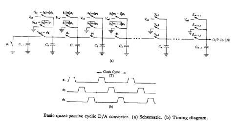
Basic Quasi-Passive Pipelined DAC
The pipelined D/A converter of Fig. 1 (a) consists of only
MOS switches and equal sized capacitors (3J. This circuit
is called Quasi-Passive (QP) since no opamp is used in
the D/A conversion process. However, an opamp may be
needed in the Sample-a,nd-Hold (S/H) circuit that follows
this DAC core.
The conversion process begins with discharging C_1
and charging Co with bo(m)Vref in ~1. By convention,
bn(m) is bit n of the digital input sample m, a.nd bo is the
LSB. In the next phase of a nonoverlapping three-phase
clock, as in Fig. 1 (b), the stored charge on Co is shared
with C_ 1 and the voltage is divided by 2 (ignoring- all
parasitic capacitors and assuming all Cns are equal for
the time being). Carrying the same analysis forward for
all other stages, and noticing the full clock cycle delays foi~
the input bits in reaching their corresponding switches,
one arrives at
N-1
YCnr-i (mJ - Yref ~ bn(m - 1~ 2n N
ri=o
which is the analog equivalent of the digital input. This
output voltage has to be sampled-and-held by a S/H
block.
Although it takes N clock phases to have a complete
conversion of a digital input sample, the conversion rate
is equal to the clock frequency, i.e. T . A special shift
r register is required to provide the proper timing for the
input bits of Fig. 1.
Stray-Insensitive Quasi-Passive Cyclic DAC
The basic CZP pipelined DAC explained in the previous
section suffers from sensitivity to stray capacitance. The
' most important stray capacitors in the circuit ase the
gate-to-cha,nnel capacitance (C~) of the MOS switches,
and the junction-to-bulk ca,pacitauce (C~) of the same
transistors. While CgB only causes offset and gain error,
l C~ causes nonlinearity in the conversion due to its voltage
dependency.
CA 02327644 2000-12-04
In the Stray Insensitive QP (SI(aP) pipelined DAC, the
operation is based on the charge stored on the sampling
capacitors only, and at the end of the conversion, the
resulting charge is transferred to a linear capacitor to
produce the output voltage. The schematic diagram of
this converter is shown in Fig. 2.
Here, a similar stray insensitive principle as in the
SIQP cyclic DAC [1] is deployed by charging the bot-
tom plate of the capacitors to bn [m] V,.ef in the sampling
phase, and permitting the the charge on the top plate
of the capacitors to participate in the conversion (charge
sharing) process.
Differential Bipolar Stray-Insensitive
Quasi-Passive Pipelined DACl
Mismatch between the identically drawn capacitors of
the pipelined DAC is caused by process imperfections
such as oxide thickness variations and inaccuracies on
the edges- These imperfections limit the matching ac-
curacy between two identically drawn 1 pF Polysilicon-
To-Polysilicon (PTP) capacitors to around 0.1% (3 times
the standard deviation). Since the matching errors are
random and (mostly) independent, the square-root of the
squared values of the individual standard deviations gives
the mismatch between the of capacitor values. Hence,
the standard deviation of the individual capacitor values
{with respect to an average value of a large number of
identically drawn capacitors on the same die) is smaller
than the standard deviation of capacitor mismatch by
a factor of ~. A simulated example of the effect of
a 240 ppm standard deviation in capacitor values of a
pipelined DAC on its DC linearity is shown in Fig. 3.
Although the pipelined DAC is less sensitive to capac-
itor mismatch than the cyclic DAC (because of an aver-
aging effect due to the large number of capacitors used),
its linearity is still limited by this factor for many ap-
plications. To alleviate this sensitivity, a similar bipolar
1 Patent pending
CA 02327644 2000-12-04
technique, as explained in (4), (5J, for the cyclic DAC can
be used.
The digital input to the bipolar DAC is in sign-
magnitude format, and its sign bit sets the polarity of
the reference voltage used in each stage. In the new ar-
chitecture, the linearity is improved by one bit, and the
(statistically) worst case nonlinearity point is moved from
the middle of the range to the 1/4 and 3/4 of the range
points, as shown in Fig. 4.
A differential architecture similar to the one used in
(4), (5) (not shown here) should be used to avoid the non-
linearity caused by reference voltage mismatch.
Sample-and-Hold
After complete conversion of a digital input sample to an
equivalent charge on the last node in the DAC pipeline
(top plate of CN_i), the resultant charge should be trans-
ferred to a linear capacitors) in order to produce a linear
output voltage. This function is performed in a S/H stage
CA 02327644 2000-12-04
following the pipeline as shown in Fig. 2. This S/H stage
is also a low-pass Infinite Impulse Response (IIR) filter.
Since the pipelined stages are made of MOS switches
and capacitors only, they settle much faster than the S/H
opamp. To avoid this bottleneck on the speed of the
converter, two last stages can be used to alternatively
participate in the D/A conversion and the charge transfer
to the S/H. The resulting multiplexed last stage, shown
in Fig. 5 in a single-ended view, can effectively triple the
conversion speed, since the sample-and-hold phase now
extends for three clock phases. Notice the use of upper-
case notation for superphases ~1 and ~2 that last for a
complete clock cycle (three phases) each.
Continuous-Time (CT) linearity of the output voltage
of the S/H stage at the output of a SIQP pipelined DAC
is compromised by the presence of nonlinear junction ca-
pacitors that are discharged by the S/H opamp. A second
S/H is needed to provide better CT linearity at the out-
put. A block diagram of the complete DAC,is shown in
Fig. 6.
The second S/H uses a similar architecture as the first
S/H (Fig.7, the optional multiplexing of sampling capac-
itors not shown). Slew-limiting resistors enhance the CT
linearity of this stage by operating the opamp in a more
CA 02327644 2000-12-04
J
linear mode.
Implementation
A complete pipelined DAC is implemented in a 0.6-~c
double-poly CMOS technology. Fig. 8 is a die photo-
graph of the test chip with 4 pipelined DACs on it. Fol-
lowing each pipelined DAC, an on-chip Continuous-Time
Reconstruction Filter (CTRCF) is used to provide better
attenuation of the signal images. The total area for each
pipelined DAC, including the CTRCF, is 1.1 mm2.
Measurement Results
x The implemented pipelined DAC was run from a sin-
CA 02327644 2000-12-04
gle 5 V power supply, and the conversion rate was set
at 17.664 MSps. The power dissipation for the DAC is
43 mW, with an additional 15 mW for the CTRCF.
Measured DC linearity plots of a typical pipelined DAC
are shown in Fig. 9. This device achieves a maximum
DNL of 1.4 LSB, and a maximum INL of 1.8 LSB to 14
bits of resolution.
The measured single-tone response of a typical
pipelined DAC is plotted in Fig. 10. Performance mea-
sures cover the bandwidth of 0 to 1.6 MHz.
The dynamic performance of the converter at higher
frequencies ca,n be evaluated by an intermodulation dis-
tortion test. The result, shown in Fig. 11, indicates third
and fifth intermodulation distortion products at -83.8 dB
and -90.8 dB below the tones respectively.
CA 02327644 2000-12-04
Conclusions
The stray-insensitive quasi-passive pipelined DAC archi-
tecture presented in this paper provides a better alterna-
tive to the traditional stray-insensitive design. The better
accuracy, lower power consumption, and smaller size of
the new design is further enchanced by the differential
bipolar method.