Note: Descriptions are shown in the official language in which they were submitted.
CA 02327709 2000-12-06
Fishman 12-19-3 1
IMPROVED DISTORTION ANALYZER FOR COMPENSATION APPARATUS
OF FIRST-ORDER POLARIZATION MODE DISPERSION (PMD)
Field Of The Invention:
The invention relates to optical transmission systems and more particularly
relates
to dealing with so-called polarization mode dispersion in such systems.
Background Of The Invention:
Polarization Mode Dispersion (PMD) occurs in an optical fiber as a result of a
small residual birefringence that is introduced in the fiber core by
asymmetric internal
stress as well as random polarization coupling due to external forces acting
upon the
1o fiber. It is well-known that PMD may severely impair the transmission of a
signal in an
optical fiber network. This is especially the case in modern digital lightwave
systems that
operate at bit rates of at least 10 Gb/s per transmitted wavelength channel.
U. S. Patent No. 5,930,414, which issued July 27, 1999 to D. A. Fishman et al,
discloses different apparatus for mitigating signal impairments due to PMD.
Such
apparatus employs a variable optical birefringence element which introduces a
differential
optical time delay between at least two selectable mutually orthogonal
polarization
states, i.e., the "Principal States of Polarization" (PSP) in the transmission
fiber. An
optical distortion analyzer coupled to the output of the variable
birefringence element
generates a control signal for that element.
2o The compensation apparatus shown in FIG. 4 of the referenced '414 patent
generates a continuously variable Differential Group Delay (DGD) between two
principal states of polarization to compensate for first-order PMD in the
transmission
fiber. One difference between this arrangement and the time-delay line shown
in FIG. 1
of the referenced '414 patent is that the PSPs of the variable birefringence
element in the
apparatus of FIG. 4 of the '414 patent is frequency dependent. Such frequency
dependence (which is an important aspect of a so-called second-order PMD
effect) may
lead to excessive distortion in the optical signal, since the first-order PMD
in the fiber
CA 02327709 2003-11-24
2
can only be compensated for over a certain optical bandwidth. Moreover, the
PMD
may even increase in certain parts of the optical spectrum.
Signal distortion caused by the second-order PMD effect in conventional
non-return-to-zero (NRZ) and return-to-zero (RZ) digital optical signals may
be
observed in the electrical spectrum of the received optical signal as a
narrowband
"tone" of spectral energy at the certain frequencies related to the signal bit
rate, e.g.,
GHz for NRZ and 20 GHz for RZ signals.
Summary Of The Invention
We decrease substantially the distortion caused by second-order PMD effects
1 o in a variable birefringence element of PMD compensation apparatus by
modifying the
control signal applied to the variable birefringence element such that the
optical signal
experiences minimal second-order PMD. In particular, the control signal
generated
by the distortion analyzer of FIG. 2 or 8 of the above-referenced '414 patent
is
modified by subtracting from the control signal in a weighted fashion the
output
t 5 signal of a bandpass filter tuned to the narrowband tone outputted by the
distortion
analyzer. The resulting modified signal, Vf, is then supplied to the
polarization
controllers in the variable birefringence element to reduce the level of the
distortion
that occurs as a result of the aforementioned second-order effect. The
modified Vf,
more particularly, causes the PMD compensator to operate at a point where the
overall second-order distortions in both the transmission fiber and PMD
compensator
are minimal. The inventive feature particularly orients the PSPs of the
compensator
to offset any second-order PMD distortion that may be generated by the
transmission
fiber. That is, the second-order effect is subtracted from, rather than added
to, the
distortion produced by the transmission fiber.
In accordance with one aspect of the present invention there is provided a
compensator for compensating for the effects of polarization mode dispersion
occurring in an optical transmission fiber having principal states of
polarization, the
compensator comprising: first means for reorienting the polarization of
particular
components of an optical signal received over the optical transmission fiber;
second
CA 02327709 2003-11-24
means for dividing a signal coupled to an output of the first means into a
predetermined number of signals each having a polarization state oriented
orthogonally to a respective one of the two principal states of polarization
and for
delaying each such divided signal a variable amount of time; and third means
for
converting a portion of a signal outputted by the apparatus into an electrical
signal and
for splitting the converted signal into a plurality of signals and supplying
the split
signals to first, second and third analyzer sections, respectively, in which
the first
section operates to pass the entire spectrum of the outputted signal, the
second section
operates to pass only that portion of the entire spectrum that is below a
predetermined
t o frequency and the third section operates to pass a predetermined band of
the entire
spectrum, and wherein said third means includes means for summing the outputs
of
the first and second sections and subtracting the output of the third section
from the
summed result to generate a distortion indicator and for supplying the
distortion
indicator to the first and second means, and wherein said first and second
means,
responsive to a change in the level of the distortion indicator, respectively
changing
until the level of the distortion indicator reaches a predetermined level, the
orientation
of each of said polarization state and said variable amount of time.
In accordance with another aspect of the present invention there is provided a
compensator for compensating for the effects of polarization mode distortion
occurring in an optical transmission fiber having principal states of
polarization, the
compensator comprising: first means for reorienting the polarization of
particular
components of an optical signal received over the optical transmission fiber;
second
means for dividing a signal coupled to an output of the first means into a
predetermined number of signals each having a polarization state oriented
2s orthogonally to a respective one of the two principal states of
polarization and for
delaying each such divided signal a variable amount of time; and receiver
means
having an optical converter for converting a portion of a signal outputted by
the
second means into a predetermined signal and generating AC and DC component
signals from the converted signal and wherein said receiver means supplies the
AC
3o component signal to a distortion analyzer that measures the level of at
least first-order
PMD distortion in the AC component and outputs a signal indicative of the
level of
CA 02327709 2003-11-24
4
such distortion and supplies the DC component to signal squaring means and
wherein
said compensator further comprises; divider means that divides the level of
the signal
indicative of said distortion by the level of the squared signal and supplies
the
resulting quotient signal as a distortion indicator to the first and second
means, and
wherein said first and second means, responsive to a change in the level of
the
distortion indicator, respectively change, until the level of the distortion
indicator
reaches a predetermined level, the orientation of each of said polarization
state and
said variable amount of time.
These and other aspects of our invention are set forth in the following
detailed
to description, corresponding drawings and ensuing claims.
Brief Description Of The Drawings
FIG. 1 illustrates in block diagram form an illustrative prior art system in
which the principles of the invention may be practiced;
FIG. 2 is a block diagram of another illustrative distortion analyzer that may
1 s be used to derive a feedback signal for the PMD compensator of FIG. 1;
FIG. 3 is a block diagram of an improved distortion analyzer; and
FIG. 4 is a block diagram of another improved distortion analyzer.
Detailed Descrij~tion
For the sake of clarity and continuity the inventive feature will be discussed
in
2o the context of the compensation system disclosed in the aforementioned U.S.
Patent
No. 5,930,414.
Polarization Mode Dispersion (PMD) occurs in single-mode fibers as a result
of residual birefringence in the fiber core and coupling of random
polarization at
various points along the fiber.
25 It is well-known that for any optical frequency, w = wo, there exist two
orthogonal states of polarization commonly referred to as the Principal States
of
CA 02327709 2003-11-24
4a
Polarization (PSP). An optical signal propagating through a fiber does not
experience any significant amount of differential time delay if it is
polarized at one of
the two PSPs.
It can be appreciated that a differential group delay, if, occurs between the
two
PSPs of the fiber. The differential group delay (DGD) which an optical signal
experiences as a result of propagating through an optical fiber may be
compensated
for by introducing an opposite but equal amount of differential time delay, i~
_ -if, at
the output of the fiber. This may be readily done using an optical element
having the
polarization characteristics disclosed in the aforementioned patent.
1 o PMD in a fiber may change with time and/or with changes in optical
frequency. A change in PMD may include changes in the corresponding PSPs as
well
as changes in DGD, if, which may be compensated for by varying the amount and
orientation of the birefringence in the compensator to adaptively compensate
for the
DGD in the fiber. An adaptive, variable-birefringence compensator may be
readily
15 realized by disposing a polarization transformer, for example, the
polarization
transformer, described in U.S. Patent No. 5,212,743 issued May 18, 1993 to
F. L. Heismann, in series with an element that generates variable linear
birefringence.
Such variable birefringence may be generated by splitting the signal at the
output of
the polarization transformer into two orthogonal linear polarization states
2o corresponding to the two PSPs of the fiber, and delaying one of the two
polarization
states by a variable amount of time, i~ using a respective time delay line 50
(such as,
for example, the polarization mode dispersion emulator, model PE3 available
from
JDS Fitel Inc.) as shown in FIG. 1 of the above referenced '414 patent.
Another way of generating such birefringence is illustrated in FIG. 1. This
25 embodiment includes two nearly identical sections of high birefringence
single-mode
fibers 435 and 445 which generate fixed differential time delays, il and i2,
respectively between light signals polarized along the slow and fast optical
axis of the
two fibers. (Fibers 435 and 445 may be, for example, the SM15-P-8/125 fiber
available from Fujikura Co., having a time delay of about 1.4 ps/m). A second
3o polarization transformer 440 inserted between fibers 435 and 445
effectively controls
CA 02327709 2003-11-24
4b
the angle, 9~, between the fast axis of fiber 43S and fiber 445. The resulting
differential time delay, i~, generated by fibers 43S and 44S may be expressed
as
follows:
~ z z
~~ - 11 't ~ + 't z + 2 Z'~ Zz cos(29z )
which is continuously variable between a minimum value of ~ il - i2 ~ and a
maximum value of (il + iz).
If the polarization transformation generated in polarization transformer 430
and the differential time delay generated by fibers 43S and 44S and
polarization
transformer
CA 02327709 2000-12-06
Fishman 12-19-3
440 are properly adjusted in the manner described in the aforementioned '414
patent,
then a signal outputted by compensator 425 will be free of the distortions
caused by
differential group delays occurring in transmission fiber 420.
A feedback signal is used to control the polarization transformation in
polarization transformer 430 (i.e., the orientation of the variable
birefringence) as well as
the variable differential time delay generated by the two high birefringence
fibers 435 and
445 and polarization transformer 440. The desired feedback signal may be
generated at
the output of compensator 425 by monitoring the amount of pulse distortion
that is due
to the differential time delay present in an optical signal after it has
traveled through
1o compensator 425.
Note that only one feedback signal 471 is needed to simultaneously adjust the
polarization transformation and adjust the differential delay, i~, to achieve
minimal
distortion in the signal that compensator 425 outputs to optical receiver 490
via
conventional signal tap 485, as is shown in FIG. 1 and as will be discussed
below.
Specifically, a portion of the signal that compensator 425 outputs is supplied
via
optical tap 485 to path 487 extending to high-speed photodetector 455, which
may be,
for example the Hewlett Packard Co., model 11982 Wideband Lightwave Converter
having an electrical bandwidth that is at least equal to the information
bandwidth of the
modulated optical signal transmitted by optical transmitter 410. The remainder
of the
2o signal is supplied to path 486 extending to receiver 490. Photodetector 455
converts the
high-speed digital information signal that was modulated onto an optical
carrier signal
into an electrical signal. The electrical signal is then amplified by
conventional amplifier
460 and coupled to electrical distortion analyzer 470, which measures the
distortion in
the amplified photocurrent and converts the amplified result into a voltage,
Vf supplied
to path 471, that is proportiona: to the distortion. For example, voltage Vf
reaches a
maximum value when the optical signal is free of distortion due to first order
P1V>D, i.e.,
when the combined differential time delay of optical fiber 420 and compensator
425 is
substantially equal to zero.
CA 02327709 2000-12-06
Fishman 12-19-3 6
If the DGD in the transmission fiber is limited to values below a maximum
value,
z",ax, then the distortion in the optical signal may be quantified by simply
measuring the
amplitude of the received electrical signal of a particular frequency f <_
1/(2z~"aX). The
amplitude of this signal may then be used as a feedback signal to
automatically adjust the
orientation and level of DGD that is generated in PMD compensator 425, such
that the
feedback signal is maximized.
The above requirement set for the total DGD that may be inserted in a
transmission system, 'L~oy <_ "Cma,~, may limit the amount of DGD that may be
compensated
for in an optical transmission fiber, if, as ito,~, < 2if. For example, if in
a 10 Gbps digital
1U transmission system, the amplitude of the received electrical signal is
measured at 5 GHz,
then if should always be smaller that 50 ps. Otherwise, the feedback signal
that is
generated as a function of the amplitude of the 5 GHz component may be
ambiguous in
the sense that it is difficult to determine by which amount and direction the
polarization
transformation and the differential time delay, z~, need to be adjusted to
obtain a atom =
0, which may occur, for example, when the amplitude of the feedback signal is
the same
for two different values of ito,~,, and which may result in generating faulty
adjustments in
the orientation and level of the differential time delay in PMD compensator
425.
An "unambiguous" feedback signal (i.e., a signal that is a unique measure of
i~o,~,)
may be generated , without limiting the level of compensation that may be
applied to
2o DGD, by measuring the amplitude of a plurality of frequency components
contained in
the optical information signal propagating through an optical fiber. An
illustrative
embodiment of a compensator, which analyzes the amplitudes of substantially
the entire
received electrical frequency spectrum using a broadband electrical power
detector, is
shown in FIG. I . The broadband electrical power detector 495, which may be,
for
example, model 8474 diode detector available from the Hewlett Packard Co.,
more
particularly, converts such amplitudes into a single feedback voltage, Vf,
that is
proportional to the integral of the amplitudes (power levels) of substantially
the entire
high-frequency electrical spectrum.
CA 02327709 2000-12-06
Fishman 12-19-3 7
As mentioned above, the compensation arrangement illustrated in FIG. I
generates a continuously variable Differential Group Delay (DGD) to compensate
for
first-order DGD. As also mentioned above, one difference between this
compensation
arrangement and the differential time-delay line shown in FIG. I of the
aforementioned
U. S. Patent No. 5,930,414 is that the compensation section formed by high-
birefringence fibers 435 and 445 and polarization transformer 440 of FIG. 1
herein
exhibit Principal States of Polarization (PSPs) that vary strongly with
optical frequency.
Such frequency dependence (which is one aspect of a so-called second-order PMD
effect) may distort the optical signal in the compensator, since the DGD
experienced in
1o the fiber can only be removed over a certain optical frequency range.
Moreover, the
DGD may even increase in certain parts of the spectrum.
We have found that for conventional intensity-modulated optical signals, the
second-order PMD effect may be observed in the electrical domain by the
appearance of
a narrowband "tone" of spectral energy at the corresponding frequency of the
signal bit
rate, i.e., around 10 GHz for non-return-to-zero (NRZ) formatted digital
signals at a bit
rate 10 Gb/s and at 20 GHz for return-to-zero formatted signals at 10 Gb/s.
Thus, the
distortion caused by this second-order PMD effect may be observed using a
distortion
analyzer with an electrical filter of the type shown in FIGS. 2 and 8 of the
above
referenced '414 patent modified to have a bandpass characteristic at the bit-
rate
2o frequency.
We have further found that the effects of distortion caused by second-order
PMD
may be dealt with by subtracting in a weighted fashion the output of a
bandpass filter
tuned to the narrowband tone from the signal outputted by the distortion
analyzer of
FIG. 2 (herein). The resulting modified signal, Vf, is then supplied to the
compensator to
reduce the level of the distortion that occurs as a result of the
aforementioned second
order PMD effect. The modified Vf, more particularly, causes the compensator
to move
to (dither) a point that centers the region of correct DGD and PSP alignment
on the
spectral region of maximal distortion in the optical signal, thereby reducing
the effects of
second-order PMD. The inventive enhancement also orients the PSPs of the
CA 02327709 2000-12-06
Fishman 12-19-3 8
compensator to offset any second-order PMD distortion that a signal may
experience in
the transmission fiber in such way that the second-order PMD generated in the
compensator is subtracted from, rather than added to, the second-order PMD
distortion
experienced in the transmission fiber.
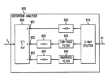
FIG. 3 shows one illustrative embodiment of a modified distortion analyzer
that
generates the aforementioned modified control signal Vf in which amplifier 460
supplies
an amplified electrical signal to the distortion analyzer, as mentioned above.
Conventional 3-way splitter 810 splits the amplified signal into three signals
that are
respectively supplied to broadband power detector 820, low-pass filter 825 and
bandpass
1o filter 840. Detector 820 in a conventional manner passes a signal (e.g., a
voltage level
proportional to the power in the entire frequency spectrum of the signal) to
adder port
851 of conventional summing circuit 850. Low-pass filter 825, on the other
hand, filters
the electrical signal allowing only that portion of the frequency spectrum
below, e.g., 2.5
GHz, to pass through to detector 830. The signal exiting detector 830 is then
presented
1s to adder port 8s2 of summing circuit 850. Bandpass filter 840, more
particularly, filters
the signal that it receives from 3-way sputter 810 and passes only those
signals within a
predetermined spectrum of signals, e.g., a one GHz band centered about 10 GHz.
The
signal exiting filter 840 is then supplied via detector 845 to negative port
853 of
summing circuit 850. Summing circuit 850, in a conventional manner, subtracts
the
2o signal that it receives via port 853 from the sum of the signals that it
receives via ports
8s 1 and 8s2. The distortion analyzer thus outputs a feedback signal, Vf,
which
negatively emphasizes the spectrum around the predetermined spectrum of
signals, e.g.,
around 10 GHz. Such emphasis causes the compensator, e.g. compensator 425 of
FIG.
1, to adapt in the aforementioned dithered manner to substantially eliminate
the
2s frequency tones that occur as a result of the second-order PMD effect, all
in accordance
with an aspect of the invention.
The feedback voltage, VF, expressed by equation (9) shown in the
aforementioned Patent No. 5,930,414 as well as the modified feedback voltage,
Vf,
generated by the distortion analyzer of FIG. 3, may be reduced by the presence
of
CA 02327709 2000-12-06
Fishman 12-19-3 9
polarization-dependent loss (PDL) that is generated in PMD compensator 425
(e.g., in
the polarization transformers). The feedback voltage, Vf, is derived from two
stages of
square-law detection (i.e., optical-to-RF, and RF-to-low frequency), and,
therefore, is
proportional to the square of the total received optical power. We have
recognized that
dividing the feedback voltage by the square of the average optical power
received by
photodetector 455 decreases substantially the adverse effects of polarization-
dependent
loss in compensator 425 and, therefore, creates a higher level of PNfD
compensation.
Such precision may be achieved, in accordance with an aspect of the invention,
by using the illustrative circuit arrangement shown in FIG. 4, in which
frequency splitter
1005 in a conventional manner separates the electrical signal outputted by
high-speed
photodetector 455 (also shown in FIG. 1) into high-frequency (AC) and low-
frequency
(DC) components. In an illustrative embodiment of the invention, sputter 1005
may be
formed from, for example, one or more conventional transimpedance LC circuits.
The
high frequency components, which contain information relating to the
distortion in the
high-speed digital signals are, after optional amplification, supplied to
distortion analyzer
1010, which may be, for example, either the distortion analyzer of FIG. 2 or
3. The low
frequency (DC) components, having levels proportional to the average received
optical
power, are supplied to conventional analog squaring circuit 1020. (In an
illustrative
embodiment of the invention, squarer 1020 may be, for example, an analog
multiplier
2o having two inputs connected together.) The signal at the output of squarer
1020 is then
supplied to the denominator terminal, D, of conventional analog divider 1030.
The
feedback voltage, Vfo, from distortion analyzer 1010 is supplied to the
numerator
terminal (N) of divider circuit 1030. The resultant quotient is then supplied
at the output
of divider 1030 as the feedback signal, Vf, which has been normalized by the
received
optical power to remove the effects of optical power fluctuations due to PDL.
A reduction in response to undesired polarization-dependent-loss effects that
occur in PMD compensator 425, and a reduction in the required dynamic range of
the
control circuitry for the automatic polarization transformers are among the
advantages
obtained from the inventive features described above.
CA 02327709 2000-12-06
Fishman 12-19-3 10
The foregoing is merely illustrative of the principles of the invention. Those
skilled in the art will be able to devise numerous arrangements, which,
although not
explicitly shown or described herein, nevertheless embody those principles
that are
within the spirit and scope of the invention. For example, based on the
foregoing, it
would be obvious to the skilled practitioner that the effects of still higher-
orders of PMD
may be dealt with by merely expanding the compensator, e.g., compensator 425,
to
include additional sections of high-birefringence fibers and polarization
transformers, as
needed.