Note: Descriptions are shown in the official language in which they were submitted.
CA 02327710 2000-10-OS
WO 99/53732 PCT/US99/08432
Dual-Use Electronic Transceiver Set for Wireless Data Networks
Field of the Invention
The present invention relates to the simultaneous dual use of radiation, e.g.
visible light, for both a conventional application, e.g., illumination,
combined with the
additional application of transmitting information without wires. The present
invention
further relates to electronic ballast circuits for electric discharge lamps,
e.g.,
fluorescent lamps. The present invention further relates to the application of
a time-
varying, modulated current through the lamp to produce electronically
detectable
~~ariations in the lamp light that are invisible to the human eye. The present
invention
further relates to coding information in variations in the lamp light for
purposes of
transmitting all kinds of information, including, but not limited to, digital
data, audio,
textual, and graphical signals. The present invention further relates to
efficient coding
schemes to maximize the bandwidth or information transfer capability of the
optical
data channel. Wide bandwidth and efficiency are critical for intranets or
other wide
area networks that could be carried on the lighting in an office or factory.
The present
invention further relates to efficient power electronic circuits capable of
producing
modulated currents in a lamp with high power efficiency, maximum data rate,
and the
possibility of incorporating needed safety features such as galvanic
isolation. The
present invention further relates to the construction of receivers for
detection of the
modulated information in the lamp light.
Background of the Invention
Over half of the artificial light produced in the United States comes from
lamps in which an electric discharge through a gas is used to produce
illumination
(J. Waymouth, Electric Discharge Lamps, MIT Press, Cambridge, Massachusetts,
3o 1971). The prevalence of electric discharge (e.g., fluorescent)
illumination has led
us to develop ways to inexpensively use discharge lamps for communication.
The basic idea of using lighting to send information as well as to provide
illumination appears to have originated at least as early as 1975 (M. Dachs,
'Optical Communication System," U. S. Patent #3900404, August 1975). In the
CA 02327710 2000-10-OS
WO 99/53732 PCT/US99/08432
Dachs patent, the inventor discloses an analog amplitude-modulation (AM)
scheme
to modulate the arc current in a fluorescent lamp, the "carner" signal, with
an
audio information signal. A more recent patent {K. King, R. Zawislak, and R.
Vokoun; "Boost-Mode Energization and Modulation Circuit for an Arc Lamp,"
U. S. Patent #5550434, August 1996) discloses an updated electronic circuit
that
also provides for AM modulation of the arc current with an analog signal. Such
techniques are generally undesirable for the direct transmission of data
since,
among other reasons, low frequency content in the data may lead to perceptible
flicker in the light output, and the noise immunity of the overall transceiver
system
is not optimal. Techniques for encoding digital information have been
described in
M. Smith, "Modulation and Coding for Transmission using Fluorescent Lamp
Tubes, "U. S. Patent #5657145, August 1997 and T. Gray, "Transmission System,
" U. S. Patent #5635915, June 1997 which employed either a pulsed AM or a
phase
modulation technique, respectively. Both techniques transmitted data at a rate
that
is on the same order of magnitude as that of the power-line frequency (50/60
Hz),
i.e., relatively slowly compared to typical modern lamp arc frequencies in the
range
of 20,000 to 40,000 Hertz. Other communication schemes have also been proposed
that do not use the lamp light as the carrier, but instead use the lamp
fixture as an
antenna for transmitting conventional radio wave or microwave signals. In K.
2o L~ehara and K. Kagoshima, "Transceiver for Wireless In-Building
Communication
Swem [sic]," U. S. Patent#5424859, June 1995, for example, the inventors
disclose
techniques for mounting a microwave antenna on the glass surface of
fluorescent
and incandescent lamps.
In T. Buffaloe, D. Jackson, S. Leeb, M. Schlecht, and R. Leeb, "Fiat Lux:
A Fluorescent Lamp Transceiver," Applied Power Electronics Conference,
Atlanta,
Georgia, June 1997, the authors outlined the possibility of using pulse-code
modulation to transmit data with a fluorescent lamp. This scheme made use of a
tri-level pulse coding, which led to a ballast design with a relatively high-
complexity compared to the architectures described in the present invention.
Also,
the associated receiver was more complicated, and unable to support the high
data
rates achievable with the present invention.
We have invented a communication network based on frequency modulated
2
CA 02327710 2000-10-OS
WO 99/53732 PCT/US99/08432
radiation (e.g., visible light) that eliminates the disadvantages of the
systems in the
prior art. It enables higher power commercial scale lighting systems to be
used to
transmit the signal. It eliminates undesirable visual flicker in the system
and so
allows simultaneous continuous use of the lighting fixtures as lighting while
also
providing the medium for communication. It allows analog, digital or
analog/digital data to be sent and received. It increases the bandwidth
available to
transmit data, and it enables a number of applications, such as multiple
digital data
streams, to be performed using a single lamp. Improvements made in the current
invention can result in unprecedented performance advantages in the operation
and
implementation of lamp transceiver systems.
This invention is the first to propose establishing a transceiver system using
any radiating transmitter with dual utility where the primary utility is any
application, not just illumination but also possibly range finding, lane
marking, or
other applications, and the secondary utility is communication. This invention
is
the first to propose the transmission of bandlimited analog information such
as
audio signals by using frequency modulation, which enhances the noise immunity
and available bandwidth over previous schemes while specifically avoiding
sensory
perceptible flicker in the transmission. It is the first to propose the
efficient
transmission of digital data using pulse code frequency modulation, and also
the
2o first to propose encoding digital bits in sidebands around the carrier
frequency of
the transmitter. It is the first to propose the use of a nonlinear detector in
a dual-
use network receiver to improve settling and detection time of pulse-coded
data.
These schemes for the transmission and reception of digital data substantially
enhance the available data transmission rate in comparison to schemes in the
prior
art, again while elimination perceptible flicker. It is the first to disclose
schemes
for creating multiple data transmission channels using the same transmitter,
and the
first to propose a receiver in a "dual-use" network capable of selecting one
channel
from a spectrum of available choices. It is the first to propose a receiver
with
variable "lock-in" or transmitter capture characteristics, allowing the
tailoring of the
behavior of the receiver as it locks on to different transmitters. This
feature could
be especially important for optimizing the receiver's behavior in way-finding
applications, and in environments with many different closely spaced
transmitters,
3
CA 02327710 2000-10-OS
WO 99/53732 PCT/US99/08432
to ease the process of acquiring and holding a data channel between the
transmitter
and receiver.
Summary of the Invention
In one aspect, the invention is apparatus for generating electromagnetic
radiation in which the radiation has both a first and a second utility. The
electromagnetic radiation is modulated to produce electronically detectable
variations to achieve the second utility, the variations not affecting the
first utility.
In one embodiment, the second utility is transmission of information. In this
embodiment, the electromagnetic radiation is visible light in which the first
utility
is illumination and the second utility is the sending of information, the
variations in
the visible light being invisible to the human eye. Suitable apparatus is a
lamp
which may, for example, be a fluorescent, cold cathode or a high-intensity
discharge lamp. Any transmitter of radiated energy could be used, however,
including light emitting diodes, lasers or radio wave antennas.
In another aspect, the invention is a lamp for generating visible light to
provide illumination and to transmit information to a receiver in which the
variations in the light as a result of the information transmission are
undetectable to
the human eye. The lamp includes a source of visible light and circuitry
including
a ballast for modulating the output of the source to send information by means
selected from the group including analog FM, sideband encoded digital pulse
code
FM, discrete pulse code FM with two level coding, and any other orthogonal bit
coding scheme. The circuitry may further include a rectifier for drawing power
from an AC source and controlling the power to have substantially the same
shape
and phase, but possibly different amplitude, as the AC source to insure near-
unity-
power-factor operation. An inverter is connected to receive power from the
rectifier to create a high frequency alternating wave form, the output of the
inverter
forming an input to the lamp. It is preferred that the inverter include means
for
varying the frequency of the voltage produced by the inverter. It is also
preferred
that the inverter is operated with zero-voltage or zero current switching.
In particular, the present invention pertains, in part, to electronic circuits
capable of controlling and modulating the arc current in a lamp. The circuits
4
CA 02327710 2000-10-OS
WO 99/53732 PCT/US99/08432
include means to draw power from a direct or alternating (utility) source. The
circuits further include means to control or limit the magnitude of the
current
flowing in a lamp or collection of lamps. The circuits further include means
to
vary the current in the lamp to encode information in the lamp light with no
visible
flicker.
By "lamp", as that term is used herein, it is meant a device that produces
radiated transmissions, including, but not limited to, infra-red, visible, and
ultra-
violet light, in response to an input electrical current which flows in the
lamp. A
typical example is a fluorescent lamp, although other types, such as high-
intensity
discharge lamps, light emitting diodes, lasers, cathode ray tubes, particle
beam
emitters, liquid crystal displays, electroluminescent panels, klystrons, and
masers
are also intended. Emitters of other types of radiation, such as radio
antennae for
applications in RADAR sets, ultrasonic transducers, and mechanical fans
("radiating" air or water for instance) are also intended.
By "ballast", as that term is used herein, it is meant a circuit that controls
the amplitude, frequency, and phase of the current waveform in the lamp.
By "rectifier", as used herein, it is meant a circuit that takes as input a
voltage
waveform from a power source and produces a DC or predominantly DC output
voltage waveform.
By "inverter", as used herein, it is meant a circuit that takes as input a low
frequency or DC electrical voltage waveform from a power source. The inverter
produces a high frequency voltage waveform that can be applied to the lamp. or
a
lamp in combination with other electrical components such as inductors or
capacitors. The frequency and phase of this output voltage waveform can be
controlled by the inverter.
By "switch", as used herein, it is meant a device that can either block or
permit the flow of electric current in response to a low-power-level control
signal.
Typical examples of a switch include a bipolar junction transistor, a MOSFET,
or
an insulated-gate bipolar junction transistor (IGBT).
By "load", as used herein, it is meant a lamp or lamps, possibly in
combination with other electrical components including inductors, capacitors,
resistors, and transformers, which are added to ensure that proper and safe
5
CA 02327710 2000-10-OS
WO 99/53732 PCT/US99/08432
operating voltages and currents are, or can be by virtue of control actions
taken by
the inverter, applied to the lamp or lamps. Typically, the load is connected
to the
output of an inverter.
In one embodiment of the invention, a system that is capable of controlling
the
current in a discharge or fluorescent lamp is provided. A rectifier circuit is
used to
draw power from the AC utility. The current drawn from the AC utility by the
rectifier circuit is actively controlled to have the same shape and phase, but
possibly a different amplitude, as the AC utility voltage waveform, ensuring
near-
unity-power-factor operation. The power drawn from the AC utility is used to
create a predominantly DC output voltage with little alternating or ripple
voltage.
This DC voltage serves as the input to an inverter circuit.
The inverter circuit draws power from the DC bus and creates a high
frequency alternating waveform that can be applied to the lamp, or the lamp in
combination with other electrical components including transformers,
inductors, or
capacitors. For example, the inverter can be used to apply an AC square wave
to
the primary of a transformer whose secondary is cormected to a series
combination
of an inductor and a capacitor and lamp in parallel. The inverter circuit
includes
special means to vary the frequency of the voltage produced by the inverter
circuit.
The frequency can, for example, be varied to encode information in the output
voltage waveform and, therefore, the light produced by the lamp. To maximize
efficiency, the inverter is operated with zero-voltage switching. For example,
switches are turned on only when the voltage across the switch is zero,
ensuring a
nearly lossless turn-on transition.
In another embodiment, the inverter circuit could be energized directly by a
DC or low frequency alternating power source, eliminating the need for a
rectifier
circuit. This mode of operation is particularly attractive in environments,
e.g.,
automobiles or other transportation systems, where DC power is available a
priori.
Again, the inverter circuit includes special means to vary the frequency of
the
voltage produced by the inverter circuit. The frequency can, for example, be
varied to encode information in the output voltage waveform and, therefore.
the
light produced by the lamp. Again, to maximize efficiency, the inverter is
operated
with zero-voltage switching. For example, switches are turned on only when the
6
CA 02327710 2000-10-OS
WO 99/53732 PCT/US99/08432
voltage across the switch is zero, ensuring a nearly lossless turn-on
transition.
In either case, a receiver can be constructed which remotely samples the
lamp light from a distance and decodes the information in the light encoded by
the
ballast.
Brief Description of the Drawings
The invention will be understood with reference to the drawings, in which:
FIG. 1 is a schematic illustration of the system of the invention.
FIG. 2 is an electronic schematic diagram of a high frequency half bridge
inverter
which may be used to drive a load.
FIGS. 3a and 3b show oscilloscope traces of the gate drive and switch voltage
waveforms in an inverter operated with zero-voltage switching (ZVS).
FIG. 4 is an electronic schematic diagram of a high frequency half bridge
inverter
driving the primary of a center-tapped transformer whose secondary may be used
to
drive a load.
FIG. 5 is an electronic schematic diagram of a high frequency full-bridge
inverter
which may be used to drive a load.
FIGS. 6a, 6b and 6c are schematic diagrams of possible load configurations.
FIGS. 7a, 7b and 7c are schematic diagrams of three possible modulation
circuits
for modifying the operating frequency of the inverter circuit.
FIG. 8 is a graphical representation of a half weight bit pattern.
3o FIGS. 9a and 9b are graphs showing a spectrum comparison illustrating the
advantage of half weight bit coding.
7
CA 02327710 2000-10-OS
WO 99153732 PCT/US99/08432
FIG. 10 is a block diagram illustrating a receiver architecture for decoding
digital
data transmitted by the light.
FIGS. l la and llb are graphs that show a comparison of sent and received
encoded bits respectively in a prototype system.
FIG. 12 is a block diagram showing a finite-state machine that could be used
to
encode digital data transmission through the modulation circuits.
Detailed Description of the Invention
The present invention transmits information over a free space optical data
pathway. Transmission is accomplished by modulating or varying the frequency
of
the alternating current in an electric discharge lamp such as a fluorescent
lamp. A
typical discharge lamp requires a relatively high starting or striking voltage
across
it's terminals to form an arc or electric discharge in the lamp. Once the arc
forms,
it is essential to reduce the voltage across the lamp, lest an excessive
current flow
through the lit lamp, destroying it. The purpose of an electronic lamp ballast
is at
least two-fold, therefore. The ballast must provide an adequately high voltage
to
initiate arc formation and light production. After starting, the ballast
serves to limit
the current through the lamp, ensuring satisfactory light production and long
lamp
life. The present invention adds a third function to the ballast. A means is
provided to vary the frequency of the lamp current to encode information for
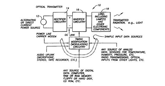
transmission in the lamp light. An overview of this new ballast is shown in
Figure 1. Ballast 10 draws power from an alternating or direct current
electric
power source 12. This power is processed by a rectifier pre-regulator circuit
14,
which may perform several functions, including actively wave-shaping the input
current to provide near-unity-power factor operation. The rectifier 14 also
provides
a DC output voltage or DC link that serves as the input to the next stage in
the
ballast 10, an inverter 16. It should be noted that there are a wide range of
possibilities for implementing this rectifier stage, including actively
controlled pre-
regulator circuits designed around well known power electronic switching power
supplies such as the buck, boost, or flyback converters (not shown). This
stage
8
CA 02327710 2000-10-OS
WO 99/53732 PCT/US99/08432
might or might not provide safety isolation by incorporating a transformer, as
needed. It might also be a very simple stage, consisting of as little as a
capacitor
or simply a pair of connecting wires if the ballast is to operate from a DC
source
voltage, as might be the case in a transportation system such as an automobile
or
bus, where a 12 volt DC supply may be conveniently available, for example.
The inverter circuit 16 operates from the DC link voltage provided by the
rectifier 14. The inverter 16 acts to create a high-frequency AC voltage
waveform
to be applied to a load circuit 18 that includes one or more lamps. There are
a
tremendous number of inverter circuit topologies and switching schemes that
could
be used for this application. One possibility, for example, is shown in Figure
2. A
half bridge inverter 20 shown in the figure consists of two IRF840 MOSFETs 22
and two capacitors that divide the DC link voltage, Vd~. A control circuit 26
acts to
activate first the bottom MOSFET, and then the top MOSFET, and then repeats
this pattern. One complete cycle of the pattern will be called a switch
period. A
wide range of chips or circuits could be used to control the two MOSFETs in
the
inverter 20. One possibility, for example, would be to use the IRF2155 half
bridge
control circuit 26, which contains drivers for the MOSFETs and a built in
timing
circuit to determine the time interval that constitutes a switch period. This
interval
can be controlled by the ballast designer in the case of the IR2155 control
chip by
selecting the values of the resistor Rt 28 and the capacitor Ct 30. A critical
innovation in the present invention is the addition of modulation circuitry 32
to
modify the behavior of the timing circuitry to permit frequency modulation of
the
inverter AC waveform for the purpose of encoding information for transmission
at
the highest possible bandwidth or data rate while ensuring that the lamp 34
light
exhibits no perceptible flicker regardless of the information content of the
ttzrnsmitted data. This information could come from any source of analog or
digital waveforms, as shown in Figure 1, including, for example, audio signals
from a tape recorder or microphone or digital data from a computer, disk
drive, or
power line earner modem.
The inverter block 16 shown in Fig. 1, and illustrated as a half bridge
circuit 20 in Figure 2, is used to drive a load circuit that consists of the
lamp 34
and possibly other electronic elements such as inductors, capacitors, and/or
9
CA 02327710 2000-10-OS
WO 99/53732 PCT/US99/08432
transformers. A specific example is shown in Figure 2, in which the load
consists
of a transformer 36 driving a series combination of an inductor 38 and the
parallel
combination of a capacitor 40 and the lamp 34. The transformer 36 can provide
at
least two important functions. It may provide galvanic safety isolation,
especially
if the rectifier circuit 14 that provides Vd~ does not incorporate means for
isolating
the circuit. It may also provide a change in the voltage level from the
primary
winding (driven by the inverter) to the secondary winding (connected to the
inductor, capacitor, and lamp) in order, for instance, to enhance available
striking
voltage. The inductor 38 and capacitor 40 in this load serve as a high-Q
resonant
circuit when the lamp 34 is off, i.e., before the arc strikes, which can also
provide
significant striking voltage if the inverter frequency is near the resonant
frequency.
Once the lamp 34 strikes, the lamp 34 effectively dominates the combined
impedance of the capacitor/lamp pair, and the inductor serves to limit the
current
flowing through the lamp in steady-state operation.
The two MOSFETs 22 in the inverter must never be turned on
simultaneously, in order to avoid short circuiting the input voltage Vd~. If a
delay
is left by the control circuit between the time that one switch is turned off
and the
next switch is turned on, it is possible to operate the inverter with highly
efficient,
zero-voltage switched turn on transitions. This is illustrated in our
experimental
prototype by the waveforms shown in Figs. 3a and 3b. The top oscilloscope
photo
of Fig. 3a shows the delay between the activation signal for the top MOSFET
and
the bottom MOSFET. The bottom oscilloscope photo of Fig. 3b shows that the
drain-to-source voltage on the bottom MOSFET, for example, rings to zero volts
and is clamped by the MOSFET body diode before the bottom MOSFET is turned
on by its control signal. In the half bridge inverter, ZVS is ensured by
leaving a
delay between the switch activations and by ensuring that the inductor 38 is
large
enough to store sufficient energy to ring the drain-to-source voltage to zero.
Two of an innumerable number of possible configurations for an inverter
circuit are shown in Figures 4 and 5. In Figure 4, an inverter 42 has been
modified to include a center-tapped transformer 44. This configuration has the
advantage of allowing both MOSFET control gates 22 to be driven with respect
to
around. However, it also raises the complexity of the transformer
manufacturing
CA 02327710 2000-10-OS
WO 99/53732 PCT/US99/08432
by requiring a center-tapped primary. In Figure 5, an inverter 46 has been
modified to be a full-bridge, four switch inverter. This circuit has the
advantage of
applying the full voltage Vd~, as opposed to Vd~/2 in the half bridge, making
it
potentially easier to develop a high striking voltage. However, it also
requires four
switches and possibly four control lines from the control circuitry.
These inverter configurations all typically drive the load with a
predominantly sinusoidal arc current. Other inverter configurations could be
used,
at the risk of increasing the lamp current crest factor, to drive a current
consisting
of the sum of two or more distinct carrier frequency sinusoids. Each of these
sinewaves could be modulated with a different information signal, enabling the
possibility of using a single lamp to send multiple channels of information,
for
which a receiver could individually tune and detect.
Three different example load configurations, again from an almost
innumerable number of variations, are illustrated in Figs. 6a, 6b and 6c. In
each of
the three cases, it is assumed that the load is driven by the high frequency
output of
some inverter circuit. The load configuration in Figure 6a illustrates the use
of a
single transformer 36 to drive multiple L-C-Lamp circuits 48,50, permitting a
multi-lamp fixture and ballast. The load circuit of Fig. 6b also permits the
operation of multiple lamps 34,52 by connecting the lamps in series. This
configuration minimizes the need for additional inductors and capacitors, but
requires a high transformer turns ratio and/or high-Q L-C circuit to provide
the
high striking voltage needed to activate a series combination of lamps. Also,
in
this configuration, if a single lamp fails, the entire fixture (both lamps
34,52 in the
figure, for example) will cease to produce light. The third circuit shown in
Fig. 6c
can be used to activate one or more lamps in parallel. The capacitors 54 serve
as
ballasting or current limiting elements, and striking voltage is provided by a
transformer with a sufficient turns ratio to provide high voltage to the
lamp/capacitor combinations. This configuration requires a transformer 36 with
a
high turns ratio, and has the advantage that the failure of one lamp will
generally
3o not interfere with the operation of the other, parallel lamp circuits. Note
that other
enhancements, such as the addition of a positive-temperature coefficient
thermistor
(not shown) in parallel with each lamp, might be made in any of the load
11
CA 02327710 2000-10-OS
WO 99/53732 PCT/US99/08432
configurations to enhance starting and prolong cathode life.
In a multi-lamp fixture, notice that several configurations are possible. As
shown in Figs. 6a, 6b and 6c, several loads could be connected to the same
inverter, increasing the total radiated power of a particular signal. It is
understood,
however, that individual lamps in a mufti-lamp fixture could be connected to
one of
several inverter circuits with different modulation inputs. In this case, a
single
lighting fixture could be used to transmit data on multiple channels.
At the heart of the invention is some circuit means to enable frequency
modulation or pulse code frequency modulation of the lamp 34 light. For
purposes
of illustration, it is assumed that the switch period is determined by the
action of a
hysteresis oscillator, as is found in the IR2155 or the classic 555 timer
circuit. A
hysteresis comparator or set of comparators is included in the control chip or
circuitry. The switch period is normally set by this comparator and the values
of
Rt and Ct, which work together to create an oscillator. In the present
invention, the
timing circuit 32 is modified to permit analog frequency modulation (FM) or
digital
pulse code modulation of the inverter timing, and therefore the lamp current.
It
should be understood that a wide range of possibilities exist for determining
the
timing of a switch period and the pattern of switch activation in the
inverter. Any
timing circuit that permits frequency modulation or digital pulse code
modulation
(W.M. Siebert, Circuits, Signals, and Systems,McGraw--Hill, New York, New
York, 1986), e.g., with half weight block codes, does not depart from the
spirit or
scope of the invention.
For illustration purposes, three different modulation circuits designed to
modulate the behavior of the hysteresis oscillator are shown in Figs. 7a, 7b
and 7c.
In the first design of Fig. 7a, the signal to be transmitted over the lamp
light, e.g.,
an analog audio signal from a tape recorder or microphone, is received through
an
audio transformer 60 which can provide both voltage level conversion and
safety
isolation. The AC audio signal at the secondary of the transformer 60 is level-
shifted by the action of a potentiometer 72 to create a signal which consists
of an
3o AC signal with a DC offset, ensuring that the voltage applied to R with
respect to
ground is always non-negative. The impedance of the potentiometer 72 should be
low, i.e., on the order of the impedance of the transformer 60
secondary~winding or
12
CA 02327710 2000-10-OS
WO 99/53732 PCT/US99/08432
smaller. Also, the resistance of the transformer 60 secondary winding should
be
large enough (e.g., 600 Ohms or more) to limit the current flowing out of the
transformer, thus avoiding magnetic saturation. The filter formed by R and C
serves to limit the high frequency content of the input signal. The breakpoint
of
this filter can be varied by changing the values of R and C to vary the
bandwidth
or baud rate of the transmitter. In our prototype, for example, R was
eliminated
entirely, leaving just the filtering provided by C and the transformer
secondary
impedance. The voltage level on the capacitor C varies slowly with respect to
the
switch frequency (e.g., half the switch frequency or less). This voltage level
couples to the action of the hysteresis oscillator through two diodes 74 and a
series
capacitor 76. It alters the trigger point of the oscillator, permitting the
voltage on C
to frequency modulate the oscillator and therefore the inverter. In summary,
the
level of the slowly varying AC input voltage on the transformer primary
ultimately
frequency modulates the inverter and the current in the load and lamp.
The circuit in Figure 7b can also modulate the inverter by similar means.
In this case, however, the input signal is presented through an optoisolator
78
instead of a transformer. This design might be most suitable for discrete
input
data, i.e., data which assumed specific levels such as a digital waveform.
However,
with the optoisolator 78 with reasonably linear response, this design could
also be
used to transmit analog signals. Note that if isolation is not necessary, the
input
vraveform could be applied directly to the RC filter.
The circuit in Figure 7c can also be used to modulate the inverter. In this
case, the AC input waveform is again presented through an isolation
transformer
whose secondary is connected to the middle point of a connection of two series
c~aractor diodes 80. The secondary voltage alters the net capacitance of the
two
~-aractor diodes 80, which has the effect of changing the net capacitance in
the
hvsteresis oscillator timing circuit, effectively changing the oscillation
frequency.
This again permits the AC input voltage to alter or modulate the operation of
the
im~erter.
The present invention transmits coded data by varying the operating
frequency of the lamp ballast. If the signal to be transmitted is an analog AC
signal with a minimum frequency content above that of the human visual
13
CA 02327710 2000-10-OS
WO 99/53732 PCTNS99/08432
perception range for flicker and a maximum frequency content significantly
below
the nominal switch frequency of the inverter, it is sufficient to apply the
signal
directly to the input of one of the modulation circuits in Figs. 7a, 7b and
7c. This
will directly modulate the lamp 34 current and lamp light, and, because the
signal
is restricted to avoid very low frequency content (e.g., which is inaudible
for audio
data anyway), the lamp light will not appear to flicker to the human eye.
However, to encode a digital or discrete-level message in the lamp light, it
is generally not sufficient to simply employ a direct frequency-shift-keying
(FSK)
scheme. Suppose for example, that we wished to transmit a string of bits,
zeros
and ones. In a simple FSK scheme a zero bit might be assigned an arc frequency
of 36 kHz and a one bit assigned to 40 kHz. In this case, a long run of logic
zeros
followed by a long run of logic ones would result in a noticeable flicker in
light
intensity during the transition. Instead, this invention employs coding
schemes that
ensure that the light will not flicker visibly.
One method is the "sideband FM method," a modification of the approach
used to transmit analog signals. Two different frequency values of sidebands
around the arc current center frequency are used to represent the binary
values.
Since the two sidebands are shifted equal but opposite amounts around the
carrier
or center frequency, the average frequency remains the same and no flicker is
observed.. The other method involves shifting the base frequency of the light,
but
using a coding scheme more complex than a simple binary code to represent the
signal. The prior art reports a three level code being used with each binary
bit
being represented by three different frequencies of the light. In this way,
the
average frequency remains the same. Unexpectedly and fortuitously, we ha~~e
found that a two value coding, such as Manchester encoding, also allows binary
bits to be transmitted with no observable flicker regardless of the nature of
the data
strings. We will refer to this modulation as "two level coding."
For example, in one of our prototypes, a two-level half weighted coding
scheme was used to eliminate visible flicker while transmitting digital data.
The
rn-o level coding is based on Manchester coding, which is common in computer
networks. It is employed to additional advantage in this invention to
eliminate
visible flicker. Manchester coding is one of a class of half weight block
codes that
14
CA 02327710 2000-10-OS
WO 99/53732 PCT/US99/08432
are suitable for this application (E. Bergmann, A. Odlyzko, and S. Sangani,
"Half
Weight Block Codes for Optical Communications;" AT&T Technical Journal, Vol.
65, No. 3, May 1986, pp. 85--93). This two-level code shifts the arc frequency
every TS", seconds, where a typical value is TSw = 2 milliseconds. A one or a
zero
bit does not correspond to a particular arc frequency, but rather, to a two-
level
pattern in arc frequency. The patterns are illustrated in Fig. 8. Logic one
and zero
bits are transmitted by patterns of length 2TSW, and a unique start bit, used
to
demarcate the beginning of a transmitted byte, is represented by a sequence
6TSW in
length.
1 o The two level patterns for the zero, one, and start bits have the same
average frequency. Thus, for sufficiently rapid switching between the
different arc
frequencies, i.e., for a sufficiently short interval TSW, the lamp exhibits no
perceptible flicker, even during transitions between long sequences of zeros
and
ones. Figure 9b shows the approximate frequency spectrum of the lamp intensity
for the Manchester encoding scheme. The three-level encoding scheme described
in T. Buffaloe, D. Jackson, S. Leeb, M. Schlecht, and R. Leeb, "Fiat Lux: A
Fluorescent Lamp Transceiver," Applied Power Electronics Conference, Atlanta,
Georgia, June 1997 is included for comparison as shown in Fig. 9a. The
vertical
axes, in decibels, are normalized with respect to the largest magnitude AC
component. The spectrums were calculated assuming linear changes in intensity
with frequency and a random stream of message data. The spectrums provide good
qualitative estimates of the significant low-frequency components in the light
output. Fig. 9a shows intensity variations at multiples of 22 Hz for the three-
level
coding scheme. The lower frequency components at 22 Hz and 44 Hz are
frequencies which might be perceptible to the human eye. Fig. 9b shows the
predicted spectrum using the new Manchester coding. The first significant
component in this spectrum appears at 100 Hz, which is already above the range
of human perception.
The modulated lamp light is detected and decoded by a receiver circuit.
This receiver may take the form of a portable device where received
information
is displayed on a liquid-crystal display (LCD) 90 as shown in Figure 10. A
photodetector 92is used to detect the light output of a fluorescent lamp 94.
To
CA 02327710 2000-10-OS
WO 99/53732 PCT/US99/08432
help reject background variations in the ambient environment which are not
caused
by the operation of the transmitter, the photodetector signal is first .passed
through
an analog bandpass filter and amplifier 96 in the receiver. Note that, while
the arc
frequency varies from 36 to 40 kHz, the received intensity signal varies fram
72 to
80 kHz because the intensity varies with the magnitude and not the direction
of
the arc current. Zero crossings in the intensity signal are located using a
comparator 98, and the frequency is tracked by a CD4046 phase-locked loop
(PLL) 100.
The non-linear operation of the PLL loop 100 is critical to the increased
performance of this invention. A conventional PLL circuit uses a feedback
structure to track and output a voltage proportional to the frequency of an
received
signal. The performance of such a circuit can be accurately modeled, for small
signal changes, as a linear system. The characteristics of the resulting
linear
system, such as its damping and settling time, affect the achievable data rate
of the
receiver system. The present invention significantly improves the performance
of
the PLL tracking performance in this application. This is accomplished by
driving
the PLL feedback loop into saturation at each of the received frequency
limits.
This establishes a situation where the PLL output voltage reaches saturation
much
faster than the settling time of the associated linear system.
The non-linear behavior of the receiver is illustrated in Figs. lla and llb.
These figures show operating waveforms from an experimental prototype system.
Fig. 11 a shows the transmitter waveform that is used to modulate the
frequency of
the fluorescent lamp ballast, zero volts corresponds to a frequency of 36 kHz
and
1~ volts corresponds to 40 kHz. Fig. llb shows resulting output of the PLL
using the non-linear saturating feedback loop. The output very accurately
tracks
the frequency changes in the lamp light with virtually none of the settling
characteristics of a typical PLL.
Decoding of the Manchester-encoded data is accomplished asynchronously
by oversampling the comparator outputs and inspecting the received pulse
widths.
This makes the task of decoding the half weight code more challenging than
that of
decoding the tri-level scheme published in T. Buffaloe, D. Jackson, S. Leeb,
M.
Schlecht, and R. Leeb, "Fiat Lux: A Fluorescent Lamp Transceiver," Applied
16
CA 02327710 2000-10-OS
WO 99/53732 PCT/US99/08432
Power Electronics Conference, Atlanta, Georgia, June 1997. However, the
improved data transmission rate of the half weight scheme, and the ready
availability of commercial single-chip decoders for half weight coded data,
make
the half weight codes highly attractive for this application.
In our text transceiver prototype, a display controller stores the decoded
information and periodically updates the incoming message on a two-line,
liquid
crystal display. In general the received digital data stream could be used to
deliver
a visual (text) or audio message, or could be processed directly by computer
or
other information handling system. See copending application serial number
filed April 14, 1999 entitled "Communication System" and application
serial number filed April 14, 1999 entitled "Analog and Digital
Electronic Receivers for Dual-Use Wireless Data Networks" the contents of
which
are incorporated herein by reference.
The prototype transmits messages stored in a memory. A data encoder for
reading the message in memory and encoding the data with a half weight scheme
is
shown in Figure 12. The output waveform of this encoder could be used to drive
one of the modulation circuits in Figs 7a, 7b and 7c, thus transmitting the
stored
message in memory over the lamp light. Of course, other sources of input could
be used. Coupled with a power-line carrier modem, the transceiver set could be
used as a paging system that broadcasts messages in near real-time. A
transmitter
network could be constructed in a building simply by installing new ballasts
in
existing fluorescent lamp fixtures, with no additional wiring. These fixtures
make
excellent transmission sources since they are designed to flood rooms with
light, as
opposed to custom wireless infra-red or low power radio-frequency
transmitters.
The analog and digital half weight frequency-modulated data-encoding
schemes demonstrated here are by no means the only approaches for coding data
in
the lamp output. Other techniques might be used to improve transmission
bandwidth or flexibility. We envision that orthogonal bit patterns could be
employed in different lamp ballasts (or the same ballast dependent on a
transmission "key code") to permit the transmission and reception of data on
different channels in the same local area. One channel could be used, for
instance,
to provide location information, while another might be used for direct person-
to-
17
CA 02327710 2000-10-OS
WO 99/53732 PCT/US99l08432
person paging. Also, note that a unique bit code could be appended to the
beginning, end, or middle of each transmitted bit, byte, word, or page of
digital
data to mark it as belonging to a particular digital channel, analogous to a
TV or
radio channel. In this situation, a receiver could be programmed to present
only
data from a particular channel or set of channels, again creating the
possibility of
using either a single Iight or a single fixture to transmit multiple reception
channels.
It should be realized by those skilled in the art that other, equivalent
constructions to implement a transmitter which provides dual use of a
radiation
source, e.g., for illumination and also information transmission such as the
system
shown in Figure 1, do not depart from the spirit and scope of the invention as
set
forth in the appended claims.
What is Claimed is
18