Note: Descriptions are shown in the official language in which they were submitted.
CA 02328089 2000-10-10
WO 99/67679 PCT/US99/07761
-1-
HIGH-SPEED ELECTRO-OPTIC MODULATOR
RELATED APPLICATIONS
This application is a continuation-in-part of U.S. Application No. 09/158,224
filed September 22, 1998, which claims priority to U.S. Provisional
Application No..
60/081,011, filed April 8, 1998, and in addition, claims priority to U.S.
Provisional
Application No. 60/117,386, filed January 27, 1999, the entire contents of all
the
above applications being incorporated herein by reference.
BACKGROUND OF THE INVENTION
Much progress has been made in the last thirty years in developing optical
switches or modulators, but current devices are not very satisfactory for many
applications. The majority of active fiberoptic devices used in present day
systems,
for example, fiberoptic intensity attenuators, are based on electro-mechanical
operation. In one type, fibers are positioned end to end and mechanically
moved in
or out of line. In another type, mirrors are rotated to direct beams into or
away from
a receiving fiber. This can be accomplished mechanically or with piezoelectric
or
electrostatic drivers. Mechanical devices intrinsically lack speed and long
term
reliability. Solid-state light controlling devices (without moving parts) are
needed
for fiber communication systems. A key problem for these developing fiberoptic
components is realizing speed and reliability, as well as the essential
fiberoptic
systems requirement of low insertion loss and polarization insensitivity. For
devices
used between regular fibers, low insertion loss and polarization insensitivity
operation is the basic performance requirement.
Others have proposed an optical switch/attenuator using a liquid crystal cell
as the modulation element situated between an input and an output birefringent
element, each fed by optical fibers. When the liquid crystal cell is turned
on, light
emerging from the output birefringent element is deflected and not focused by
the
subsequent collimator onto the corresponding optical fiber. Although it has
the
desirable features of low insertion loss, and low required operating voltage,
being
liquid crystal-based, the long term reliability of organic materials and the
relatively
low switching speed are not suitable for many applications.
CA 02328089 2000-10-10
WO 99/67679 PCT/US99/07761
-2-
low switching speed are not suitable for many applications.
Others have also proposed a fast (less than one microsecond) optical switch
using an electro-optic crystal in which birefringence can be induced by
application
of an electric field. Operation is based on rotating the plane of polarization
of light
with respect to the orientation of a subsequent passive polarizes that blocks
or
transmits light depending on the angle. The basic arrangement works
efficiently
with incoming light polarized with a particular orientation. Randomly
polarized
light suffers a loss. This is overcome by using additional elements that split
incoming light into two orthogonal polarizations, passively rotates one to
match the
other, and combines the two into a single beam fed to the basic modulator.
However, the suggested electro-optic crystals, require voltages of a kV or
more for
operation.
Still others have described a modulator having a tapered plate, a Faraday
rotator or electro-optic crystal, and a second tapered plate. The Faraday
rotator is
controlled by varying the current in an external coil which varies a magnetic
field.
The suggested electro-optic crystals require high drive voltages of kilovolts.
Electrode design also effects polarization dependence and modulation
efficiency.
CA 02328089 2000-10-10
WO 99/67679 PCT/US99/07761
-3-
SUMMARY OF THE INVENTION
Accordingly, the main objects of the invention are to provide an electrically
controllable solid state optical modulator, attenuator, or switch that is
insensitive to
the polarization of the incoming light, has low insertion loss and, has a fast
(one
S hundred nanoseconds or less) response time. Another object of the present
invention
is to provide a system for compensating the solid state devices against
environmental changes, for example, temperature. Additional objects are to
provide
a device using rugged oxide materials and using easy assembly and alignment
processes.
These obj ectives and other features and advantages are realized in two basic
modes. In the transmission mode, arbitrarily polarized light beam enters from
one
side (the input surface) and exits the other side (the output surface). In one
embodiment, the modulator comprises, between the input and output, a
polarization
separator, e.g., a birefringent plate with an oriented c-axis, followed by an
electro-
optic phase retarder with electrodes to generate an internal electric field
when a
voltage is applied, followed by a polarization recombiner. The separator
breaks the
light beam into two polarization rays, an ordinary one having a polarization
direction
(angular orientation with respect to the separator c-axis) perpendicular to
the c-axis
and an extraordinary one with a polarization direction parallel to the c-axis.
In
addition, the extraordinary ray is deflected in a plane containing the c-axis
while the
ordinary ray travels straight through. These two paths define a separation
plane.
The recombiner doesn't effect ordinary rays either, but causes extraordinary
rays to
be deflected an equal amount but opposite the separator deflection back to be
recombined with undeflected ordinary rays at the output. The modulator is
normally-on. The phase retarder has an electric field that extends across the
optical
path at an angle, preferably at about 45° to the separation plane which
is also at
45°to both the extraordinary and ordinary polarization directions. When
a voltage is
applied to the phase retarder, portions of the extraordinary ray become
ordinary and
are not deflected to the output. In addition, portions of the ordinary ray
become
extraordinary and, instead of traveling through the recombiner to the output
are
deflected away from it. With sufficient voltage, the two rays are completely
interchanged so that none of their components reach the output.
CA 02328089 2000-10-10
WO 99/67679 PCT1US99/07761
-4
A normally-off modulator can be obtained simply by orienting the deflection
of the recombines to be in the same direction as the separator. If the output
is placed
equidistant between the undeflected ordinary ray and the twice deflected
extraordinary ray, none will normally reach the output. However, if a voltage
is
S applied to the phase retarder, portions of the ordinary ray will be
deflected once and
portions of the extraordinary ray will be not be deflected and both will reach
the
output. With sufficient voltage, all light will reach the output. Addition of
a 90°
polarization direction rotator, i.e., a polarization direction interchanges,
to the
normally-off modulator produces a normally-on modulator with low polarization
mode dispersion. Addition of two 45° polarization direction rotators
allows the
fields in the phase retarder to be at 90° to the separation plane which
produces a
modulator with the minimum spacing between phase retarder electrodes thereby
reducing the control voltage.
In a reflection mode, the simplest version comprises a separator covering an
input area and a transversely displaced recombines covering an output area,
both
followed by an electro-optic phase retarder, in turn followed by a reflector
which
directs the rays which have traveled through the separator and retarder back
through
the retarder for a second pass and then through the recombines to the output.
Having
the input and output on the same side is considered useful in certain
applications. A
further advantage is that having two passes through the phase retarder means
that
each pass adds to the phase so that less voltage is required for full
modulation. In
full modulation, linear polarized extraordinary and ordinary rays with
polarization
directions at 45° to the electric field become circularly polarized on
one pass and
rotated by 90°, i.e., interchanged, after two passes.
2S As in the transmission mode, the deflection of the recombines can be
arranged to provide normally-on or normally-off modulation. The control
voltage
can be reduced by adding a 45° polarization direction rotator, e.g., a
half wave plate
with a c-axis at 22.5° + Nx45° (N an integer), between the
separator/recombiner and
the phase retarder so that the electric field can be at 90° to the
separation plane.
Insertion of a circular polarizes, e.g., a quarter-wave plate with a c-axis at
22.5° +
Nx45° (N an integer) will convert any configuration from normally-on to
normally-
off and vice versa.
CA 02328089 2000-10-10
WO 99/67679 PCT/US99/07761
-5-
The described modulator/attenuator can be built advantageously to control
power levels in, for example, fiberoptic communication systems. In these
applications the I/O ports are made of optical fibers and can be assembled in
transmission or in reflection mode. In particular, the transmission and
reflection
mode assemblies can be made advantageously using Graded Index lenses (GRIN
lenses). For a reflective system, one side of the lens can be made reflective
by e.g.
coating the lens surface or attaching a mirror. The other side of the lens
receives the
input light and emits the output beam. The two input/output fibers must be
symmetrically located on both sides of the optical axis of the GRIN lens. For
ease
of alignment the fibers can be mounted on a single fiber block and aligned
simultaneously to the optimal position. This type of alignment eliminates a
full
degree of freedom and makes the fiber attachment considerably more expedient.
The phase retarder can be made from a special class of ferroelectric complex
oxides in the form of polycrystalline ceramics which are optically isotropic,
but
become anisotropic along the direction of an applied electric field. In other
words,
the field makes them birefiingent with a higher index of refraction along the
field
than perpendicular to it. An example is lead lanthanum zirconate titanate
(PLZT).
The electric fields for full modulation are higher than for liquid crystal
phase
retarders, but the response time is much faster.
According to another aspect of the invention, a system to provide
transmission as a function of control voltage without hysteresis, comprises a
compensator for an electro-optic device that can be characterized as having an
optical input port, an optical output port, and an electrical control port
connected to
an electro-optic phase retarder that controls optical transmission through the
device.
In one such embodiment, there is provided a stable light source having a
selected amplitude directed toward a second reference attenuator comprising a
first
polarizes, a second electro-optic phase-retarder that can be constructed from
the
same material as the first phase retarder in the main optical attenuator, and
a second
polarizes aligned with respect to the first polarizes to function as an
analyzer. In
addition, a light sensor detects the output from the analyzer and applies a
voltage to
the inverting input of an amplifier. The amplifier output is connected to the
second
phase retarder forming an electro-optic feedback loop and also to the first
phase
CA 02328089 2000-10-10
WO 99/b7679 PCT/US99/07761
-6-
retarder in the electro-optic device. When a voltage is connected to the non-
inverting input of the amplifier, it produces an optical amplitude at the
light sensor
with a desired attenuation of the light from the stable light source that is
environmentally stable. If the electro-optic device is calibrated against the
S reference attenuator, the matched phase retarders produce an environmentally
stable
electro-optic device. In particular, if the electro-optic device is an
attenuator, its
transmission is controlled by the input voltage to the reference. Further, if
the phase
retarder material is a ferroelectric with hysteresis, those effects will be
mitigated.
This embodiment can be used to control an electro-mechanical (piezoelectric)
actuator if the actuator is substituted for the electro-optic device provided
the
movement of the actuator is calibrated against attenuation in the reference
attenuator.
In another embodiment of the present invention, additional apparatus
comprises a first beam splitter for deflecting a portion of the beam directed
to the
input port, a first light sensor for measuring the amplitude of the deflected
portion
the input beam, a controllable electrical attenuator for attenuating the
output of the
first light sensor, a second beam splitter for deflecting a portion of the
beam directed
to the output port, a second light sensor for measuring the amplitude of the
deflected
portion of the output beam, and an amplifier for amplifying the difference
between
the output of the electrical attenuator and the second light sensor. The
amplifier
output is connected to the control port of the optical attenuator forming a
feedback
loop so that the output of the optical attenuator is controlled by the setting
of the
electrical attenuator.
The same approach may be used to control absolute transmission by
providing a beam splitter on the output port and a stable light sensor and
amplifying
the difference with respect to an input signal.
According to another embodiment of the present invention, for use with
ferroelectric devices, especially having hysteresis, there is provided a
capacitor
having a selected value connected to one side of the electrical control port
and the
inverting input of an amplifier with its output connected to the other side of
the
electrical control port so that a feedback loop is formed. When a voltage is
applied
to the non-inverting input of the amplifier, the effect of the capacitor and
feedback
CA 02328089 2000-10-10
WO 99/67679 PCT/US99/07761
-
loop is to produce a controllable charge on the electro-optic material that
remains
relatively constant with environmental changes.
The above and other features and advantages of the invention, including
various novel details of construction and combination of parts, will now be
more
particularly described with reference to the accompanying drawings and pointed
out
in the claims. It will be understood that the particular system and methods
embodying the invention are shown by way of illustration only and not as a
limitation of the invention. The principles and features of this invention may
be
employed in varied and numerous embodiments without departing from the scope
of
the invention.
BRIEF DESCRIPTION OF THE DRAWINGS
Figs. lA-1D show the structure, ray traces, and polarization directions of one
embodiment of the invention as a modulator of transmitted light which is
normally-
off when no voltage is applied.
Figs. 2A-2C show an embodiment which is normally-on when no voltage is
applied.
Figs. 3A-3D show an embodiment which is normally-on when no voltage is
applied and has low polarization mode dispersion.
Figs. 4A-4D show an embodiment which is normally-on when no voltage is
applied, has low polarization mode dispersion, and minimized operating voltage
requirements.
Figs. SA-SD show an embodiment of the invention as a modulator of
reflected light which is normally-off when no voltage is applied.
Figs. 6A-6D show an embodiment which is normally-on when no voltage is
applied.
Figs. 7A-7D show an embodiment which is normally-on when no voltage is
applied and has low polarization mode dispersion.
Figs. 8A-8D show an embodiment which is normally-off, has low
polarization mode dispersion, and minimized operating voltage requirements.
Figs. 9A-9D show an embodiment which is normally-on, has low
polarization mode dispersion, and minimized operating voltage requirements.
CA 02328089 2000-10-10
WO 99/67679 PCT/US99/07761
_g_
Figs. IOA-l0E show an embodiment which is normally-off, has low
polarization mode dispersion, minimized operating voltage requirements, and a
minimal number of components.
Figs. 1 lA-11D show an embodiment which is normally-on, has low
polarization mode dispersion, minimized operating voltage requirements, and is
particularly suited to use with single-mode optical fibers, having a GRIN lens-
based
reflector and optical fiber mounting block.
Figs. 12A and 12B show electrode geometries for an electro-optic phase
retarder.
Fig. 13 shows another preferred embodiment of a reflective system in
accordance with the invention.
Fig. 14 shows attenuation of light beam intensity as a function of control
voltage.
Fig. 15 shows the full signal response time of light modulation to a control
voltage pulse.
Fig. 16 illustrates a preferred embodiment of the present invention using an
integration capacitor to compensate for environmental changes.
Fig. 17 illustrates a variation of the embodiment shown in Fig. 16.
Fig. 18 illustrates a basic reference attenuator used in another preferred
embodiment in accordance with the present invention.
Fig. 19 shows additional details of the embodiment illustrated in Fig. 18.
Fig. 20 shows the transmission versus input voltage for a normally-on
attenuator in accordance with the present invention.
Fig. 21. shows the transmission versus input voltage for a normally-off
attenuator in accordance with the present invention.
Fig. 22 shows another preferred embodiment in accordance with the present
invention using optical splitters.
Figs. 23A and B show a detailed embodiment of the variable attenuator with
a compensator in accordance with the present invention.
Fig. 24 shows an embodiment of the variable attenuator with a compensator
in accordance with the present invention.
Figs. 25A and B show an embodiment of the variable attenuator with an
CA 02328089 2000-10-10
WO 99/67679 PCT/US99/07761
-9-
output tap in accordance with the present invention.
Fig. 26 illustrates the utility of the present invention with a fiber
amplifier in
a DWDM system.
Fig. 27 illustrates the utility of the present invention for power balancing
in
DWDM systems.
DETAILED DESCRIPTION OF THE INVENTION
In order to realize the objectives of the invention in different applications,
a
number of embodiments are provided. Each embodiment comprises a configuration
of optical elements including an electro-optic phase retarder.
Polarization direction is a term which refers to the angular orientation of a
polarization plane with respect to some external reference plane and not to a
direction of travel. Electrical phase shift can be expressed in degrees or
radians.
Degrees are used herein, but should not be confused with angular orientations.
A preferred embodiment of the invention is illustrated in Figs. IA-1D, which
show a cross section of three optical elements with a small spacing which may
be
zero in some cases. The beam travels from left to right in the figure and
first passes
through a polarization separator 101 followed by an electro-optic phase
retarder 102
and then a polarization recombiner 103. The separator and recombiner can be
made
in several ways. Fig. 1 A illustrates plates of birefringent materials having
optical
axes, usually designated the c-axis. Fig. 1 A, each has its c-axis oriented at
nominally 45° to the direction of travel of the light. The c-axis and
direction of
travel define a separation plane which, as illustrated, is in the plane of the
paper. An
end view of the phase retarder in Fig. 1B shows two electrodes arranged to
provide
an electric field at 45° to the separation plane with space between the
electrodes to
permit passage of light beams. The path of the light beam when the phase
retarder is
not operative (no voltage applied) is illustrated by solid rays and when the
phase
retarder is operative by dashed rays. (Generally, light from an optical source
has a
finite beam diameter and is not collimated. In many applications, a coherent
light
source such as a laser emitting at a wavelength in the visible or infrared
regions of
the spectrum can be used. For ease of understanding, the figures show the
paths of
central rays with no beam divergence.) Figs. I C and 1D show an end view of
the
CA 02328089 2000-10-10
WO 99/67679 PCT/US99/07761
-10-
light beams and the direction of polarization of the rays at points between
optical
elements.
Arbitrarily polarized light enters the separator 101 at a point labeled IN and
is separated into two components, one having a polarization direction parallel
to the
S separator (paper) plane and one pezpendicular. The perpendicular one is also
perpendicular to the c-axis and travels through the separator undeflected.
This is
called an ordinary ray and is labeled "o." The parallel one to the separation
plane is
deflected at an angle (shown much exaggerated). This is called an
extraordinary ray
and is labeled "e." If the phase retarder is inoperative, i.e., no voltage is
applied,
these two rays pass through unaltered and enter the recombines 103. The
original o-
ray is still an ordinary ray with respect to the recombines and passes through
undeflected. The original e-ray is deflected a second time. Both rays miss the
output at the point labeled OUT.
In order to transmit light to the output, a voltage, V, is applied to the
phase
retarder. This produces an electric field at about 45° which changes
the index of
refraction in the retarder for polarization components parallel to the
electric field
which creates an electrical phase difference compared to perpendicular
components.
Each of the o- and e-rays, being at 45° to the electric field, have
equal parallel and
perpendicular components. If sufficient voltage is applied, the parallel
components'
phase delay is 180°. These are then in phase with the perpendicular
components, but
with a negative sign so that linearly polarized beams result with a rotation
in the
polarization direction of the o- and e-rays by 90° as shown in the
lower part of Figs.
1C and 1D. Thus, the original ordinary ray becomes extraordinary, labeled e'
and
the original extraordinary ray becomes ordinary, labeled o'. The o'-ray passes
through the recombines to the output and the e'-ray is deflected and, also
reaches the
output. Thus, all the light from the input reaches the output. Lesser voltages
produce less transmission, as will be further explained below, but the
polarizations
are not linear and are difficult to show graphically. Note that, the input
beam could
have been linearly polarized with a direction of either the o- or e-ray. In
this case,
there would be half as many rays but the transmission intensity results would
be the
same. In other words, the input beam can be arbitrarily polarized.
There are several ways to separate the two polarizations. One suitable for
CA 02328089 2000-10-10
WO 99/67679 PCTNS99/07761
-11-
this invention is the use of birefringent crystals, as illustrated. These have
an index
of refraction for light traveling along the c-axis, which is different than
the indices
for light traveling along the other two directions. One well known effect is
that Iight
impinging at normal incidence on a flat plate of such material and polarized
in a
plane perpendicular to the c-axis (an o-ray) is transmitted, but light
polarized parallel
(an e-ray) is deflected. The e-ray emerges traveling in a direction parallel
to the o-
ray, however. With the usual notation, letting ne be the value of the c-axis
index and
no the value of the indices for the other two axes, the parallel separation,
often called
the walk-off distance, d, of the e-ray from the o-ray is given by the
formulas:
d=tsin8 (1)
tan 8 = (1-(no/ne)2)tan y /(1+(no/ne)2 tan2y) (2)
where t is the plate thickness in the direction of beam travel, A is the walk-
off angle,
and 7 is the angle of the c-axis to the direction of travel in a plane
containing both
the c-axis and the direction of travel. d is maximized when tan y = ne/no
which
means'y is close to but not exactly 45°. However, it is usually
convenient to use y
= 45° and adjust t. Unless ne no is unusually large, B is at most a few
degrees and,
to first order, d = t (ne no)/no. Separation of the two polarizations requires
that d is
bigger than the beam diameter, D. Light beams do not have sharp edges but fall
off
as a Gaussian exponential within a few wavelengths. Because of diffraction,
beams
expand at a nominal half angle given by 1.22, /D. This is quite severe for a
1.55
~.m wavelength emanating from a 10 ~m diameter single-mode fiber, being about
11 °. Thus, if the distance between the input and output is lmm, the
beam expands
to about 375 Vim. A collimator can be used produce a larger beam with less
divergence. There is a trade-off between beam size and divergence which
depends
on the length of the modulator. However, the length is affected by the
thickness of
the phase retarder which depends on the beam size.
There are a number of materials and mechanisms that can be used to produce
a phase retarder which will be discussed in more detail below. Its operation
in the
device illustrated in Figs. lA - 1D can be explained by assuming an ideal
rriaterial
which, with no voltage applied, has equal indices of refraction for all
polarization
CA 02328089 2000-10-10
WO 99/67679 PCT/US99/07761
-12-
directions. When a voltage is applied, the internal electric field induces a
change in
index of refraction (also known as field-induced birefringence), in the simple
ideal
case, only for polarization directions parallel to the electric field. This
causes a
relative phase shift in the electromagnetic fields of the light beam polarized
parallel
and perpendicular to the electric field in the phase retarder. On emerging,
they can
be represented by sin(w t-cp} and sin(c~ t), respectively, where w = 2nc/7v, .
The
change in index produces phase changes in the parallel components of each of
the o-
and e-ray. This means that the original o-ray will have extraordinary ray
components and the original e-ray will have ordinary ray components, both of
which
will be collected at the output.
The amount of transmission can be found using well known analysis. In a
more general case, where the angle of the electric field in the material is at
an angle,
a, not limited to 45°, the transmission, T, of each of the o- and e-
rays is given by
T(V) = sin2(2 a ) sin2(cp /2 ) where cp is the field-induced electrical phase
lag which
I S is a function of V. When V = 0 and, hence cp = 0, T(0) = 0, independently
of the
value of a. Defining "normally" as V= 0, this is a normally-off modulator.
When
V = V n where Vn is a voltage sufficient to make cp = R radians or
180°, T(V ,~ ) _
sin2(2a ). Usually, it is desirable to make T(V .~ ) = I . This can be
obtained if a =
45° + Nx90°, where N is an integer including 0. In other words,
the orientation can
be at a = 45°, 135°, 215°, and 305°. Some error
can be tolerated, depending on the
application. E.g., for a = 44°, T(V,~ is less than unity by 0.1 % or -
30dB which is
z
usually more than adequate. Assuming a = 45°, or the equivalent, T(V) =
sin (cp
/2).
A normally on modulator can be constructed as illustrated in Figs. 2A - 2C.
Here, the recombines 103 in Fig. IA has been replaced by a recombines 104 with
a
c-axis orientation at 90° to the orientation in the separator. If so,
the e-ray is
deflected away from the o-ray and then deflected back to the o-ray to be
collected at
the output. When V = Vn , the polarization rotator interchanges the two rays
and the
original e-ray will become an o'-ray and not be deflected a second time while
the
original o-ray will become an e' ray and deflected away from the output.
Between
the two extremes, T(V) = cost (2a ) + sinz {2a ) cosz (cp /2 ). When cp = 0,
T(0) _
l, independently of a . When cp = 180°, T(V n ) = cos2(2 a ). This is
minimized
CA 02328089 2000-10-10
WO 99/67679 PCTNS99/07761
-13
when a = 45° + Nx90°. Assuming a 1 ° departure from ideal
in a , T(VR ) = 0.1 % _
-30dB. This is usually adequate, but may not be so in every application,
making
alignment more critical for a normally-on modulator. Assuming a is one of the
2
ideal values, T(V) = cos (cp /2 ).
One disadvantage of the modulator illustrated in Figs. 2A - 2C is that there
is what is called polarization mode dispersion (PMD). The transmitted e-ray is
deflected twice while the transmitted o-ray is not deflected. This means that
there is
an optical path length difference arid equivalent time delay between the two.
Not
only is there a small difference in path length, but the e-ray experiences a
different
refractive index and emerges with additional phase retardation compared to the
o-
ray. It can be shown that the approximate phase difference is ~cp =
(360°(n~
no)/,~(d/7~) . Since the walk-off distance, d, is, at a minimum, many
wavelengths, the
phase difference is many cycles. Even if the number of cycles is an integer,
the
corresponding time delay is undesirable in some applications. In the normally-
off
modulator, this does not happen because the optical path lengths are the same.
A normally-on low PNiD modulator can be obtained by inserting an extra
half wave plate 105 in the normally-off configuration of Fig. lA oriented at
45°, as
illustrated in Figs 3A. The half wave plate acts to passively interchange o-
and B-
rays, converting a normally-off modulator to a normally on one with the c-axes
of
the separator and recombines oriented in the same direction. As illustrated,
each ray
undergoes one deflection. Assuming the separator 101 and recombines 103 are
closely matched, there is no dispersion.
The half wave plates can be made from the same materials used for the
separator and recombines. In this case, the c-axis is perpendicular to the
direction of
travel of the light beam. Polarizations which are parallel to the c-axis are
retarded in
phase by a different amount than polarizations perpendicular to it. The
difference is
given by Ocp = 2R (n~ n°)t/~, where t is the thickness. By adjusting t,
Ocp can be
made to be n radians = 180°. This means that after traversing the
plate, the electric
field of one polarization component has the opposite sign relative to the
other
compared to when they entered the plate. A little geometrical construction
will
show that if the incoming polarization direction with respect to the c-axis
were (3 ,
the outgoing direction will be 180° - ~i for (n~-no) positive and - ~i
for (n~-no)
CA 02328089 2000-10-10
WO 99/67679 PCT/US99/07761
-14-
negative. In the second case, the polarization direction is reflected about
the c-axis
as a mirror. However, the polarization direction of the first case is
equivalent to the
second and so this reflection can be used to visualize the results for both
cases.
Orientations of the c-axis at ~i ° + Nx45°, produce the same
results. Thus, orienting
the half wave plate c-axis at 45 ° to the o-ray and e-ray directions
causes them to flip
45°. In other words, the directions are rotated by 90° and
interchanged. There is
some polarization mode dispersion, but it is slight (one-half a cycle) and
could be
corrected with a second half wave plate after the modulator, oriented at
90° to the
first.
A normally-off modulator could be obtained by using a recombines with
deflections opposite the separator, but this has the same large polarization
mode
dispersion as the previous normally-on modulator with such an arrangement. It
is
simpler, to remove the half wave plate.
The four configurations just described, have a phase retarder at 45°.
As Fig.
1 illustrates, the electrodes must be separated by enough to encompass the two
beams. This is D(1 + 2~z). It would be desirable to minimize the separation so
that
the voltage required to produce the required electric field could be reduced.
A
configuration which allows this is illustrated in Fig. 4A - 4D. Here, first
and second
half wave plates 106 and 108 are shown with c-axes oriented at 22.5 °
(or
equivalently at 22.5° + Nx45°). Half wave plate 106 flips the o-
and e-ray directions
about its c-axis which is equivalent to a 45° rotation If the phase
retarder is
inoperative, half wave plate 108 rotates them back so that there is no net
change.
The normally-off state is the same as in Fig. 1.
As illustrated in Fig. 4B, the electric field in the phase retarder 107 is at
90°
to the walk-off direction and the electrode gap can be reduced to D. Since the
o- and
e-rays have been rotated by 45°, the condition a = 45° is again
obtained. From here
the analysis is the same as for Figs. 1 C-1D. The electric fields can be
arranged to
be parallel to the walk-off direction, but this increases the electrode gap to
2D.
A normally-on modulator, but with high PMD, can be obtained by arranging
for opposite walk-off as in Fig. 2. One with low PMD is obtained by inserting
a half
wave plate at 45° in Fig. 4A, as in Fig 3A, but with the separator and
recombines
having the same walk-off direction. A lower parts count alternative is to
change the
CA 02328089 2000-10-10
WO 99/67679 PCT/US99/07761
-1 S-
orientation of the second 22.5° half wave plate in Figs. 4A to -
22.5° and leave out
the additional plate. The last alternative is to change back to a normally-off
modulator by using opposite walk-off, again with high PMD.
In another preferred embodiment, the simplest reflection mode configuration
S is the normally-off modulator illustrated in Figs. SA-SD. The separator and
recombines are made from a single plate 201 so that unaltered o- and e-rays
are
separated by two walk-off distances after two passes through the plate 201. As
illustrated in the end view of Fig. SB, the phase retarder 202 is oriented at
45° to a
plane containing the o-ray and deflected e-ray (the separation plane). A
simple 90°
mirror 203 is used to reflect the incoming beam back through the modulator to
the
output.
When the phase retarder 202 is inoperative, the light is separated into two
polarizations which are reflected and further separated in the second pass
through
the plate 201. When the voltage on the phase retarder is increased, components
of
I S both the original o- and e-rays perpendicular and parallel to the electric
field in the
retarder acquire a relative phase shift. This differs from the transmission
mode in
that the rays make two passes through the retarder acquiring equal phase
shifts on
each pass. Therefore, the voltage required to produce 180° phase shift
between the
parallel and perpendicular components can be less, i.e., V = V n,~ instead of
VA . In
the completely on state, the o- and e-rays going into plate 201 after
reflection are
interchanged. However, after the first pass through the retarder, their
components
have picked up only enough phase shift, 90°, to be circularly
polarized, as
illustrated, picking up the remaining 90° on the second pass.
A normally-on modulator can be produced by arranging for opposite
deflection of the incoming and outgoing beams. For example, assuming the plate
201 is a birefringent plate, it can be split into two halves, one covering
incoming
beams and the other outgoing beams. Then the c-axes are be opposite each
other,
e.g., at +45° and -45°. In this case, the incoming e-ray is
deflected away from the o-
ray to the center and the outgoing e-ray is deflected away from the center to
meet the
outgoing o-ray at the output, as illustrated in Figs. 6A-6D. However, this
configuration has high PMD and there are other ways to produce normally-on
modulators with low PMD. But, in general, any configuration with a single
CA 02328089 2000-10-10
WO 99/67679 PCTNS99/07761
-16-
deflector plate can be split and opposite deflections provided for incoming
and
outgoing rays in order to change the normal transmission of the modulator from
on
to off or vice versa.
A normally-on modulator with no PMD can be obtained by inserting into the
previous configuration a quarter-wave plate 204, either before or after the
phase
retarder, as illustrated in Figs. 7A-7D. As shown in the end view, its c-axis
is at 45°
to the separation plane. A quarter wave plate produces 90° of phase
shift between
components polarized parallel and perpendicular to its c-axis. Since the o-
and e-
rays are at 45° to the c-axis, each ray has equal parallel and
perpendicular
components so that each become circularly polarized after the first pass.
After
reflection by the mirror 203, the second pass produces an additional
90° relative
phase shift. The total of 180° phase shift produces a reflection in
polarization
direction about the c-axis. Since it is at 45°, the o- and e-ray
polarization directions
are interchanged. The deflector 201 deflects the new e-ray to combine with the
new
o-ray at the output.
In order to turn the modulator off, a V ~,2 voltage is applied to the retarder
202 which also produces 90° relative phase shift between components
parallel and
perpendicular to the electric field which is also at 45° to the
separation plane. After
the first pass through the quarter-wave plate and retarder, the o- and e-ray
polarization directions are interchanged. After reflection and a second pass,
these
rays are interchanged again. Thus, the original e-ray is again an e-ray and is
deflected a second time and misses the output as does the undeflected o-ray.
The same effect could be achieved by leaving out the quarter-wave plate and
biasing the retarder with a DC voltage, V = V,~, to produce a normally on-
state.
Increasing the voltage to V = V,~,Z drives the modulator to off. However, with
available retarder materials, the voltages required are high enough that this
may be
an undesirable alternative.
The walk-off distance, as before, should be at least a nominal beam diameter,
D. However, it is usually undesirable to have light return to the input area.
Therefore, the separation between the input and output should be at least 2D.
This
means that the electrode gap in the configurations illustrated in Figs. SB and
7B
must be at least D(1 + 2x22). The gap can be narrowed to D, if a half wave
plate is
CA 02328089 2000-10-10
WO 99/67679 PC'T/US99/07761
-17-
inserted between the deflector 201 and the mirror 203, either before or after
the
phase retarder 202. This configuration is illustrated in Figs. 8A-8D which
show a
phase retarder 206 with electrodes at 90° and an electrode gap of D.
The half wave
plate 205 can be made from a birefringent plate with an optical phase delay of
180°
and a c-axis oriented at 22.5° to the separation plane.
As before, the extraordinary component of the incoming beam is separated
and deflected from the ordinary component. After the first pass through the
half
wave plate 205, the o- and e-ray directions are rotated by 45°. If the
phase retarder
is inoperative, these are reflected and make a second pass through the half
wave
plate and are rotated back to their original direction. The new o-ray passes
through
the deflector 201 and the e-ray is deflected so that both rays miss the
output. The
modulator is normally-off.
Application of V ,~ to the retarder 202 adds 90° of phase delay to
the
components of the o- and e-rays which are parallel to the electric field. This
causes
both rays to become circularly polarized. After reflection by the mirror 203,
the
phase retarder adds another 90° of delay to the same components of the
o- and e-rays
which were delayed on the first pass, producing linearly polarized rays, but
with a
45° rotation compared to the polarization direction before the first
pass. The half
wave plate 205 then provides another 45° of rotation so that the o- and
e-rays are
20 interchanged. The original e-ray, now an o-ray, is undeflected and the
original o
rgy, now an e-ray, is deflected and both reach the output, as illustrated in
Fig. 7A.
A normally-on modulator with low PMD is produced by adding a quarter
wave plate. This operates similarly to the configuration in Fig. 7A to
interchange
polarization directions compared to a configuration without the quarter wave
plate.
Another way to accomplish the same result without adding a plate is to split
the half
wave plate 205 of the last configuration into two halves - one half covering
the
incoming beam area and the other the reflected outgoing beam area as seen in
Figs.
9A-9D. As illustrated in the end view in Fig. 9B, the outgoing beam half 205B
has
its c-axis rotated 45° (or equivalently, 135°, 225°, or
315°) with respect to the
orientation of the c-axis of the incoming beam half 205a. When the phase
retarder
206 is inoperative, the 45° polarization direction changes caused by
half wave plate
205A to the incoming beam are further increased by 45° by the half wave-
plate
CA 02328089 2000-10-10
WO 99/67679 PCT/US99/07761
-18-
205B to the outgoing beam. Thus, the original o- and e-rays are interchanges
so that
they converge at the output. The modulator is normally-on. A 45°
Faraday rotator
in place of plates 205A and 205B would have the same effect. When sufficient
voltage is applied to the phase retarder, the beams are rotated by 90°
after traversing
the retarder twice. In this case, when they pass through the plate 205B the
further
45° rotation brings the total to 180°, so that the o and e-rays
regain their original
polarization direction.
The beams in the above configurations all travel in one plane which has been
designated the separation plane. Physically, it is a plane which contains the
o-ray
and the e-ray as they exit from the first separator or deflector. All other
component
are referenced to this plane, either necessarily or by design. A reflection
mode
design in which that is not so, has advantages in some situations. In this
one,
assuming it is a birefringent plate, the c-axis of the deflector is not in the
paper
plane, but canted into the paper. If it were a cubic block (which would
usually be
1 S much too thick), the c-axis would be along a diagonal running from the
front upper
left to the back lower right.
Fig. 1 OA shows a cross-section of the deflector 208 where, however, the end
view of Fig. 10B shows its c-axis at 45° with respect to the plane of
the paper and at
45° with respect to the direction of beam propagation. This has two
effects. First,
what is an o- or e-ray with respect to plate 208 is no longer ones that are
horizontal
or vertical, respectively, but ones that are parallel or perpendicular to the
c-axis at
45°, as illustrated. The e-ray is now deflected at a 45° angle.
In this case, the
separation plane is rotated by 45° with respect to the paper plane. The
end view also
shows the two beams with their polarization directions and displacements. The
advantage of this design is that it uses the fewest components while allowing
a 90°
electric field orientation. The disadvantage is that the electrode gap is D(i
+ 2-12)
instead of D, but this is still an improvement over D( 1 + 2x2 ~z).
As illustrated in Figs. l0A-10E, operation is similar to the other reflection
mode normally-off modulators with no PMD. Like those, a normally-on modulator
with no PMD can be obtained by inserting a quarter-wave plate at 45° or
equivalent,
either before or after the retarder 209.
When the beam is fairly large with minimal beam divergence, the previous
CA 02328089 2000-10-10
WO 99/b7b79 PCT/US99/077b1
-19-
configurations may not require additional components. However, when it is
desired
to transmit the light to a small diameter receiver such as an optical fiber, a
lens or
equivalent which focuses the transmitted light is required. Even if the input
is from
a same-size optical fiber, the beam diverges while passing through the
modulator.
S One approach is to collimate the input to reduce its divergence and focus
the output
with an identical lens.
The reflection mode has a similar problem. Additionally, for use with fiber
optic communications applications, it is usually desirable to make modulators
as
small as possible. This means that there may not be much room between the
input
and output for collimators. A solution is illustrated in Figs. 11A-11D which
adds
several components. An adaption of Fig. 9A is used for illustration, but the
same
additions can be made to any of the other reflection mode configurations.
First, the input is provided by the optical fiber 301 and the output goes to
fiber 302. These are held in a precise spaced-apart position (shown
exaggerated) by
1 S the fiber mounting block 303. The function of the deflector 304, split
half wave
plates 305A and 305B, and phase retarder 306 are as described for Fig. 9A for
elements 201, 205A and 205B, and 206, respectively. Following the retarder is
a
cylindrical rod-type GRIN lens 307 coated on the end away from the fibers by a
reflective surface 308. The end view shows the orientation of the c-axes of
the half
wave plates 305A and 305B on which is superposed a view of the retarder 306.
In
this application, it is desirable to keep the longitudinal spacing between
components
as small as possible in order to reduce the effects of beam divergence.
The GRIN lens 307 functions as a collimator and collimator. The input
beams expand and become more collimated as they travel to the mirror 308
striking
it an angle. After reflection by the mirror, the output beams are refocused as
they
travel back to the output. The center of the beams enter and emerge from
conjugate
points which are equidistant from the central axis. Otherwise, operation is
the same
as that described for Figs. 9C-9D as illustrated by the identical polarization
orientation diagrams of Figs. 11C-I 1D. During the on state, ideally, the
output fiber
collects all the light from the input fiber 301 and the light experiences no
insertion
loss. Since typical single mode fibers operating at communications wavelengths
of
1.3 p.m and 1.55 ~m have cores on the order of 10 p.m, alignment of fibers 301
and
CA 02328089 2000-10-10
WO 99/67679 PCT/US99/07761
-20-
302 is critical. The fiber alignment problem and various solutions are known
in the
art, but the use of the block 303 to hold the fibers at a fixed separation,
e.g, 2D, on
the same side of the modulator makes this easier. One degree of freedom is
eliminated and the block is moved to maximize transmission in the on-state.
S The general requirement for the electro-optic phase retarder is that, when a
voltage is applied, a phase shift of ~/2 for the reflection mode and n for the
transmission mode is produced between differing polarization directions.
Preferably, the material has a high electro-optic coefficient in order to
reduce
operating voltages to less than 500 volts. Also, the material isotropic index
of
refraction sufficient to achieve polarization-independent operation.
Preferably, the
mechanical characteristics allow formation of a bar or plate. Of course, the
material
must be transparent at the wavelength of interest, e.g., between 1200 nm and
1600
nm.
These requirements are satisfied by a class of ferroelectric complex oxides
which: are optical isotropic; have a Curie temperature less than about
300° C, so
that electro-optic coefficients are high near room temperature; have a
diffusive phase
transition, so that the temperature dependence of the electro-optic
coefficients is
lessened; and which are not permanently poled by moderate electric fields
since
materials with a low Curie temperature that become permanently poled are less
stable. Example material systems are: lead zirconate titanate (PZT), lanthanum
modified PZT (PLZT), lead manganese niobate (PMN), and a solid solution of
lead
manganese niobate and lead tantalate (PMN-PT). More members of this class may
be discovered in the future.
PLZT with a nominal 9/65/35 La/Pb/Zr composition is a preferred material.
This composition is known to be transparent in a range from 450 nm to 7 pm,
see,
for example, Lionel M. Levinson, Electronic Ceramics, Chapter 7 (Marcel
Dekker,
New York, 1987). In the form of hot-pressed ceramics, it is optically
isotropic and
exhibits little birefiingence with zero applied voltage. The electro-optic
coefficient
is high and the effect is approximately quadratic with voltage.
An electrode geometry which takes advantage of this material is illustrated
by the transverse field configurations illustrated in Figs. 12A and 12B. The
electric
field is 90° to the light beam so that polarization-independent
operation can be
CA 02328089 2000-10-10
WO 99/67679 PCT/US99/07761
-21-
achieved. Since the effect is based on the electric field in the material
(designated E
and illustrated by dashed arrows in the figures), it is desirable to arrange
the
electrodes as close together as possible to minimize the control voltage. Fig.
12A
illustrates the embodiments in which a half wave plate was used to rotate the
polarization directions by 45° so that the electrode gap, g, could be
as small as
possible. In those, g can be as small as the beam diameter. For a single-mode
fiber,
this is larger, typically 100 pm or more, than the fiber core diameter,
typically 10
Vim, because of beam divergence.
In order to obtain a uniform electric field, placing electrodes on the side of
a
bar is preferable. Another solution is to place electrodes on the front and
back of a
plate and connect them. Achieving uniform fields requires a larger electrode
gap
than the minimum. However, this can be reduced by using a groove structure as
illustrated in Fig. 12B. This shows an electro-optic plate with grooves of
depth, e,
and width, w, on either side of the beam transmission area. Electrodes are
deposited
on both sides and connected. With this configuration, adequate field
uniformity can
be obtained even though the electrodes are not widely separated.
Another preferred embodiment uses a single-piece birefringent plate 304, as
illustrated in Figs. 11A-11D, for operation at 1550 nm. The birefringent plate
304
was 0.5 mm thick YV04. Based on an ne no = 0.2 at 1550 nm (see the supplier's
data sheet in "Crystals & Materials, Laser Accessories," from Crystal Guide
1996, p.
S 1, CASIX, Inc. Monrovia, California), this produces a separation of SO ~m
for the
o- and e-rays. The half wave plates 305 was 0.28 mm thick. The GRIN lens 307
was a 3 mm diameter Model SLW 300-025-156 from Nippon Sheet Glass Co., Ltd.,
sold under the trademark SELFOC. This is nominally a quarter pitch, 7.89 mm
long, and to compensate for the extra optical path length in the other
elements, 1.1
mm was cut off. The mirror 308 was evaporated gold. The phase retarder 306 was
made from a commercially available (Aura Ceramics, New Hope, Minnesota) 375
um thick 9/65/35 PLZT hot-pressed bulk ceramic. The electrode configuration
was
as in Fig. 12A with a separation, g, of 200 Vim. Electroless-plated nickel,
followed
by gold, were used as electrodes.
The fibers 301 and 302 were single-mode, model SWF-29, from Corning,
Inc. (Corning, New York) with a core diameter of 10 pm and an overall diameter
of
CA 02328089 2000-10-10
WO 99/67679 PCT/US99/07761
-22-
125 p,m. These were mounted in block 303 in V-grooves etched in a silicon slab
at a
distance of 1 SOpm. (A smaller fiber separation reduces distortions in the
GRIN lens
which can be obtained by removing the cladding, but the separation should be
greater than about twice the walk-off distance, d, if preventing transmission
back
S into the input fiber in the off state is desirable.) Block 303 was aligned
with the rest
of the assembly by maximizing the transmission from fiber 301 to fiber 302 in
the
on state. Use of the just described block with both fibers on the same side so
that
their separation was fixed, made this relatively easy. All surfaces of the
optical
elements were anti-reflection coated. The plates were held in close proximity
but
with an air gap with an adhesive outside the beam transmission area.
Alternatively,
if only low power beams are used, index matching adhesive could be used and
the
air gap eliminated.
Another preferred embodiment of the invention is illustrated in Fig. 13.
Input fiber 402 extends through fiber retaining substrate 406 and is optically
coupled
1 S to 1/4 pitch GRIN lens 408. The element 410 is a birefringent wedge which
separates the beam into components that are coupled to retarder 412 as
described
previously herein. Reflector 414, such as a mirror, directs the optical signal
back
through retarder 412, element 410 acting as a combiner, lens 408 and couples
the
modulated light into output fiber 404.
Fig. 14 shows the modulation characteristics of the device with a DC voltage
driver. An InGaAsP/InP diode laser was used as a 1550 nm light source into
fiber
301 and the output from fiber 302 was detected with an InGaAs photo detector.
In
this embodiment, the modulator is normally-on, but the light transmission is
reduced
to zero when the control voltage reaches V ,~ which, in this case, is 150
volts. The
2S actual transmission at zero volts was not 100% but showed an insertion loss
of 0.8
dB which is still a large improvement over the 3 dB loss of previously
described
high speed devices. The actual transmission at V,~ was not zero but
attenuation was
dB. It should be noted that this is one part per thousand. Very little
scattering
due to imperfections in the optical elements is required to cause this much
light to be
30 deflected into fiber 302. It was found that the sensitivity to different
polarization
directions of the input light was 0.07 dB.
The response time of the modulator was measured using the same 1550 nm
CA 02328089 2000-10-10
WO 99/67679 PCT/US99/07761
-23-
InGaAsP/InP light source, but the DC driver was replaced with a model 828A
high-
voltage high-speed driver from Analog Modules, Inc. (Longwood, Florida) and
the
InGaAs photo detector replaced with a small-area high-speed Ge photo detector.
Although there should be no effect on response time, it was measured with a
normally-off modulator constructed using a single piece half wave plate 205,
as
illustrated in Fig. 8A. The V ,~ (magnitude approximately 170 volt) fast-
risetime
voltage pulses were applied with a repetition rate of 1 kHz. Fig. 1 S shows an
oscilloscope display with the upper trace proportional to the light detected
in fiber
302 and the bottom trace showing a sample of the voltage pulses. The light
amplitude 10-90% risetime was about 40 ns. It was found that, due to heating
in the
enclosure, the modulator was running at about 6° C above room
temperature which
is know to decrease the response time and slightly increase the V,~z voltage.
When
kept at room temperature, a 100 ns risetime and a 150 volt V,~2 were more
typical.
When speed is critical, a heater could be intentionally provided.
In addition to yttrium orthovanadate (YV04), birefringent deflector plates
can be made of other birefringence materials such as calcite, lithium niobate,
or
rutile. Rutile may be preferable because it has a larger difference between ne
and
no, so that the thickness of the plate can be Less. As a result, the beam
diverges over
less distance and a smaller electrode separation and drive voltage can be
used. The
same rationale applies to using rutile for the quarter and half wave plates,
but these
are already so thin that commercial suppliers have difficulty in fabrication.
Another
well known method of making the equivalent of half and quarter-wave plates is
to
use optically active materials such as quartz.
Still a different approach to making polarization separators is to use
birefringent material, but in the form of wedges or tapered plates. These
produce an
angular deflection as opposed to a lateral separation. While more difficult to
make
and assemble than flat plates, they provide polarization directions after the
first
deflector which are at 45° to the plane of deflection. This means that
transverse
fields can be used with a minimum gap without having to rotate the
polarization
with a half wave plate.
In the reflection mode, in addition to the illustrated flat mirrors at
90° and
GRIN lens with reflector, the reflection function can be produced with a
number of
CA 02328089 2000-10-10
WO 99/67679 PCTNS99/07761
-24-
optical elements including corner cubes, lenses focused on flat transverse
mirrors,
piano-convex lenses with the piano side mirror coated and the convex side
toward
the input and output, etc.
The working example used a narrow band 1550 nm wavelength, but
limitation on the wavelength is not so specific nor narrow. The primary
limitation
on a particular wavelength arises because of the need for material
transparency. In
addition, since the plates are a fixed thickness, the phase delay will change
with the
wavelength and, as a secondary effect, the index of refraction changes with
wavelength. Thus, performance of the modulator will gradually degrade as
wavelengths different from the designed for wavelength are used. It should
also be
understood that various orientation angles are given as ideals. To the extent
that
there is mis-orientation, of less than 5 degrees for example, the performance
will
not be ideal, but the modulator will still function.
For use with fiber-optic waveguides, which are small diameter sources of
diverging light, in the reflection mode, it is particularly advantageous to
use a rod-
type GRaded INdex (GRIN) lens with a mirror on the end opposite the rest of
the
attenuator. Without implying a limitation to low frequencies, herein,
attenuator is
used synonymously with modulator. The GRIN lens collimates the input beam,
reflects it from the minor, and refocuses it on the output fiber. The fibers
must have
a particular relation to the central axis of the lens as well as each other.
Single-mode
versions of these fibers have 10 ~,m diameters so that alignment is difficult.
However, if the fibers are fixed in a precision mounting block, e.g., a
silicon slab
with photo-lithographically etched parallel V-grooves, alignment is much
easier.
This is because one degree of freedom has been removed and the block can
simply
be moved until maximum transmission is obtained in the on-state.
Selecting a material for the electro-optic phase retarder depends on the fact
that for light of wavelength, ~, traveling through a material in which the
optical
thickness, cp, changes, the change in phase, 8, is
(1) 0A = 2,~cp/~, (radians).
In general, for any material with an optical path length, D, index of
refraction, n,
and an applied voltage producing an electric field, ~, one can write:
(2) Ocp = n~D + DOn = nD[d~ + Y~2 - O.Sn3(r~ +R~2)~
CA 02328089 2000-10-10
WO 99/67679 PCT/US99/07761
-25-
The four terms on the right represent the piezoelectric, electrostrictive,
linear
electro-optic (Pockell's) and quadratic electro-optic (Kerry effects with
coefficients,
d, y, r, and R, respectively. AlI materials exhibit the effects which depend
quadratically on ~ to a greater or lesser extent. There also exist 20 classes
of
piezoelectric crystals with no center of symmetry that also exhibit the two
effects
which depend linearly on ~. In many devices, the range of ~A required is from
0 to
n radians. At R radians, Ocp has change by half a wavelength. Materials are
often
characterized by the voltage required to do this, the half wave voltage, Vn.
A number of electro-optic materials are available, but many require on the
order of kilovolts to obtain an appreciable phase change. Ferroelectric lead
lanthanum zirconate titanate (PLZT) of composition PbxLal-x(ZryTiz)1-x/4 (x=9,
y=65, z=35) does not exhibit large linear effects (d = r = 0) but has high
quadratic
coefficients, y and R. It is commercially available as hot pressed ceramic
plates
from Aura Ceramics (New Hope, Minnesota). The electric fields for full
modulation
are considerably higher than for liquid crystal phase retarders, but the
response time
is much shorter.
One problem is that, although the above composition minimizes hysteresis, it
does not eliminate it. This means that OA exhibits hysteresis as a function of
control
voltage and depending on the history of applied voltages. Another problem is
that,
although not as temperature sensitive as some other materials, it is still
severe
enough to be unattractive outside a temperature controlled environment.
Referring again to the embodiment illustrated in Fig. 14, the transmission for
a normally-on attenuator, for example a PLZT- based attenuator, is given
theoretically by T(V) = cost[(VN,~z) where V is the voltage on the phase
retarder.
When V = Vn, T = 0. For V > Vn, T starts to increase. For a normally-off
attenuator,
the formula is T(V) = sine[(VN,~°).
In the case of this attenuator, after being set to fully on at room
temperature,
the attenuation could reach 15 dB by the time it was heated to 75 °C.
This is
obviously not desirable. One possible solution is to measure the output of a
separate
identical reference attenuator with a fixed known light source and use
feedback to
control the transmission. The same voltage would then be applied to control
the
main attenuator on the assumption that it would respond in the same way.
However,
CA 02328089 2000-10-10
WO 99/67679 PCTNS99/07761
-26-
the cost of providing a duplicate reference attenuator is unattractive.
Equation (2) is commonly written in that form because it is convenient to
describe the phase lag generated by an electric field generated by an external
voltage. This is adequate for non-ferroelectric materials that do not exhibit
S hysteresis. However, it is less useful when R is a function of ~. Some time
ago, it
was observed that the equation could be written in terms of the dielectric
polarization, P. See M. DiDomenico et al., "Oxygen Oxyhedral Ferroelectrics I:
Theory of Electro-optic Non-linear Optical Effects," J. Appl. Phys., vol. 40,
p. 720
(1969). Physically, the electro-optic effects depend on the internal electric
field that
takes into account the electric field of externally induced dipoles in the
material.
The theory yields the equation On = O.Sn3gPz the relation between 0n and P
shows
less hysteresis and is less affected by temperature changes.
Accordingly, in one embodiment, the hysteresis is avoided by making use of
the circuit illustrated in Fig. 16. This shows an attenuator 60 having an
optical input
IN and an optical output OUT. Fiber-optic cables can be used to provide
coupling to
the attenuator 60. The attenuator 60 has two electrical connections labeled
CONTROLS that are essentially connections to electrodes that control the
birefringence of a material inside the attenuator. Electrically, the
birefringent
material can be modeled as a capacitor, having some leakage current, in series
with
the control connections. For one PLZT ceramic-based attenuator, the
capacitance is
about 400 pF. Even though the capacitor electrode area is small and the
distance
between electrodes is relatively large, the capacitance is this big because
the
dielectric constant, s, of the PLZT material is large.
One side of the PLZT capacitor is connected to the non-inverting input of
amplifier A61 and one side of a capacitor C61. Amplifier A61 is a low current
leakage voltage buffer. Its output is connected to the inverting input of
amplifier
A62. For PLZT-based attenuators, this should be a high voltage amplifier
having an
output greater than the half wave voltage, Vn, that over the temperature range
of
interest is 350 V in one embodiment. Its non-inverting input is connected to a
variable voltage V62 and its output is connected to the other side of the PLZT
capacitor.
When the circuit is turned on, A62 will drive current through the attenuator
CA 02328089 2000-10-10
WO 99/67679 PCT/US99/07761
-27-
60 until the voltage V61 on C61 equals the control voltage V62. The value of
V63
at this point is given by V63 = V61 ((C61 + Cp)/Cp) where Cp is the value of
the
PLZT's capacitance. The maximum value of V61 is Cp/(C61 + Cp) times the
maximum value of V63. Since V63 can be about two orders of magnitude larger
S than the maximum input voltage to A61, C61 should be much larger than Cp.
If, for
example, Vn = 350 volts, then C61 should be 15,000 pF to limit V61 to less
than 10
volts. However, larger values, up to about 40,000 pF are desirable to reduce
the
errors due to leakage current through the PLZT material. On the other hand, if
C61
is too large, errors due to amplifier offset voltages become important because
the
maximum control voltage becomes too small.
In the event the attenuator 60 undergoes a temperature change, so that, for
example, the dielectric constant of the PLZT changes, the circuit maintains a
constant voltage on C61. This means the charge, C61 ~V61, does not change,
i.e.,
there is no current flowing through C61. Therefore, the charge on the PLZT
material, Cp~Vp, where Vp is the voltage across the PLZT, stays constant. Thus
the
quantity s~, where ~ is the electric field in the PLZT material, stays
constant so that
the polarization P, given by P = (s - Eo)~ ~ s~ is almost constant (within a
fraction of
a percent). As a result, the transmission through the attenuator, which is
controlled
by P, stays practically constant. Hysteresis, common to these ceramic
materials, is
also almost eliminated because the circuit actually controls the polarization
through
changes in the applied voltage V63.
The circuit illustrated in Fig. 16 was constructed using a National
Semiconductor, Santa Clara, California, LM6042 electrometer grade operational
amplifier having a leakage current of 2-4 fA at room temperature for A61.
Although
a bipolar output amplifier is not necessary, it was convenient to use a model
PA42a
high voltage (350-volt) operational amplifier from Apex Microtech Corporation,
Tucson, Arizona model PA42a. Capacitor C61 was a 15,000 pF low leakage
polystyrene dielectric type. Without the circuit, even when kept at nominal
room
temperature, the transmission of a prototype attenuator drifted badly. With
the
circuit connected, there was no noticeable drift over 16 hours and
qualitatively, it
was temperature insensitive.
Fig. 17 illustrates a circuit variation of the embodiment shown in Fig. 16.
CA 02328089 2000-10-10
WO 99/67679 PCT/US99/07761
-28-
The charge from the attenuator 60 is integrated by capacitor C61. The output
of
A61 is -Q/C61 where Q is the charge on the attenuator. With the feedback loop,
Q =
C61 ~V61, where V61 is an input control voltage.
Unfortunately, in both circuits, even if C61 is a low leakage polystyrene
type, leakage current from the PLZT material, estimated to be on the order of
1 pA;
will eventually charge C61 to a significant fraction of the control voltage
V61. One
possibility is to periodically set V63 to zero and discharge the capacitors.
Where
this is acceptable, the simplicity of these circuits is advantageous.
Another application for the two aforementioned embodiments is in the
control of piezoelectric mechanical actuators. These are used to make small
movements on application of a voltage. Control often requires using a laser
interferometer and counting interference fringes.
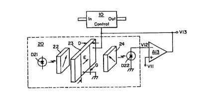
In another embodiment, a simple inexpensive reference attenuator is used to
control the main attenuator. This has a nearly identical electro-optic plate
as in the
main attenuator, but in a much simpler and less expensive attenuator
configuration
as illustrated in Fig. 18. The main attenuator is illustrated by the block 10
having an
optical input port, an optical output port, and an electrical control port.
The
reference attenuator, block 20, contains electro-optic components comprising a
light
source D21 such as a light emitting diode or laser, a linear polarizes 22, an
electro-
optic phase retarder 23, a second linear polarizes 24, and a photodiode light
detector
D22. The electro-optic phase retarder has two electrodes separated by a gap,
G, and
an optical path length, D.
Physically, the polarizers are cemented to either side of the electro-optic
plate and the two diodes face each other from either side. Alignment is
usually not
critical because the beams are fairly large and the optical path is simple.
This
system is stable with temperature, however.
Referring again to Fig. 18, the reference attenuator 20 and the main
attenuator 10 have the same voltage applied. They are also in close physical
proximity so that they experience similar environmental changes. The first
polarizes
is at an approximately 45° angle to the illustrated electric field
direction caused by a
voltage V 13 on the electro-optic plate 23. If the second polarizes is at
90° to the
first, the configuration is normally-off, i.e., with no voltage on the electro-
optic plate
CA 02328089 2000-10-10
WO 99/67679 PCT/US99/07761
-29-
(assuming na natural birefringence) no light reaches the detector. The
electric field
in the electro-optic plate 23 is transverse to the direction of beam
propagation and
the electrodes are separated by a gap, G. When a voltage is applied to the
electro-
optic plate, the field-induced birefringence rotates the optical polarization
direction
so that some of it can pass through the crossed polarizes and reach the
detector.
The mechanism is that light source D21 is linearly polarized by the polarizes
22. The polarized light has equal components perpendicular and parallel to the
electric field at 45°. With a voltage applied, those that are parallel
are retarded in
optical phase as they travel through the plate's thickness D. The effects may
be
visualized as rotating the polarization direction of the beam. When a half
wave
voltage is applied, the component parallel to the beam is 180° out of
phase with the
perpendicular component so that its direction is reversed. The net result is
that the
overall beam is polarized at 90° to its original direction and passes
through the
second polarizes. The 45° angle is not critical, but deviations require
a higher V13
1 S to produce the same modulation. A normally-on version can be obtained by
aligning both polarizers. Both versions have the same theoretical T(V) formula
as
given above for the more complicated attenuator.
It is not necessary for the reference and the attenuator 30 to function
identically, as long as they have the same environmental dependence. The major
requirement is that the main and reference electro-optic plates must have the
same
polarization (P), and the same applied electric field. This can be obtained by
using
the same gap between electrodes and electrically connecting the electro-optic
plates.
A problem may arise, however, if they have the same optical plate thickness,
D. As
illustrated in Fig. 1, the modulation becomes double valued for V > V,~.
Therefore,
D for the reference should be adjusted so that V~ on the main attenuator can
be
reached before the reference. Otherwise, positive feedback will result in the
reference.
From Equations 1 and 2, for a purely quadratic electro-optic effect,
(3) Vn = (~,GZIn3RDm )~' and (4) Dd = ~,GZ /n3R{Vn + OV)2
can be used to calculate Vn for the main attenuator and the path length, Dd
for the
reference. OV provides a margin of safety. It should be as small as possible
to keep
the two pieces closely matched. R is used instead of g because its value is
more
CA 02328089 2000-10-10
WO 99/67679 PCTNS99/07761
-30-
readily available and is an approximation to the mean of the hysteresis
values. For
materials for which n and R are not known, equations (3) and (4) can be used
to
scale the results of a Vn at different wavelengths. In particular, for PLZT
ceramics,
there is a batch to batch variation in R and scaling may be essential for
precise
results.
Other differences between the main and reference are less critical. For
example, the first polarizer 22 in the reference blocks half the light from
the source
D21. This is not a problem because one can find light sources D21 and
detectors
D22 which yield a high enough signal-to-noise ratio. As a second example, in
this
simple configuration, light makes only one pass through the electro-optic
plate 22,
whereas the attenuator can be used in a reflection mode in which the light
makes two
passes through the electro-optic plate in the attenuator 30. In this case, Dm
is about
double the physical thickness.
If the gain of amplifier A13 is large enough, then a voltage V 11 applied to
its positive input will cause the output voltage V 13 to increase until the
signal V 12
from the photo detector D22 and transimpedance amplifier equals V 11. A change
in
environmental parameters will initially change V 12 but the amplifier changes
V 13 to
compensate. If the reference 20 and controlled attenuator 30 are in the same
environment, then the compensation will be suitable for both. Since the photo
detector voltage V 12 is independent of hysteresis, V 13 will automatically be
adjusted to compensate for that, also. In other words, by measuring an effect
that
depends on the polarization there is no need to measure the charge and
polarization
as in the first embodiment.
The principles of operation may be further understood by considering a
working prototype example. The circuitry for this embodiment is illustrated by
the
schematic, Fig. 19. The stability of the device depends on the stability of
the
reference light source. The reference attenuator 20 was modified to include a
partially reflecting minor 21 that reflects a small portion of the light from
the source
D21 to a second photodiode light detector D23. In conjunction with amplifier
Al l,
this forms a feedback loop so that the output from D21 stays constant at a
value
determined by the potentiometer P 11. Feeding D21 with a current source is
possible, but it was found that the light output was too sensitive to
temperature
CA 02328089 2000-10-10
WO 99/67679 PCT/US99/07761
-31
changes even with an attempted temperature compensation of the current source.
With the illustrated approach, the main requirement is that the light sensors
D22 and
D23 are insensitive to temperature changes. (Phototransisitors can be
temperature
sensitive; photodiodes are preferred.)
The electro-optic plate 23 was made from 400 ~m thick 9/65/35 PLZT hot-
pressed bulk ceramic as was the electro-optic plate in the main attenuator.
For both
the reference and main attenuator, the received plates were cut and polished
to
achieve desired dimensions. The light source D21 is an 0.88 ~m GaAs light
emitting diode. The photo detector D22 and D23 are silicon photodiodes. Use of
1.33 wm emitting and detecting photodiodes yielded similar results, but are
more
expensive. Amplifier A12 acts as a transimpedance amplifier and converts the
photocurrent from D22 into a voltage V 12. (In practice, a transimpedance
amplifier
is necessary for D23, also.) Capacitor C13 in conjunction with resistor R13
rolls off
the gain so that the overall feedback loop is stable.
The attenuator was controlled by an external voltage V 14 fed to one end of a
potentiometer P 13. The other end was connected to a much smaller value
potentiometer P14 that can be used to adjust for various small offsets in the
loop.
The voltage V11 at the wiper of P13 was connected to the non-inverting input
of
high voltage amplifier A13 with a supply voltage V 15. This is being operated
as an
integrator so that the voltage V 13 continues to change as long as there is a
difference
between V 11 and V 12.
Component values used in the prototype were: R12 = 200 kS2, R33 = 100 kS2
and C13 = 22 pf. C13 must be made large enough, or some other compensation
scheme used, to keep the feedback loop stable. V 15 must be greater than the
full
modulation voltage required by the attenuator 30 (150 volts or more). The
model
PA42a high voltage amplifier was also used in this circuit.
For a normally-off attenuator, to maximize the transmission at zero input,
V 14 is set to zero and P 14 is adjusted between positive and negative
voltages V 1 S
and V16 until the attenuation in the attenuator is zero, i.e., the
transmission is
maximized. A value of V 14 which it is desired to correspond to zero
transmission
through the attenuator 30, e.g., five volts, is applied and P13 adjusted until
that is
obtained. Then, V 14 is set between zero and five volts to control
attenuation.
CA 02328089 2000-10-10
WO 99/67679 PCTNS99/07761
-32-
Normally-on reference attenuators operating at 0.88 ~m were made to
control both and normally-on and a normally-off main attenuators operating at
1.55
~m light. For two of them, typical dimensions and measured V,~ voltages are
listed
in the following table:
11~. attenuator ~, (um) ~'(.~~1 D l.p V~~-(Vl
on main 1.55 260 600 235
reference 0.88 250 200 270
off main 1.55 400 1,280 272
reference 0.88 385 540 279
It is desirable to make the gap in the main and reference the same subject to
practical
limits. The ideal optical lengths for the reference were calculated after
measuring the
main modulators and scaling using Equations (3) and (4). For reference
purposes
nominal values for PLZT are n = 2.45 and R = 2.53x10''6 m/Vz at 0.88 um and n
=
2.3 and R = 2.4x10''6 m/VZ at 1.55 wm.
Fig. 20 shows the attenuation of the main attenuator as a function of input
voltage, V 14, for the normally-on attenuator. V 13 = 0 volts at the origin
and
increases until attenuation is complete. There is some curvature as the
attenuation
approaches zero and the transmission rises again. This is because the feedback
controls the transmission of the reference, Td, where Td = cosz(V 13/Vnd).
Substituting V 13 into a similar equation for the main attenuator,
theoretically, Tm =
cost[(Vnd)/V,~n)ZCOS 1(Td'~)]. When the half wave voltages are equal, Tm = Td.
Fig. 21 shows the attenuation of a normally-off attenuator with potentiometers
P13 and P14 modified to compare with the normally-on attenuator. Here, V13 = 0
volts when the transmission is zero and increases to the left.
Both figures show a trace from 0 to 100% and back. Hysteresis was smaller
than the noise in the scope trace. Without any compensation, hysteresis is
quite
marked.
The temperature stability was measured by heating and cooling from 25
°C to
75 °C over a period of one hour. The attenuation was set to 1 dB (to
make sure the
circuits were active) and the change in attenuation measured. The variation in
attenuation was 0.15 dB for the normally-off modulator and .05 dB for the
normally-
CA 02328089 2000-10-10
WO 99/67679 PCT/US99/07761
-33-
on modulator. When they were set to 20 dB of attenuation, the nornzally-off
attenuator varied by 0.6 dB and the normally-on one by 1.5 dB. The latter
represents a 30% change, but that is only 0.3% of the input.
It should be noted that, it is quite important that the electro-optic plates
are as
S nearly matched as possible. They can be from the same ceramic plate and be
cut and
polished in the same way. Also, it was noted that the use of larger beam
diameters
in the main modulator produced better results. This can be related to the use
of large
beam diameters in the reference modulator. The use of different wavelengths,
0.88
pm and 1.33 ~tm, did not seem to make a difference. This may not be true for
all
electro-optic materials, however.
In the case of electro-optic phase retarders which use linear effects, similar
principles apply with modifications of Equations 3 and 4. If however, as in
liquid
crystal-based phase retarders, the fields are parallel to the light beam, then
the gap
between electrodes, G, and the optical length, D, are the same. Then, the
optical
length of the reference attenuator can not be changed without changing the
electric
field. However, the voltage applied to the reference attenuator can be made
slightly
less than that applied to the main attenuator in order not to reach the double
valued
region of the reference.
PZT, instead of PLZT, is used for its piezoelectric effect in which the field
induced strain has a quadratic dependence. It also has a quadratic electro-
optic
effect, but is not used in optical applications because of poor optical
transmission.
However, it is not opaque. Thus, if a PZT mechanical actuator replaces the
main
attenuator and a PZT electro-optic plate replaces the plate in the reference
attenuator,
the voltage on the actuator can be controlled in the same way. If actuator
movement
is calibrated against the input voltage that controls the optical
transmission, then the
mechanical drift with temperature can be compensated. This application is not
limited to PZT, but only to materials which have both a piezoelectric effect
and a
practical electro-optic effect.
Another embodiment of the invention that is not limited to a particular type
of
attenuator is illustrated in Fig. 22. A light beam 31 impinges on an optical
splitter
41 that passes most of the light as the beam 32, but diverts a fixed fraction,
F31, as
light beam 33. The light from the beam 32 passes through a voltage
controllable
CA 02328089 2000-10-10
WO 99/67679 PCT/US99/07761
-34-
attenuator 50 that attenuates the light that emerges as beam 34 that, in turn,
impinges
on a second optical sputter 42. Similarly to the first splitter 41, most of
the light
passes to an output beam 35, but a fraction, F32, is diverted as beam 36.
The splitters 41 and 42 can be made from a dichroic mirror or, alternatively,
partially reflecting metal films on transparent substrates. If the light beams
are
carried by fiber optic cables, commercially available couplers can be used. If
the
light beams are carned by surface wave guides, tapping off a small fraction to
divert
the fraction into an adjacent waveguide can be used and the output coupled out
via
fiber-optic cables.
Light from the first optical splitter 41 is made to impinge on a light sensor
such as a photodiode D31. This generates a photocurrent, I1, proportional to
the
light amplitude that is converted into a voltage by the transimpedance
amplifier
A31. The voltage is simply V 1 = I1 ~R3I . In terms on input power, P;, this
is V34 =
k31 ~F31 ~Pi~R31 where k31 is the conversion factor (amps/watt) for the
photodiode
D31. Similarly, photodiode D32 converts the light from cable 36 into a current
that,
due to amplifier A32 and resistor R32 produces a voltage, V32, given by V32 =
k32~F32~Po~R32 where Po is the output power.
A potentiometer P33 provides an attenuated value of V34, namely, V31 =
aV34, where a is the attenuation of P33. V31 is connected to the non-inverting
input of amplifier A33, V32 is connected to the inverting input and the
output, V33,
is connected to the control port of the optical attenuator 51. Assuming A33
has
sufficient gain, it will produce a control voltage, V33, sufficient to make
V32 = V31.
As illustrated, the optical attenuator S 1 is normally non-attenuating and
increasingly
negative control voltages increase the attenuation. The overall attenuation,
Po/P;, is
given by a(k31 ~F31 ~R31)/(k32~F32~R32). If R31 or R32 is adjusted so that
k31 ~F31 ~R31 = k32~F32~R32, then Po = aP;. P33 may be omitted and R31 used
alone to control the attenuation. However, this may result in an attempted
setting
requiring Pa to be greater than P; which is not possible. As in the previous
embodiment, C33 is increased until the feedback loop is stable. P33 may be
replaced by an analog multiplier to obtain a voltage controlled input.
In this embodiment, the precision of the control also depends on matching the
light sensors D31 and D32 with respect to temperature variations.
CA 02328089 2000-10-10
WO 99/67679 PCT/US99/07761
-35-
In another embodiment, an absolute transmission controller may be obtained
by leaving out the first beam splitter, 41, diode D31, and amplifier A31 and
associated circuitry and using V31 to control the absolute intensity. In this
case,
D32 and associated circuitry must be stable on an absolute basis.
Refernng to Figs. 23A and B, further details of a variable attenuator with a
compensator system in accordance with the present invention are provided. This
embodiment illustrates the principles of operation of a variable attenuator
(VOA) 50
in parallel with a reference attenuator (VOA')120. The circuitry for this
embodiment
is illustrated by the schematics, Fig. 23A and B. The stability of the device
depends
on the stability of the reference light source. The reference attenuator 120
was
modified to include a partially reflecting mirror 20 that reflects a small
portion of the
light from the source D21 to a second photodiode light detector D23. A light
emitting diode driver represented by block 100 is a part of a feedback loop to
keep
the output from D21 a constant.
The light source D21 is an 0.88 pm GaAs light emitting diode. The photo
detector D22 and D23 are silicon photodiodes. An offset voltage compensator
block
130 is used to adjust for various small voltage offsets in the compensator
circuit. A
high voltage driver circuit block 150 is coupled to the compensator 120 and to
the
VOA 50 such that the same high voltage and same electric field distribution is
present in both VOA and compensator. An environmental change to both
compensator and VOA will then cause the same polarization change and produce a
change in optical transmission through the compensator. Feedback from the
electrical circuit will then force the optical transmission through the
compensator
and through the VOA to return to its intended value, as described earlier.
Referring to Fig. 24, another embodiment of a variable attenuator with a
compensator system in accordance with the present invention is provided. The
reference attenuator 210 was modified to include a partially reflecting mirror
20 that
reflects a small portion of light from the light source D21 to a feedback Ioop
which
includes the light emitting diode driver circuit block 200. The feedback Ioop
keeps
the output from D21 constant.
The light source D21 is an 0.88 pm GaAs light emitting diode. A
transimpedance amplifier 220 converts the photocurrent from the detector 230
into a
CA 02328089 2000-10-10
WO 99/67679 PCTNS99/07761
-3 6-
voltage. A high voltage driver 240 is coupled to the transimpedance amplifier
220.
Referring to Figs. 25A and 25B, another embodiment of a variable attenuator
is shown in which the output power of the device is tapped and a feedback
circuit
maintains the output level constant. In this mode of power control, the
attenuation
may vary but the output power level is kept constant. This embodiment, having
the
output tap, is useful as a power limiter.
The embodiment comprises a transimpedance amplifier 300 which is coupled
to a high voltage driver 310. The transimpedance amplifier 300 converts the
photocurrent from the detector 320 (LED) into a voltage. The variable
attenuator 50
is coupled to the high voltage driver 310. The light beam from the attenuator
impinges on an optical sputter 20 which diverts a fixed fraction of light to
the
detector 320 to form a feedback loop while most of the light passes to an
output
beam.
Refernng to Fig. 26, a wavelength division multiplexing (WDM) fiber-optic
telecommunications system using a preferred embodiment of the present
invention is
shown. The variable attenuator of the present invention attenuates the power
into
the fiber amplifier. A fiber-optic telecommunications system 600 includes
input
wavelength division multiplexers (WDM) 602, a laser module 605, fiber coupler
610, a filter 620, the variable attenuator 630 of the present invention, a
fiber
amplifier 640 coupled to a fiber coupler 650, a laser module 655, a filter
660, and an
output WDM. The output of the laser module 605 is coupled with the input WDM
in the fiber coupler 610. After filtering the optical signal is attenuated in
the
variable attenuator 630 before forming an input into the fiber amplifier. Once
amplified, the signals are coupled with the output of the laser module 655 and
filtered by filter 660. The signals provide a wavelength division multiplexed
optical
signal carried to remote subscriber locations.
Referring to Fig. 27, the variable attenuator of the present invention is
illustrated in DWDM systems. The variable attenuator balances power in the
channels having different wavelengths. A dense WDM, system which operates on
densely spaced wavelengths includes an input fiber 702 carrying optical
signals of
different wavelengths which form the input into a demultiplexer 710 which
CA 02328089 2000-10-10
WO 99/67679 PCT/US99/07761
-37-
demultiplexes the combined input optical signal. The demultiplexed optical
signals
and added channels ~,1 - ~,,,, then form the input to separate switches 720.
The output
of the switches then form the input to the attenuators 740 of the present
invention.
The attenuators are used for power balancing in the DWDM system. By this
approach of modulating separate wavelengths, a subscriber location can be
provided
with multiple services from a single laser source from a single fiber. The
output
signals from the attenuators 740 are then multiplexed in multiplexes 760 and
outputted on an optical fiber 770. If required the output of the attenuators
can be
tapped using the monitoring taps 790.
While the invention has been described in terms of attenuators and actuators,
other types of devices can be produced. For example, a power leveler that
controls
the log of the intensity could be made by converting the output of the light
sensors,
D22, in Embodiments #2 and #3, into a logarithmic representation. As another
example, the main attenuator could be replaced by a simple phase retarder
controlled
by the reference modulator. The amount of phase shift in the retarder could be
calibrated against transmission in the reference modulator and thereafter
controlled.
In this application, since transmission versus phase is non-linear, use of
analog-to-
digital and digital-to-analog converters in conjunction with a digital
processor would
be useful. The latter approach would also be useful in the piezoelectric
actuator
embodiment.
Besides PLZT and PZT, without being an exhaustive list the following
materials may be used: Pb(Zr,Ti)03 , Pb(Mg,Nb)03, and a solid solution of
Pb(Mg,Nb)03 and PbTa03. Further, the embodiment of the present invention can
be
used in an optical fiber communication system, in particular for dense
wavelength
division multiplexing (DWDM). The embodiments of the present invention can
attenuate the power input to optical fiber amplifiers. In addition, in another
DWDM
application, the embodiments of the present invention can balance power in
different
wavelength channels.
While the preferred embodiments have been sufficiently described to enable
one skilled in the art to make and use them, it should be appreciated that
other
obvious alternatives, modifications, or equivalents will be apparent to those
in the
field of electro-optics. In particular, even without applying a voltage, a
strong
CA 02328089 2000-10-10
WO 99/b7679 PCT/US99/07761
-3 8-
external electric field will affect the phase retarder and thus the device can
be used
as an electric field sensor.