Note: Descriptions are shown in the official language in which they were submitted.
CA 02328327 2000-12-14
Plug Connector
The invention relates to a plug connector for mounting on a
circuit board and having a carrier body in which at least one
surface mounting contact member is disposed which comprises,
at one end, a plug-in region for connection with a
complementary plug connector and, at the other end, a
connecting region which may be connected with the conductor
track of a circuit board.
The surface mounting technology offers some advantages over
conventional plug connectors which are provided with pass-
through mounting contact members, both during the mounting
process and as regards the transmission speed for signals from
the surface mounting contact member to the conductor track of
the circuit board. In order to accomplish a reliably soldered
connection, particular attention must be paid to the
coplanarity of the terminal ends during the manufacturing
process for the plug connectors. It has turned out that the
height deviation of the connecting region must not exceed 0.1
mm if all connections shall be safely soldered. However, such
slight tolerances may only be ensured either via a very
expensive manufacturing process leading to a product which
reliably keeps to the corresponding tolerances, or via a
sorting process following the manufacturing process, in which
all those plug connectors are sorted out which do not keep to
the required tolerances. However, this leads to a high reject
rate and, accordingly, to high overall production costs.
Another problem with regard to surface mounted contact members
consists in that the soldered joint between the contact member
and the circuit board is less rigid than a soldered joint with
CA 02328327 2004-10-07
23292-128
2
through-type contact members, more particularly under shear
stress. On the one hand, this fact is critical in view of
the forces acting on the plug connector during insertion
into a complementary plug connector and, on the other hand,
in view of mechanical stresses arising from differences in
the thermal expansion of the circuit board and the plug
connector or due to flexure of the circuit board.
Therefore it is the object underlying embodiments
of the invention to further develop a plug connector of the
type initially mentioned to the effect that despite low
manufacturing expenditure a reliable connection is
guaranteed between the connecting region of the surface
mounting contact member and the conductor track of the
circuit board and that significant mechanical forces are
prevented from acting on the soldered connection after
soldering.
In order to meet this object, it is provided for
in accordance with the invention that the contact member
comprises a connecting member which is connected with the
connecting region in a mechanically flexible and
electrically conductive manner and may be soldered to the
conductor track of the circuit board. The basic idea
underlying the plug connector according to the invention
resides in configuring the surface mounting contact member
in multiple parts and in taking advantage of a predetermined
slidability between the different parts, i.e. the actual
contact member and the connecting member in particular, for
tolerance compensation during assembly of the plug connector
on the one hand and for permanent movability during
operation of the plug connector on the other hand. The
tolerance compensation, which is now realized automatically,
reduces manufacturing process requirements so that there
result lower costs. Mechanical decoupling between the
CA 02328327 2004-10-07
23292-128
3
circuit board and the surface mounting contact member
increases the durability of the soldering points since there
occurs a relative displacement between the connecting member
and the contact member, but no mechanical strain on the
soldering points when certain mechanical stresses between
the circuit board and the contact member are exceeded.
According to one aspect of the invention, there is
provided a plug connector for mounting on a circuit board
and having a carrier body in which at least one surface
mounting contact member is disposed which comprises, at one
end, a plug-in region for connection with a complementary
plug connector and, at the other end, a connecting region
which may be connected with the conductor track of a circuit
board, characterized in that the contact member comprises a
connecting member which is connected with the connecting
region in a mechanically flexible and electrically
conductive manner and may be soldered to the conductor track
of the circuit board wherein the connecting member is
slidably mounted on the connecting region and before the
plug connector is mounted on the circuit board, the
connecting member is in a mounting position in which it
projects farther from the plug connector than after
mounting.
Thus, the connecting member may be attached to the
surface mounting contact member before the plug connector is
mounted on the circuit board already and need not be handled
as a separate component during the assembly process.
In this manner, the desired tolerance compensation
results automatically when the plug connector is put onto
the circuit board since the projecting connecting members
are shifted into the correct position during putting-on.
CA 02328327 2004-10-07
23292-128
3a
According to the preferred embodiment, it is
further provided that the connecting member is a resilient
clamp engaging the connecting region. On the one hand, this
spring effect may ensure that the desired contact force
between the clamp and the connecting region of the surface
mounting contact member exists even after a long operating
time. On the other hand, one may adjust via the spring
force amount which mechanical stress must act between the
surface mounting contact member and the connecting member
before there will occur a relative displacement.
According to a preferred variant, it is provided
that the connecting member is formed to be spherical. This
makes it possible to contact the connecting region from
almost any direction since there always result two
diametrically opposite contact points on the connecting
region, irrespective of slight relative displacements.
The contact member is preferably provided with an
insulating body which constitutes a guide for the clamp.
The guide
CA 02328327 2000-12-14
' 4
ensures that the clamp is in the desired position before
assembly of the plug connector so that it is automatically
shifted from the mounting position into the correct position
for soldering. The guide is more particularly required in
conjunction with the spherical connecting region since the
latter cannot provide any guide for the clamp.
The insulating body is preferably provided with contact faces
for the clamp, which are opposite each other at a spacing
larger than the corresponding dimension of the clamp in this
region. This dimensioning of the parts relative to each other
not only enables a translatory shifting of the clamp on the
guide, but also a pivot and tilt movement which may be
necessary for the compensation of mechanical stresses which
may result from bending of the circuit board or from
differences in the thermal expansion between the plug
connector and the circuit board.
According to an alternative variant, it is provided that the
2U connecting region has a rectangular cross-section. In this
case, a guide for the connecting member is realized due to the
shape of the connecting region already. The alternative
variant preferably provides that the clamp is provided with
several guide surfaces which may engage opposite edges of the
connecting regions. This makes sure that the clamp does not
laterally slip off the connecting region. The guide surfaces
may be formed on bent-off noses of the clamp.
According to the preferred embodiment, it is provided that the
resilient clamp comprises two legs engaging the connecting
region, and a bottom connecting the two legs with each other
and facing towards the circuit board, and that the bottom is
provided with a spacer which ensures a predetermined spacing
between the bottom and the circuit board. The spacer prevents
the bottom of the clamp from bearing against the circuit board
during assembly of the plug connector and from fully forcing
the solder paste, which had previously been applied to the
circuit board, away in this region, which would result in an
inadequate solder joint.
CA 02328327 2000-12-14
It is preferably provided that the spacer is formed as a
raised portion which may bear with its apex against the
circuit board. The apex of the raised portion forms a tip
5 which reliably penetrates the solder paste. This makes sure
that the spacer actually bears against the circuit board
rather than against a solder paste pad so that the correct
spacing between the bottom of the clamp and the circuit board
is ensured.
According to an alternative embodiment, it may be provided
that the connecting member is connected with the connecting
region via a bond wire. Thus, a further additional component
is used in this case in order to create the electrically
conductive connection between the connecting member and the
connecting region of the contact member. The bond wire enables
relative movability of the parts.
According to the preferred embodiment of the invention, there
is further provided at least one pass-through mounting contact
member. In this manner, two advantages result therefrom: on
the one hand, the pass-through mounting contact member enables
a sort of preliminary fixing of the plug connector after it
has been put onto the circuit board and before soldering. On
the other hand, the pass-through mounting contact member
ensures, due to its higher holding force in the circuit board,
good mechanical fixing of the plug connector so that there is
less strain on the soldered joints of the surface mounting
contact members from forces acting on the plug connector.
Preferably, the pass-through mounting contact member is an
earth contact and the surface mounting contact member is a
signal contact. This configuration takes into account the
advantages offered by a surface mounting contact member in
view of signal velocity; maximum signal velocity is of
secondary importance for an earth contact.
According to one embodiment of the invention, the plug
connector is a card-edge plug connector. Plug connectors of
CA 02328327 2000-12-14
6
that kind are used for a multipole and pluggable connection
between a circuit board and a cable and, respectively, another
circuit board for the transmission of electrical signals. The
contact members are disposed in an insulating body in rows and
columns. Via a suitable combination of surface mounting
contact members and pass-through mounting contact members
there may be obtained a card-edge plug connector which is both
anchored on the circuit board with high mechanical strength,
namely by means of the pass-through mounting contact members,
and offers a high signal transmission velocity, namely due to
the surface mounting contact members. No longer does the
problem occur, which had hitherto arisen in the prior art,
namely that the surface mounting contact members of a card-
edge plug connector are shear-strained due to the location of
the plug connector since, on the one hand, the pass-through
mounting contact members introduce a large part of the
occurring forces directly into the circuit board and, on the
other hand, a possible relative displacement between the plug
connector and the circuit board does not result in any stress
on the soldered joints between the surface mounting contact
members and the conductor tracks since the mufti-part
configuration of the contact member enables a relative
displacement with the connecting member.
According to a further embodiment, it is provided that the
plug connector is a coaxial-contact plug connector. This
configuration also takes advantage of the combination of a
surface mounting contact member and a pass-through mounting
contact member, more particularly when the surface mounting
contact member constitutes an inner conductor of a coaxial
contact member and the pass-through mounting contact member is
an earth sheet metal connected with an outer conductor of the
coaxial contact. Reference is made to the above explanations
in respect of the advantages of this combination of a signal
contact and an earth contact.
Advantageous configurations of the invention may be taken from
the subclaims.
CA 02328327 2000-12-14
7
In the following, the invention will be described upon
reference to two preferred embodiments which are represented
in the enclosed drawings. Therein:
- Fig. 1 is an isometric sectional view of a plug connector
according to a first embodiment of the invention;
- Fig. 2 is an isometric representation of the individual
components of the plug connector of Fig. l;
- Fig. 3 is an enlarged view of the surface mounting contact
members used in the plug connector of Fig. 1;
- Fig. 4 is a side view of the plug connector of Fig. 1 with
two connecting members in two different positions;
- Fig. 5 is an isometric representation of the contact members
according to a variant of the plug connector shown in Fig. 1,
some components not being shown for better clarity;
- Fig. 6 is a sectional side view of a plug connector
according to a second embodiment of the invention;
- Fig. 7 is a sectional view of a plug connector according to
a variant of the embodiment shown in Fig. 6;
- Fig. 8 is a sectional view of a plug connector according to
a second variant of the embodiment shown in Fig. 6;
- Fig. 9 is an isometric view of a connecting member for use
with the plug connector according to the second embodiment;
and
- Figs. l0a and lOb are each sectional views of a plug
connector according to the second embodiment in a condition
before and after mounting on a circuit board.
CA 02328327 2000-12-14
8
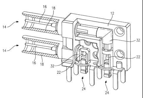
Figs. 1 and 4 show a plug connector according to a first
embodiment of the invention. This concerns an angled coaxial
plug connector provided for mounting on a circuit board.
The plug connector comprises a carrier body formed of two
housing portions 10, 12 which consist of metal and in which
coaxial plug contacts 14 are accommodated. Metallized plastic
may alternatively used as the material for the housing
portions 10, 12 too. In any event, the housing must be
electrically conductive to ensure shielding.
The two coaxial plug contacts 14 each consist, in a known
manner, of a pin-shaped inner conductor 16 and a sleeve-shaped
outer conductor 18. The sleeve-shaped outer conductor is
electrically conductive and is in electrically conductive
connection with the housing constituted by the two housing
portions 10, 12.
The inner conductor 16 is part of a surface mounting contact
member 20 which extends up to the connecting side of the plug
connector, i.e. towards that side with which the plug
connector is mounted on the circuit board.
The surface mounting contact member 20 (see Fig. 3 in
particular) comprises a connecting region 22 which is
configured to be spherical. The surface mounting contact
member 20 further comprises a connecting member 24 which is
provided for engaging the connecting region 22 in electrically
conductive connection. Here, the connecting member 24 is
formed as a resilient clamp with two legs 26 being connected
to each other by means of a bottom 28. On the bottom, there is
provided, on the side facing away from connecting region 22, a
spacer 30 which is configured as a stamping in such a manner
that a comparatively pointed apex is formed. The function of
the spacer 30 will be explained in the following.
The surface mounting contact member 20 further comprises an
insulating body 32 which serves for insulation against the
electrically conductive housing. Insulating body 32 is
CA 02328327 2000-12-14
9
configured as a guide for connecting member 24 about the
connecting region 22 of the surface mounting contact member
20. The guide consists of a guide web 34 and contact faces 36
for limiting the guide web 34. Locating surfaces 36 are
situated opposite each other at a spacing which is larger than
the width of the legs 26 so that the connecting member 24 may
be slightly tilted in the guide.
Finally, the plug connector is provided, on the connecting
side, with a pass-through mounting contact member 38 which is
formed as an earth sheet metal. This one is in electrically
conductive connection with the housing constituted by the two
housing portions 10, 12 and comprises terminal legs 40
engaging, for instance, corresponding openings of the circuit
board, on which the plug connector is to be mounted, as well
as recesses 42 through which the surface mounting contact
member respectively extends.
For assembly, the surface mounting contact members 20, the
sleeve-shaped outer conductor 18 as well as the earth sheet
metal serving as the pass-through mounting contact member 38
are inserted in suitable receptions of the two housing
portions 10, 12. The connecting member 24 may be slipped onto
the guide web 34 of the insulating body 32 up to a mounting
position in which it is autofixed on the surface mounting
contact member. This position is shown in Fig. 4 in respect of
the right connecting member 24.
In this finished assembled condition, the coaxial plug
connector may be mounted on a circuit board. For this purpose,
the circuit board is first coated with a solder paste at the
locations which are provided for connection with the inner
conductor 16 of the coaxial plug contacts 14. Subsequently,
the coaxial plug connector is put onto the circuit board, the
terminal legs 40 of the pass-through mounting contact member
38 penetrating into suitable openings of the circuit board.
During the process of putting the plug connector onto the
circuit board, the connecting member 24 immerses into the
previously applied solder paste, the spacer 30 reliably
CA 02328327 2000-12-14
forcing away and penetrating the solder paste with its apex so
that it rests on the circuit board. This ensures that the
bottom 28 comprises, in all the remaining regions, a
predetermined spacing from the circuit board, which is given
5 by the height of the spacer, preferably is 0.1 mm and is
completely filled with solder paste.
The mounting position of the contact members 24 is selected
such that the spacer 30 bears against the circuit board before
10 the terminal legs 40 are completely pushed into the circuit
board. Thus, there results a relative displacement between the
connecting member 24 and the connecting region 22
approximately at the end of the process of putting the plug
connector onto the circuit board, whereby the legs 26 of the
connecting member formed as a clamp are pushed onto the
connecting region 22. This condition, in which the electrical
connection between the connecting member 24 and the inner
conductor 16 is ensured independently of the respectively
existing tolerances, is shown for the left connecting member
24 in Fig. 4.
As soon as the plug connector is correctly put onto the
circuit board, the surface mounting contact members may be
soldered, a reliable soldering being ensured due to the
precisely kept spacing between the bottom of the connecting
member 24 and the circuit board. This spacing between the
bottom 28 of the connecting member 24 and the circuit board is
not influenced by tolerances of the plug connector or by an
uneven circuit board surface since possible tolerances are
compensated in that the contacting member is pushed onto the
connecting region 22 of the surface mounting contact member in
differing lengths.
Fig. 5 shows the surface mounting contact members as well as
the pass-through mounting contact members for a coaxial plug
connector which slightly alters the embodiment of Fig. 1 and
is no longer formed to be angled, but comprises rectilinearly
extending contact members. The surface mounting contact
members of the variant shown in Fig. 5 substantially
CA 02328327 2000-12-14
11
corresponds to the shorter surface mounting contact member of
the embodiment shown in Figs. 1 to 4. The difference merely
consists in that the connecting member 24 does no longer
engage the connecting region 22 transversely with respect to
the longitudinal direction of the contact member, but is
pushed onto the connecting region parallel with respect to the
longitudinal direction of the contact member. The contact as
such, which results between the legs of the connecting member
24 and the connecting region 22, remains unchanged since two
diametrically opposed contact spots result independently of
the direction in which the connecting member is pushed onto
the connecting region.
Fig. 6 shows a plug connector according to a second embodiment
of the invention. This concerns a card-edge plug connector
serving for the connection of circuit boards. It usually
comprises a plurality of contacts which are disposed in
several adjacent columns. Just a single column may be seen in
the sectional representation of Fig. 6.
The embodiment shown concerns an angled multiple-contact strip
since the individual contacts are each angled by 90° and
formed as contact springs on the connecting side of the plug
connector. Consistent therewith, the complementary plug
connector which is inserted into the shown plug connector is a
blade-contact strip. Of course the embodiment shown may also
be formed as a blade-contact strip.
In this embodiment, the housing portion 10 constitutes an
insulating carrier body which may optionally be provided with
a shielding. The individual contacts are held in the carrier
body, they consisting of two pass-through mounting contact
members 38 which on their connecting side engage openings 50
of a circuit board 52 as well as of a surface mounting contact
member 30 being provided with a connecting member 24 on its
connecting side. The precise configuration of the connecting
member 24 as well as the cooperation with the surface mounting
contact member 20 will be explained in the following.
CA 02328327 2000-12-14
12
Fig. 7 represents a variant of the embodiment shown in Fig. 6.
In contrast to the embodiment of Fig. 7, a contact member 53
is provided instead of the outer pass-through mounting contact
member 38, which member 53 has a bend at its connecting end
which rests on the circuit board and may be connected there
with a corresponding conductor track in surface mounting
technology.
Fig. 8 represents a second variant of the embodiment shown in
Fig. 6. In contrast to the embodiment shown in Fig. 6, this
does not concern an angled multiple-contact strip, but a
straight multiple-contact strip; thus, the contact springs of
the individual contact members extend perpendicularly with
respect to the circuit board plane. A further difference
resides in that no pass-through mounting contact members, but
surface mounting contact members 20 are used exclusively.
Fig. 9 shows the connecting member 24 which is used with the
surface mounting contact members 20 of the plug connectors
shown in Figs. 6 to 8. As regards its structure, the
connecting member substantially corresponds to the connecting
member known from Figs. 1 to 4, however it is slightly
modified.
In the plug connectors shown in Figs. 6 to 8, the connecting
region of the surface mounting contact members 20 comprises a
rectangular cross-section. Thus, the connecting member 24
which engages the connecting region with the two oppositely
situated legs 26, is roughly guided per se. In order to
prevent the connecting member from slipping off the connecting
region, bent-off noses 54 are provided on one of the legs 26
of the connecting member 24, whose surfaces being opposite to
each other act as guide surfaces 56. These may engage the
narrow outer surfaces of the connecting regions 22 and prevent
the connecting member 24 from being tilted excessively or even
from slipping off.
In the following, the mounting process of a plug connector
like the one shown in Figs. 6 to 8 will be described upon
CA 02328327 2000-12-14
13
reference to Fig. 10. After assembly of the .plug connector,
the connecting member 24 is in the mounting position to be
taken from Fig. 10a. In the mounting position, the connecting
member 24 extends comparatively far from the plug connector.
When the plug connector is put onto the circuit board (see
Fig. lOb), the connecting member 24 on the connecting region
22 is further displaced towards the center of the plug
connector. This relative displacement has an end as soon as
the plug connector is completely put onto the circuit board 52
and the optionally provided pass-through mounting contact
members are inserted into the corresponding openings 50. In
this condition, the connecting member 24 may be soldered to
the corresponding conductor track of the circuit board 52
since the required spacing between the bottom of the
connecting member and the circuit board has materialized due
to the spacer 30 being provided.
CA 02328327 2000-12-14
~3a
List of Reference Numerals:
10: Housing portion
12: Housing portion
14: Coaxial plug contact
16: Inner conductor
18: Outer conductor
20: Surface mounting contact member
22: Connecting region
24: Connecting member
26: Leg
28: Bottom
30: Spacer
32: Insulating body
34: Guide web
36: Contact face
38: Pass-through mounting contact member
40: Terminal
42: Recess
50: Opening
52: Circuit board
53: Contact member
54: Nose
56: Guide surface