Note: Descriptions are shown in the official language in which they were submitted.
CA 02328460 2000-12-13
1
ELECTRICAL POWER INTERFACE CONNECTOR
BACKGROUND OF THE INVENTION
1. Field of the Invention
The present invention relates to electrical connectors
and, more particularly, to an electrical power interface
connector crimped to an electrical conductor.
2. Brief Description of Earlier Developments
The commercial demand for ever smaller and more powerful
electronic devices has fueled the miniaturization of
electronic components, such as electrical connectors,
to used in or with the electronic devices . U. S . Patent No .
3,980,380 discloses one example of a conventional
connector comprising a molded dielectric insert having a
plurality of contacts around the periphery of the insert,
and a plurality of blind-end conductor retainer apertures
into which 'insulated conductors are inserted. The blind-
end apertures intersect insulation piercing self-
connection terminal elements of the contacts. The
terminal elements are activated into contact with the
wires by rotating the insert to cam the terminal elements
into the wires. Another example of a conventional
connector is disclosed in U.S. Patent No. 4,749,357,
wherein a power distribution connector has an insulating
block with a bus element supported therefrom, and a
crown-shaped contact located in the block which is
electrically connected to the bus element. Still another
example of a conventional connector is U.S. Patent No.
5,807,145 which discloses a break-contact block having
two identical half-housings with compartments to
accommodate bridge-like contacts and respective springs.
A' further example of a conventional connector is U.S.
Patent No. 5,358,417 which discloses an electrical
CA 02328460 2000-12-13
2
connector comprising an elongated plastic housing with
holes adapted to receive electrical conductors therein.
The plastic housing is heat-staked to retain the
conductors therein. Miniaturization of conventional
electrical connectors has caused conventional connectors
to be very complex in order to ensure an adequate power
interface to wire. This is evident in the afore-
mentioned examples. The complexity of conventional
connectors coupled with their small size has caused the
l0 manufacture of the connectors to be labor intensive, and
hence, costly. Furthermore, additional reductions in the
size of conventional connectors are limited because the
effectiveness of the interface between the conductor wire
and connector is reduced as the size of the connector
decreases. In addition, conventional convectors have
contacts which are provided with a tail section having
interfacing features, such as bendable tabs, to allow the
conductor to be crimped or otherwise attached directly to
the contact. These features are time consuming to
produce especially for contacts interfacing with small
conductors. In addition, due to their small size, these
conductor crimping features of contacts in conventional
connectors are susceptible to damage during connection of
the conductors to the contacts. This may result in an
improper or inefficient interface between conductor and
contacts which may fail during use. The present
invention overcomes the problems of conventional
connectors. For instance, in the present invention,
conductors need not be crimped directly to the connector
contacts to provide an electrical connection
therebetween. This is especially advantageous in
comparison to conventional connectors wherein direct
contact between conductors and contacts is used to effect
a. connection therebetween. ~ The present invention
provides a block section connected to connectors in a
manner which is not prone to failure when connected to
CA 02328460 2000-12-13
A
3
the conductors, and which~is capable of generating much
higher clamping forces on the conductors in comparison to
crimp tabs on conventional contacts and conventional
connectors.
SUMMARY OF THE INVENTION
In accordance with a first method of the present
invention, a method for forming an electrical interface
for an electrical cable is provided. The method
comprises the steps of providing an electrical connector
having a block section, inserting a bare conductor in the
block section, and crimping the block section on the bare
conductor. The block section of the electrical connector
has at least one conductor receiving hole formed in a
first end of the block section. The bare conductor is
inserted into the conductor receiving hole of the block
section. The block section is made from a deformable
conductive material wherein crimping the block section
deforms the conductor receiving hole clamping the
conductor inside the hole.
In accordance with a second method of the present
invention, a method for manufacturing an electrical
connector is provided. The method comprises the steps of
forming a conducting block, forming contact receiving
holes in the conducting block, and forming at least one
conductor receiving hole in the conducting block. The
conducting block is formed from a deformable conductive
material. The conducting block is a one-piece member.
The contact receiding holes are formed in a first end of
the conducting block. The conductor receiving hole is
formed in a second end of the conducting block. The
conductor receiving hole is formed proximate to a side of
CA 02328460 2000-12-13
the conducting block wherein an indentation pressed into
the side of the conducting block deforms the conductor
receiving hole and crimps the conductor located inside
the hole.
In accordance with a first embodiment of the present
invention, an electrical connector is provided. The
electrical connector comprises an interface block. The
interface block has a first end with at least one
conductor receiving hole formed therein. The interface
block has a second end with contact receiving holes
formed therein opposite the conductor receiving hole.
The interface block has a side disposed adjacent to the
conductor receiving hole. The interface block is made
from malleable metal. The side adjacent to the conductor
receiving hole is indented for crimping a conductor
located inside the conductor receiving hole.
In accordance with a second embodiment of the present
invention, an electrical connector is provided. The
electrical connector comprises a block section. The
block section has a bore formed in one end for receiving
a bare conductor therein. The block section has contact
receiving holes in an opposite end of the block section
for receiving contacts. The block section has a side
with an indentation formed by cold pressing a die shape
into the side of the block section. The indentation in
the side of the block section deforms the bore for
crimping the conductor located in the bore to the block
section.
BRIEF DESCRIPTION OF THE DRAWINGS
CA 02328460 2000-12-13
The foregoing aspects and other features of the present
invention are explained in the following description,
taken in connection with the accompanying drawings,
wherein:
5 Fig. 1 is an exploded perspective view of an electrical
power interface connector incorporating features of the
present invention;
Fig. 2 is a perspective view of the power interface
connector in Fig. 1 shown in an assembled configuration
to connected to electrical conductors;
Fig. 3 is an end elevation view of the block section of
the power interface connector in Fig. l;
Fig. 4 is a cross-sectional view of the power interface
connector in Fig. 1 connected to electrical conductors;
and
Figs. 5A-5B are respectively a perspective view and an
end elevation view of an interface block section of an
electrical connector in accordance with a second
preferred embodiment of the present invention.
DETAILED DESCRIPTION OF THE PREFERRED EMBODIMENT
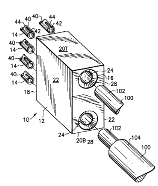
Referring to Fig. 1, there is shown an exploded
perspective view of an electrical power interface
connector 10 incorporating features of the present
invention. Although the present invention will be
described with reference to the embodiments shown in the
drawings, it should be understood that the present
invention can be embodied in many alternate forms of
embodiments. In addition, any suitable size, shape or
type of elements or materials could be used.
CA 02328460 2000-12-13
6
Referring now also to Fig. 2, the electrical connector 10
generally comprises a block section 12 and contacts 14.
The contacts 14 are mounted to the block section 12 to
extend from one end thereof. Electrical cables 100, such
as cables for transmitting power to an electronic
component, are connected to block 12, preferably at an
opposite end. Cables 100 and contacts 14 could, however,
have another arrangement such as a right angle
configuration. The block section 12 forms an electrical
connection between the cables 100 and contacts 14 thereby
providing a power interface to the cables 100. With the
connector 10 mounted to the cables 100, the cables may be
connected to a suitable device, such as, a mating
connector on an electronic component (not shown) for
providing electrical power to the electronic component.
The opposite ends (not shown) of cables 100 may be
terminated in any suitable manner. The electrical
connector 10 may be housed alone or in combination with
other similar electrical connectors in an insulating
housing (shown in phantom in Figure 3) to provide a power
coupling of desired size and electrical capacity.
Referring now also to Figs. 3 and 4, the block section 12
of the electrical connector 10 is preferably a one piece
member made from a soft or malleable metal such as brass
or tellurium copper. In alternate embodiments, the block
section of the connector may be made from any other
suitable deformable conductive material. As seen in
Figs. 1 and 4, the block section 12 is a hexahedron with
a generally rectangular cross-section. The top and
bottom faces 20T, 20B, the side faces 22 and the end
faces 16, 18 of the block section 12 are, substantially
flat. In alternate embodiments, the block section may
have any other suitable shape such as a cylindrical
shape. In still other embodiments, the sides of the
block section may be angled obliquely relative to each
CA 02328460 2000-12-13
7
other or may have surface features formed therein. The
block section 12 has conductor receiving chambers formed
therein. As shown in the figures, the block section
could have two of the conductor receiving chambers 24U,
24L. The upper and lower conductor receiving chambers
24U, 24L are arranged side by side as seen in Fig. 9.
Each chamber 24U, 24L has a closed end 26 and a chambered
opening 28 in one end face 16 of the block section 12.
In alternate embodiments, the block section may have any
suitable number of conductor receiving chambers formed
therein with corresponding openings in one or more sides
or ends of the block section. In other alternate
embodiments, the block section may have several rows of
conductor receiving chambers. The block section 12 also
has contact holding receptacles 30 formed therein. As
seen in Figs. 3 and 4, the block section 12 could have
eight of the contact holding receptacles 30. The contact
holding receptacles 30 are shown disposed in two columns
of four receptacles, though the receptacles may have any
other suitable arrangement. Each contact holding
receptacle 30 has an aperture 32 in the end face 18
opposite the conductor receiving chambers 28 of the block
section 12. Each contact holding receptacle 30
terminates in a blind end 34. The contact holding
receptacles 30, and contact receiving chambers 24U, 24L
in the block section 12 may be separated from each other
(see Fig. 4), although other arrangements (e. g.
superposition) are possible. In alternate embodiments,
the connector block section may have any suitable number
of contact holding receptacles which may communicate with
one or more of the conductor receiving chambers.
The conductor receiving chamber 24U, 24L in the block
section 12 of the connector 10 are sized to generally
CA 02328460 2000-12-13
8
conform to the diameter of the bare conductor 102 of the
electrical cables 100. By way of example, the conductor
receiving chambers 24U, 24L in the block section may have
a diameter of about .075 inches to receive a No. 14 AWG
conductor 102. In alternate embodiments, the conductor
may have any other desirable size and the conductor
receiving chamber in the block section may be sized to
suit. The depth of the conductor receiving chambers 24U,
24L, is sized to provide adequate grip on the bare
l0 conductor 102U, 102L, when the conductor is connected to
the connector 10. For example, in the preferred
embodiment, the conductor receiving chamber 24 for a No.
14 AWG conductor may be about 0.25 inch deep. The
conductor receiving chambers 24U, 24L are located
IS proximate to the faces 20T, 20B, 22 of the block section
12 such that displacement or indention of the faces
deforms the conductor receiving chambers 24U, 24L.
The contacts 14 of the connector 10 may be pin or
receptacle contacts made from a suitable conductive
20 material such as brass, tellurium copper, or phosphor
bronze (only the tail portion 40 of contacts 14 are shown
in Figs . 1-4 ) . The contacts 14 have a mounting, or tail
portion 90 which is held in an interference fit within
the block section 12 to secure the contacts to the block
25 section of the connector. The tail portion 40 of the
connector 14 is resiliently compliant for resiliently
complying with the contact holding receptacles 30 in the
block section 12. For example, the tail portion 40 of
each contact 14 may comprise the generally cylindrical
30 shell 42 (see Fig. 1). The shell 42 has a longitudinal
slot 44. The slot 44 allows the cylindrical shell 42
forming the tail portion 40 of the contact 14 to
resiliently flex inwards when subjected to radial
compression. In alternate embodiments, the shell forming
35 the tail portion of the contacts may have two or more
CA 02328460 2000-12-13
9
longitudinal slots to form a number of cantilevered
spring arms allowing the tail portion to comply with
mating receptacles in the block section of the connector.
In still other embodiments, the tail portion may have any
other suitable configuration, such as for example spring
loaded detent surfaces, which comply with the mating
receptacles in the block section. The tail portion 40 of
the contacts 14 have a predetermined length to conform to
the contact holding receptacle 30 and the block section
12 .
The electrical connector 10 is manufactured substantially
as described below. The connector block section 12 is
cut, machined, cast or otherwise formed by any other
suitable method from stock material to a predetermined
size suitable for interface with the bare conductors 102
of desired size. For example, in the case where the
conductor 102U, 102L is a No. 14 AWG conductor, the block
section 12 of the conductor may be about 0.5 inch in
length, having a height of about 0.37 inch, and a width
of about 0.15 inch. The aforementioned dimensions of the
block section for the connector are merely exemplary, and
in alternate embodiments, the block section of the
connector may have any other suitable dimensions. The
conductor receiving chambers 24U, 24L and the contact
holding receptacles 30 can be bored into opposite end
faces 16, 18 of the block section 12 (or could be created
during initial manufacture of block 12). The conductor
receiving chambers 24U, 24L and the contact holding
receptacles 30 are formed by any suitable material
removing process (e. g. drilling) for boring into
malleable metal such as that making up the block section
12 of connector 10. To terminate the power cables 100 to
the block section 12 of the connector 10 the insulation
104 on each cable is stripped to expose the bare
conductors 102U, 102L (see Fig. 1) using known
CA 02328460 2000-12-13
techniques. The bare conductor 102U, 102L of each cable
is inserted into the corresponding conductor receiving
chamber 24U, 24L, preferably, until in contact with the
blind end 26 of the chamber 24U, 24L. The bare conductor
5 102U, 102L, is then crimped in the block section 12
connecting the cables 100 to the block section 12. Each
conductor 102U, 102L may be crimped independently, or
both conductors 102U, 102L may be crimped at
substantially the same time. For example, the upper
l0 conductor 102U may be crimped inside the block section 12
by forming an indentation 46 in the top face 20T of the
block section 12. As shown in Fig. 4, the indentation 46
in the top 20T of the block section is sufficiently deep
for deforming the upper conductor receiving chamber 24U
to crimp the conductor 102U in the chamber. The
indentation 46 is preferably cold formed by pressing a
suitable die or punch (not shown) into the top face 20T
using a suitable benchtop press. Under sufficient
pressure from the crimping tool (not shown), the die
displaces material in the top face 20T forming the
indentation 46 in the face and deforming to the inside of
the chamber 24U to compress the conductor 102U within.
As shown in Fig. 2, further indentations 50U for crimping
the conductor 102U in the upper conductor receiving
chamber 24U may be formed in the sides 22 of the block
section 12. Indentations 50U may be formed in both side
faces 22 or only in one of the block side faces as
desired. The indentations 50U in side faces 22 are
substantially aligned with the upper conductor receiving
chamber 24U so that the indentations 50U deform the upper
chamber 24U. The indentations 50U in the sides 22 are
formed substantially similar to indentation 96 in the top
face 20T by cold pressing a die, with a crimping tool,
into the side of the block to deform the conductor
receiving chamber 24U. In the case where indentations
S~OU are formed in both sides 22 of the block, then two
CA 02328460 2000-12-13
11
dies may be held in the opposing jaws of the crimping
tool (not shown) and substantially simultaneously pressed
into the sides 22 to form the indentations at
substantially the same time. The indentations 50U in one
or both sides 22 of the block section may be used in
combination with indentation 46 in the top face 20T to
crimp the conductor 102U in the upper chamber 24U.
Otherwise, if desired, the indentation 46 in the top face
20T, or indentation 50U in one or both sides 22 of the
block section 12 may be used alone to clamp the conductor
102U in the upper chamber 24U. To crimp the lower
conductor 102L in the lower conductor receiving chamber
24L, the above process is substantially repeated. With
the bare conductor 102L in the lower chamber 24L, the
chamber is deformed by either cold forming indentation 48
in the bottom face 20B along with one or more
indentations 50L in the sides 22 of the block section.
Otherwise, the conductor 102L may be clamped in the lower
chamber 24L by cold forming only indentation 48 in the
bottom 20B of the block section. Indentation 50L in one
or both sides 22 of the block section (only one
indentation is shown in Fig. 2) is substantially aligned
with the lower chamber 24L deforming the chamber when
being formed by pressing the die shape into the sides 22
of the block 12. The bottom indentation 98 is formed by
cold pressing the die into the bottom face 20B of the
block. The conductors 102U, 102L respectively in the
upper and lower chambers 24U, 24L may be crimped at
substantially the same time by pressing dies, located in
opposing jaws of the crimping tool, into the top and
bottom faces 20T, 20B of the block section at
substantially the same time. Deformation of the
conductor receiving chambers 24U, 24L by indentations 46,
48, 50U, 50L in the faces of the block section crimps the
conductors 102U, 102L within the corresponding chambers
thereby clamping the conductors to the block section on a
CA 02328460 2000-12-13
12
substantially permanent basis. The clamping forces
generated by deformed chambers 24U, 24L on the
corresponding conductors 102U, 102L preferably resist
pull out forces on the conductors, as indicated by arrows
P in Fig. 4, having magnitudes approaching the failure
strength of the conductors 102U, 102L. The clamping
generated by deformed chambers 24U, 24L on the respective
conductors also effects good electrical contact between
the conductors and block section thereby providing an
interface to the wire conductors.
The respective contacts 14 of the connector 10 may be
mounted on the block section 12 at any time prior to or
after connection of the cables 100 to the block section.
Each contact 14 is mounted in a corresponding contact
holding receptacle 30 in the block section. The contacts
may be inserted in any desirable order. To mount the
contacts 14 on the block section, the resiliently
compliant tail section 40 of each contact is inserted
into the corresponding contact holding receptacle 30 of
the block section. Insertion of the resiliently
compliant tail section 40 into the contact holding
receptacle 30 resiliently compresses the tail section
inwards. Correspondingly, the compressed tail section 40
of the contact is biased against the contact holding
receptacle generating friction holding forces between the
contact tail 40 and the receptacle 30. The resilient
bias between compliant tail section 40 and the receptacle
also effects an electrical contact between the contact
14 and block section. When the contacts 14 are mounted
30 in the block section 12 and the conductors 102U, 102L are
crimped to the block section 12, the block section 12
effects an electrical and mechanical connection between
conductors 102U, 102L and contacts 14 of the connector
10. Additionally, the connector housing could have
CA 02328460 2000-12-13
13
features, such as shoulders, to help retain contacts 14
within block 12.
Referring now to Figs. 5a-5b, there is shown an interface
block section 212 for an electrical connector in
accordance with a second preferred embodiment of the
present invention. The interface block section 212 is
similar to block section 12 described above and shown in
Figs. 1-4. Similar features in Figs. 5a-5b are numbered
similarly to features shown in Figs. 1-4. In this
l0 embodiment, the block section 212 is also a one- piece
member made from a conductive material, preferably a soft
or malleable metal such as tellurium copper, phosphor
bronze, or brass.
The block section 212 includes a contact holding section
250 and a conductor holding section 252 depending
therefrom. In alternate embodiments, the contact holding
section may be smaller than the conductor holding section
of the block. The contact holding section 250 contains
contact holding receptacles 230 with openings at one end
218 of the block section 212. Conductor receiving
chambers 224 are located in the conductor holding section
252 with openings at another end, preferably the opposite
end 216, of the block section 212. The bare conductors
of the cables are inserted into the conductor receiving
chambers 224, and indentations 250U, 250L are formed in
the sides 222 of the block section to deform the chambers
and crimp the conductors therein. Indentations (not
shown) may also be formed in the top 220T or bottom 220B
of the block section to crimp the conductors in the
corresponding chambers 224. Contacts (not shown) are
mounted to the block section 212 by inserting the
compliant tail portions of the contacts (similar to
contacts 14 shown in Figs. 1 and 4) into the
corresponding contact holding receptacles 230 of block
CA 02328460 2000-12-13
14
section 212. In this manner the block section 212
provides a substantially permanent interface between
conductors and the contacts.
The present invention provides an electrical connector 10
with an interface block 12, 212 connecting bare
conductors 102U, 102L of cables 100 to contacts 14 of the
connector. To interface the conductors 102U, 102L to the
contacts, the conductors 102U, 102L are inserted into
chambers 24U, 24L of the block section 12, 212 and then
crimped to the block section by forming indentations into
the sides or top and bottom of the block section 12, 212
which is preferably made from soft metal. The compliant
tail portions 40 of contacts 14 are inserted into the
block section to complete the interface with the
conductors. Hence, in the present invention, the
conductors need not be crimped directly to the connector
contacts 14 to provide an electrical connection
therebetween. This is especially advantageous in
comparison to conventional connectors wherein direct
2o contact between conductors and contacts is used to effect
a connection therebetween. In conventional connectors,
the contacts are provided with a tail section having
interfacing features, such as bendable tabs, to allow the
conductor to be crimped or otherwise attached directly to
the contact. These features are time consuming to
produce especially for contacts interfacing with small
conductors. In addition, due to their small size, these
conductor crimping features of contacts in conventional
connectors are susceptible to damage during connection of
the conductors to the contacts. This may result in an
improper or inefficient interface between conductor and
contacts which may fail during use. The present
invention eliminates the contact to conductor interface
problems of conventional connectors. The interface block
section 12, 212 of the connector in the present invention
CA 02328460 2000-12-13
provides a very robust connection between contact and
conductor which is inexpensive to manufacture. The block
section 12, 212 which is a one piece member, is easily
manufactured. Furthermore, crimping of the conductors
5 102U, 102L to the block section 12 is also fast and easy.
The block section 12 is not prone to failure during
crimping and may generate much higher clamping forces on
the conductors in comparison to the crimp tabs on
contacts and conventional connectors. The higher
to clamping forces provide a better electrical contact and
stronger mechanical connection in the connector of the
present invention. The contacts 14 of the instant
connector 10 may not have features for crimping the
conductor, and hence, may be less expensive to
15 manufacture and install in the connector 10 than contacts
in conventional connectors. Therefore, the conductor
interface provided by the electrical connector 10 of the
present invention is more robust, with an improved
electrical connection which is less time consuming and
less costly to manufacture than conventional connectors.
It should be understood that the foregoing description is
only illustrative of the invention. Various alternatives
and modifications can be devised by those skilled in the
art without departing from the invention. Accordingly,
the present invention is intended to embrace all such
alternatives, modifications and variances which fall
within the scope of the appended claims.