Note: Descriptions are shown in the official language in which they were submitted.
CA 02328696 2001-09-07
Doc. No. 10-424 CA Patent
Periodic Arrayed Waveguide Grating Multiplexer / Demultiplexer
Field of the Invention
The present invention relates to periodic arrayed waveguide grating
multiplexer /
demultiplexers, particularly multiplexer / demultiplexers for separating
periodic sub-
bands of multiple channels.
Background of the Invention
Optical telecommunications systems currently utilize dense wavelength division
multiplexing (DWDM) to transmit multiple optical signals at different
wavelengths in
order to increase the available bandwidth of the optical fibre network. In the
past few
years, the number of channels of DWDM systems has dramatically increased from
a few
channels to more than one hundred channels.
A maximum capacity system is not always required. Service providers would
prefer to
provide a lower cost system that can be expanded, as demands require. To
increase
flexibility in the optical telecommunications network, service providers
propose dividing
the communications window into multiple channel sub-bands, which can be
addressed
modularly as system hardware upgrades are required.
To support a modular sub-band system, a multiplexer / demultiplexer adapted
for use
with sub-bands of multiple channels smaller than the whole DWDM system is
required.
For practical reasons, this discussion refers to 40 channels of the optical
telecommunications window at the standardized 100 GHz ITU channel spacing. It
is
understood, however, that this is just an application example and that a
larger or smaller
number of channels and different channel spacing can just as easily be
accommodated.
1
CA 02328696 2001-09-07
Doc. No. 10-424 CA Patent
An arrayed waveguide grating (AWG) is a dispersive optical device suitable for
multiplexing and demultiplexing a large number of channels simultaneously.
Channel
signals on each channel of a 40 channel system can be multiplexed and
demultiplexed in
a single AWG.
Selecting an appropt-iate multiplexer / demultiplexer for a modular system of
multi-
channel sub-bands introduces difficulties for the service provider in hat-
dware costs and
complexity. If only a small subset of all the channels must be multiplexed /
demultiplexed, then unnecessary losses and complexity are introduced by using
a large
device to multiplex / demultiplex the whole set. If a large capacity AWG is
used instead,
to only pick up any selected smaller subset of channels, then a large
switching router is
needed to couple the selected outputs. Altet-natively, an AWG can be designed
and
optimized for any specific subset of channels. However, for the service
provider to
provide service at a selected sub-band of channels and later add service for
additional
sub-bands, it is costly and inconvenient to maintain a specific AWG foi- each
multi-
channel sub-band.
Thus, it is desired to provide a single multiplexer / demultiplexer that can
multiplex /
demultiplex any selected multiple channel sub-band of a plurality of sub-
bands. Since
the AWG is a periodic device in frequency, it can be used to address more than
one sub-
band, given that the sub-bands are equal to the free spectral range (FSR) of
the AWG.
However, this is not sufficient to design a suitable multiplexer /
demultiplexer, because
unacceptable losses are experienced in such a device. A better multiplexer /
demultiplexer is still needed to provide a modular system of multiple channel
sub-bands.
A prior art device is described in a paper, Transmission Characteristics of
Arrayed
Waveguide N x N Wavelength Multiplexer by H. Takahashi et al., Jout-nal of
Lightwave
Technology, Vol. 13, No. 3, March 1995. In the device described, a router is
constructed
having a same number (N) of input and output waveguides. The N x N routing is
achieved by using the periodicity of an AWG. By selecting different inputs, an
order of
output channels can be shifted. Each output has periodic pass frequencies for
routing any
2
CA 02328696 2001-09-07
Doc. No. 10-424 CA Patent
one channel of a multiplexed signal to any output. In this device, the N x N
connection is
provided when FSR = N*AF, wherein Af is the frequency channel spacing set at
100
GHz. An insertion loss of 3dB is claimed.
Summary of the Invention
The present invention has found that by designing a periodic dispersive
element,
particularly an arrayed waveguide grating with an FSR broader than the
selected sub-
band width by a multiple corresponding to a number of inputs greater than one,
any
selected multiple channel sub-band in the range of wavelengths of interest can
be
multiplexed or demultiplexed. And further, that by optimizing the number of
inputs and
outputs, losses can be significantly reduced.
Accordingly, the present invention provides an optical multiplexer /
demultiplexer for
multiplexing / demultiplexing any selected sub-band of M adjacent channels of
optical
frequencies from a plurality of sub-bands comprising:
a first planar waveguide;
a second planar waveguide;
an arrayed waveguide grating optically coupling the first and second planar
waveguides
having a periodic free spectral range;
a plurality of spaced apart inputs N coupled to the first planar waveguide,
the N inputs for
launching complementary sub-band frequencies of adjacent channels in a
demultiplexing
mode of operation, or for outputting a multiplexed band of adjacent channels
in a
multiplexing mode of operation;
a plurality of spaced apart outputs M coupled to the second planar waveguide
for
receiving demultiplexed output channel frequencies of an input sub-band in a
demultiplexing mode of operation, oi- for launching a plurality of adjacent
channel
frequencies in a multiplexing mode of operation;
3
CA 02328696 2001-09-07
Doc. No. 10-424 CA Patent
wherein the M outputs are separated to provide a spectral frequency interval
Af, the
inputs are separated to provide complementary input sub-band frequencies each
spectrally separated by M*Af, and the free spectral range of the device equals
N*M*Af.
Advantageously, the arrayed waveguide grating in accordance with the present
invention
can provide multiplexing / demultiplexing functionality for any channel sub-
band over a
broad channel spectrum.
Further advantages of the present invention will be apparent to those of skill
in the art
from the following figures, which illustrate preferred examples of the
invention by
example only.
Brief Description of Figures
Figure 1 graphically illustrates a multi-band DWDM system divided into sub-
bands;
Figure 2 illustrates an arrayed waveguide grating having multiple inputs and
multiple
outputs in accordance with the present invention;
Figure 3 graphically illustrates a first spectral output from the AWG of Fig.
2;
Figure 4 graphically illustrates a second complementary spectral output from
the AWG of
Fig. 2;
Figure 5 graphically illustrates a wavelength centering error experienced by
the AWG of
Fig. 2; and
Figure 6 graphically illustrates the wavelength centering error of Fig. 5
modified by
temperature compensation.
Detailed Description of Preferred Embodiments
Figure 1 shows a 40 channel telecommunications window divided into 10 sub-
bands
SB1...SB10 of four channels each, the channels being separated by the
standardized 100
GHz spacing. This division into sub-bands of four channels is arbitrary, and
any number
of adjacent channels can be selected in accordance with the present invention.
4
CA 02328696 2001-09-07
Doc. No. 10-424 CA Patent
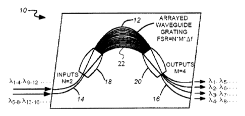
Figure 2 shows an illustrative embodiment of a multiplexer / demultiplexer
device 10
according to the invention, including an arrayed waveguide grating 12
comprising a
plurality of unequal length waveguides, a plurality of input waveguides 14, a
plurality of
output waveguides 16, and first and second planar waveguides 18 and 20,
respectively.
The entire device may be integrated on the same substrate chip using known
techniques.
The first and second planar waveguides 18 and 20 are interconnected by an AWG
12 in
which the lengths of adjacent waveguides 22 differ by a constant value and
increase
geometrically from one side to the other, as provided for in the design. This
structure
produces an output response that is periodic in frequency.
The periodic response can be described as the free spectral i-ange (FSR) of
the device.
The FSR is shown as a frequency period in Fig. 3 as 800 GHz. In order to
design a
multiplexer / demultiplexer suitable for all sub-bands in a wavelength range
of interest,
the FSR should, one would assume, be limited to frequency range to incorporate
one sub-
band of channels, for example for a four channel system an FSR=400 GHz. Then
with
only one input 14, the periodicity (FSR) will cause each channel of a sub-band
to be
demultiplexed to an output 16 of the device 10, at different orders of the
grating for evet-y
sub-band. However, high losses in the range of 3 dB attributed as roll-off
would be
experienced in such a system. The FSR defines a maximum power envelope that
has a
normally Gaussian shape between zero loss and -3 dB. The Gaussian envelope is
illustrated as 30 in Fig. 4, as designed for an example of the present
invention. The
smaller the FSR, the smaller the envelope, and consequently fewer channels can
be
passed in the low loss portion of the envelope.
The present invention has found that the FSR can be broadened to permit more
channels
to pass within the low loss portion of the envelope, to reduce roll-off
losses, if the number
of inputs is increased. An output response, as illustrated in Figs. 3 and 4,
results having
complementary output sub-bands from each input passed under a broader 800 GHz
envelope, as shown in Fig. 4. When the number of inputs is greater than one,
input roll-
off must also be factored into optimizing calculations. In the example shown
in Figs. 2-4,
channel bands of four channels are selected, thus the device 10 has 4 outputs
16. By
5
CA 02328696 2001-09-07
Doc. No. 10-424 CA Patent
optimizing input and output roll-off an optimum number of 2 inputs 14 is
selected.
Calculations shown in Table 1 of expected roll-off losses for a 4 channel sub-
band
illustrate how this selection is made.
N M Input roll-off Output roll-off Total losses
1 4 0 1.63 1.63
8 0 2.15 2.15
16 0 2.45 2.45
2 4 .75 0.4 1.15
8 .75 0.6 1.35
16 .75 0.7 1.45
4 4 1.63 0.2 1.83
8 1.63 0.23 1.86
16 1.63 0.28 1.91
Table 1
As can be seen in the table, the AWG of the present example having 2 inputs
and 4
outputs has a calculated colnbined loss of only 1.15 dB, rather than the 1.63
dB losses of
a single input of a 400 GHz FSR grating.
To obtain a multiplexer / demultiplexer designed for all channels, the FSR
must be equal
to the number of inputs N times the number of outputs M times the channel
spacing Af,
where N and M ai-e greater than 1. Thus, FSR=N*M*Af. The N input sub-band
frequencies must have a spectral separation of M*Af and the M output channel
frequencies must have a spectral separation of Af. In the illustrated example,
N=2, M=4
and Af=IOOGHz, so the FSR= 800GHz. To achieve a spectral separation of M*Af at
the
inputs N the design must provide a selected physical separation between the
inputs 14
known from the dispersion relation between physical sepai-ation in a dispet-
sive element
and specti-al separation.
In order to configure the device 10 for a selected channel band, the correct
input 14 must
be selected. This can be done statically connecting the selected input
permanently upon
installation, or dynamically with a simple 1xN switch (not shown) in this case
1x2.
6
CA 02328696 2001-09-07
Doc. No. 10-424 CA Patent
There is a further en-or that must be compensated fot- in order to use a same
AWG device
effectively over the full range of channel bands. As is known in the art,
there are only
discrete values possible fot- an FSR of an arl-ayed waveguide grating. Accoi-
dingly, the
best FSR selected may not provide channel passbands exactly centered on the
ITU grid.
As a result, there is an increasing wavelength centering error of the channels
that
correspond to lower orders of the grating. The problem is graphically
illustrated in Fig.
5. Fig. 5 shows the wavelength centering error for a 56 channel system whet-e
N=2 and
M=4. Each of the linked channel sub-bands is distributed progressively farther
ft-om
zero displacement about the center wavelength bands. A further unavoidable
dispersion
error, shown in Fig. 5 as the diffei-ent slopes of the sub-bands, t-esults
from using different
grating orders which have different wavelength dispersions.
From Fig. 6 it can be seen that by providing a different tempei-atui-e set
point for each
sub-band, the sub-bands ai-e all brought to a centered position. The
individual set points
are obtained by heating the chip selectively for each sub-band using a tempei-
ature
controller (not shown). In the present example, a worst wavelength centering
ei-ror is
improved from 68 pm to18 pm when the AWG tempet-atut-e set point is adjusted
for each
sub-band. Other known techniques can also be used to correct the wavelength
centering
error, such as moving the input position or sti-essing the device.
It will be appreciated by those skilled in the art that while the invention
has been
desci-ibed and illustrated by an AWG, other dispersive elements having a
periodic
frequency spectrum could also be employed. Bulk optical devices such as
diffraction
gratings and holographic gratings can be used.
7