Note: Descriptions are shown in the official language in which they were submitted.
CA 02328697 2000-12-15
Doc. No. 10-406 CA Patent
DOUBLE-PASS FOLDED INTERLEAVER/DEINTERLEAVERS
FIELD OF THE INVENTION
The invention relates to optical devices. More particularly, the invention
relates to an
interleaver/deinterleaver having a folded design such that an optical signal
passes through a
single crystal multiple times.
BACKGROUND OF THE INVENTION
As telecommunications usage increases as a result of, for example, increased
Internet
usage, increased types of communications, population growth,
telecommunications providers are
required to provide greater voice- and data-carrying capacity. In order to
reduce cost and the
amount of time required to provide the increased capacity wavelength division
multiplexing
(WDM) and dense wavelength division multiplexing (DWDM) have been developed,
which
provide increased capacity without requiring new fiber optic cables.
WDM and DWDM technologies combine multiple optical signals into a single fiber
by
transporting different signals on a different optical wavelengths or channels.
Interleaving and
deinterleaving of optical channels is typically accomplished with thin film
optical filters.
However, multiple layers of film are required to interleave and deinterleave
multiple channels,
which increases the cost and complexity of a component. Another disadvantage
of multiple
layers of thin film for filtering is that the thin films break down over time,
especially when
operating under high power conditions.
What is needed is an improved optical device for use with WDM and/or DWDM
optical
signals.
SUMMARY OF THE INVENTION
Double-pass folded interleaver/deinterleavers are described. The device
includes a
birefringent assembly and multiple reflective elements. The reflective
elements reflect an optical
signal such that the optical signal follows a path that makes multiple passes
through the
birefringent assembly. The optical signal traverses the path twice before
being separated into a
first subset and a second subset directed to a second port and a third port,
respectively. Optical
1
CA 02328697 2000-12-15
Doc. No. 10-406 CA Patent
signals received via the second and the third port are combined into a
superset and directed to the
first port.
In one embodiment, a set of half wave plates are positioned between one or
more of the
reflective elements and the birefringint assembly. The half wave plates are
oriented with azimuth
angles such that the first subset of optical signals include even
International Telecommunications
Union (ITU) channels and the second set of optical channels includes odd ITU
channels.
BRIEF DESCRIPTION OF THE DRAWINGS
The invention is illustrated by way of example, and not by way of limitation
in the figures
of the accompanying drawings in which like reference numerals refer to similar
elements.
Figure 1 is a conceptual illustration of a conversion from an optical channel
scheme
having 100 GHz spacing to an optical channel scheme having 200 GHz.
Figure 2 is a block diagram of an optical deinterleaver for conversion from an
optical
channel scheme having 50 GHz spacing to an optical channel scheme having 200
GHz spacing.
Figure 3 is a block diagram of an optical interleaver for conversion from an
optical
channel scheme having 200 GHz spacing to an optical channel scheme having 50
GHz spacing.
Figure 4a illustrates a top view of one embodiment of a double-pass folded
interleaver/deinterleaver.
Figure 4b illustrates a top view of one embodiment of a double-pass folded
interleaver/deinterleaver.
Figure 4c illustrates a top view of one embodiment of a double-pass folded
interleaver/deinterleaver.
Figure 5 illustrates a side view of one embodiment of the double-pass folded
interleaver/deinterleaver of Figure 4
Figure 6 illustrates a cross-sectional view of polarization states of a double-
pass optical
interleaver/deinterleaver as illustrated in Figures 4 and 5.
2
CA 02328697 2000-12-15
Doc. No. 10-406 CA Patent
Figure 7a illustrates a top view of a mufti-pass optical
interleaver/deinterleaver.
Figure 7b illustrates a side view of the mufti-pass optical
interleaver/deinterleaver of
Figure 8a.
Figure 8a illustrates a top view of one embodiment of a double-pass folded
interleaver/deinterleaver.
Figure 8b illustrates a top view of one embodiment of a double-pass folded
interleaver/deinterleaver.
Figure 8c illustrates a top view of one embodiment of a double-pass folded
interleaver/deinterleaver.
Figure 9 illustrates one embodiment of an optical interleaver/deinterleaver
having two
birefringent assemblies.
DETAILED DESCRIPTION
Double-pass folded interleaver/deinterleavers are described. In the following
description,
for purposes of explanation, numerous specific details are set forth in order
to provide a thorough
understanding of the invention. It will be apparent, however, to one killed in
the art that the
invention can be practiced without these specific details. In other instances,
structures and
devices are shown in block diagram form in order to avoid obscuring the
invention.
Reference in the specification to "one embodiment" or "an embodiment" means
that a
particular feature, structure, or characteristic described in connection with
the embodiment is
included in at least one embodiment of the invention. The appearances of the
phrase "in one
embodiment" in various places in the specification are not necessarily all
referring to the same
embodiment.
Interleaver/deinterleaver apparatuses for combining/separating optical
channels are
described. An interleaver/deinterleaver apparatus is described as folded when
an optical signal
follows an optical path that passes through a birefringent assembly multiple
times. Double-pass
refers to the optical signal following a (folded) path through the
birefringent assembly twice.
3
CA 02328697 2000-12-15
Doc. No. 10-406 CA Patent
When operating as an deinterleaver, the interleaver/deinterleaver separates an
optical signal (e.g.,
WDM signal) into subsets of optical signals (e.g., channels). In one
embodiment, deinterleaving
optical signals separates an optical signal into even and odd International
Telecommunications
Union (ITU) channels.
When operating as an interleaver, the interleaver/deinterleaver mixes subsets
of optical
signals (e.g., channels) into a multiplexed (e.g., WDM) optical signal. The
interleaver/deinterleaver apparatus can be used to increase the bandwidth of
an optical network.
For example, the interleaver/de-interleaver can be used to interface
components designed for a
first channel spacing (e.g., 100 GHz) to components designed for a second
channel spacing (e.g.,
200 GHz). In one embodiment, interleaveing combines even and odd ITU channels
into a single
optical signal.
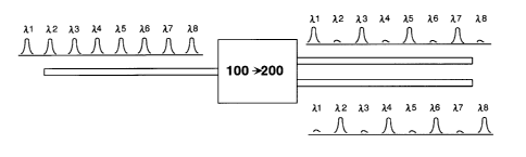
Figure 1 is a conceptual illustration of a conversion from an optical channel
scheme
having 100 GHz spacing to an optical channel scheme having 200 GHz. The
conversion of
Figure 1 is useful, for example, to allow devices designed to operate with an
optical channel
scheme having 200 GHz channel spacing to interact with other devices or a
network designed to
operate with an optical channel scheme having 100 GHz channel spacing.
Conversion between
100 GHz channel spacing and 200 GHz channel spacing allows, for example,
network bandwidth
to be increased without upgrading all of the devices that interact with the
network.
In one embodiment, the converter of Figure 1 is a deinterleaver that separates
an optical
signal having even and odd channels (e.g., ITU channels) into a first optical
signal including the
even channels and a second optical signal including the odd signals. After the
signals are
deinterleaved, the odd channels have a 200 GHz spacing and the even channels
have a 200 GHz
spacing. Recombining the even and the odd channels can be accomplished with an
interleaver
that combines the odd channels and the even channels into a single optical
signal. In other
words, the even and odd channels having 200 GHz spacing are combined
(interleaved) into an
optical signal having 100 GHz signal spacing. Similar interleaving can be
provided to convert
between 50 GHz spaced channels and 100 GHz spaced channels, as well as between
other sets of
channel spacing schemes.
Figure 2 is a block diagram of an optical deinterleaver for conversion from an
optical
channel scheme having 50 GHz spacing to an optical channel scheme having 200
GHz spacing.
4
CA 02328697 2000-12-15
Doc. No. 10-406 CA Patent
In general, deinterleaver 200 includes deinterleaver 210 to convert from one
set of 50 GHz
spaced channels to two sets of 100 GHz spaced channels. Deinterleaver 200 also
includes two
deinterleavers (220 and 230) each of which convert one of the sets of 100 GHz
spaced channels
to two sets of 200 GHz spaced channels. Deinterleaver 200 allows devices
designed for 200
GHz spaced channels to interact with devices or networks designed for 50 GHz
spaced channels.
Optical fiber 205 carries a set of optical channels, i , having 50 GHz
spacing.
Deinterleaver 210 separates the set of optical channels into sets of even, 2~j
+1~, and odd,
2 j + 1, channels. The even channels are input to deinterleaver 230 and the
odd channels are
input deinterleaver 220. The even and the odd channels have 100 GHz spacing.
Deinterleavers 220 and 230 operate to further separate the set of optical
channels.
Conceptually, deinterleaver 220 and 230 operate on the respective 100 GHz
spaced channels to
separate the input channels into "even" and "odd" channels. The sets of
channels output by
deinterleavers 220 and 230 have 200 GHz spacing.
Deinterleaver 220 separates the odd channels into two sets of channels, odd-
odd channels,
4k + 1, output by optical fiber 240 and odd-even, 4k + 2 , channels output by
optical fiber 250.
Deinterleaver 230 separates the even channels into two sets of channels, the
even-odd, 4k + 3 ,
channels output by optical fiber 260 and the even-even, 4~k + 1~ , channels
output by optical fiber
270.
The four sets of channels output by deinterleaver 200 are 200 GHz spaced
channels.
Thus, deinterleaver 200 can be used to interface one or more devices designed
to operate on 200
GHz spaced channels with one or more devices or networks designed to operate
on 50 GHz
spaced channels. Other channel spacings can also be supported.
Figure 3 is a block diagram of an optical interleaver for conversion from an
optical
channel scheme having 200 GHz spacing to an optical channel scheme having 50
GHz spacing.
In general, interleaver 300 includes interleaver 310 to convert from two sets
of 200 GHz spaced
channels to one set of 100 GHz spaced channels. Similarly, interleaver 320
converts from two
sets of 200 GHz spaced channels to one set of 100 GHz channels. Interleaver
330 converts the
two sets of 100 GHz spaced channels to one set of 50 GHz spaced channels.
Interleaver 300
allows devices designed for 200 GHz spaced channels to interact with devices
or networks
designed for 50 GHz spaced channels.
5
CA 02328697 2000-12-15
Doc. No. 10-406 CA Patent
The odd-odd, 4k + 1, channels having 200 GHz spacing are input to interleaves
310 via
optical fiber 340. The odd-even, 4k + 2 , channels having 200 GHz spacing are
input to
interleaves 310 via optical fiber 350. Interleaves 310 interleaves the odd-odd
channels and the
odd-even channels to generate a set of odd, 2 j + 1, channels having 100 GHz
spacing.
The even-odd, 4k + 3 , channels having 200 GHz spacing are input to
interleaves 320 via
optical fiber 360. The even-even, 4~k + 1) , channels having 200 GHz spacing
are input to
interleaves 320 via optical fiber 370. Interleaves 320 interleaves the even-
odd channels and the
even-even channels to generate a set of even, 2~j +1), channels having 100 GHz
spacing.
Interleaves 330 interleaves the even and odd channels to generate a set of
channels, i ,
having 50 GHz spacing. Thus, interleaves 300 allows devices designed to
operate on optical
channels having 200 GHz spacing to interact with devices designed to operate
on optical
channels having 50 GHz spacing. Other channels spacings can also be supported.
Figure 4a illustrates a top view of one embodiment of a double-pass folded
interleaver/deinterleaver. The arrows of Figure 4a correspond to the double-
pass folded
interleaver/deinterleaver operating as a deinterleaver. In other words an
optical signal carrying
information on multiple frequencies, for example, a wavelength division
multiplexed (WDM)
signal is receives and separated into two optical signals, each of which
include a predetermined
subset of frequencies (e.g., even channels and odd channels) from the input
optical signal.
An optical signal is received through port 400. In one embodiment, port 400 is
a
collimator assembly having a GRIN lens to collimate the light and a walk-off
crystal to separate
the horizontally polarized and the vertically polarized components of the
optical signal. Other
types of lenses can also be used, or pre-collimated light can be received.
Port 400 receives an
optical signal via an optical fiber and collimates the optical signal with the
GRIN lens.
In one embodiment, port 400 also includes half wave plate 402 to rotate either
the
vertically polarized component or the horizontally polarized component of the
optical signal. In
one embodiment, half wave plate 402 has an azimuth angle of 45° with
respect to an optical
signal received by port 400 from optical fiber 404. In one embodiment, the
walk-off crystal of
port 400 offsets the vertically polarized component of the optical signal and
half wave plate 402
causes the vertically polarized component to be horizontally polarized such
that both components
are horizontally polarized when the components pass through polarizes 405.
6
CA 02328697 2000-12-15
Doc. No. 10-406 CA Patent
The collimated optical signal is directed to polarizer 405 through a small
opening
between walk-off crystal 480 and walk-off crystal 482. In one embodiment,
polarizer 405
provides polarization in the range of 0° to 15° (e.g.,
2.6°) for optical signals passing from port
400 to birefringent assembly 420, however, other polarizations can be provided
based on, for
example, the azimuth angles of one or more half wave plates.
The polarized optical signal is then passed through half wave plate 410. In
one
embodiment, half wave plate 410 is oriented with a first predetermined azimuth
angle. In one
embodiment, the first azimuth angle is in the range of 0° to -
15° (e.g., -6.5°) for optical signals
passing from port 400 to birefringent assembly 420; however, the azimuth angle
can be different
with appropriate changes to the azimuth angles of one or more other half wave
plates and/or
polarizer 405. Half wave plate 410 introduces a relative phase difference of
180° between the
ordinary and extraordinary components of the optical signal.
After passing through half wave plate 410, the optical signal is directed to
birefringent
assembly 420. In one embodiment, birefringent assembly 420 is composed of
crystals 424 and
426 that are selected to provide improved thermal stability over a range of
operating temperatures
as compared to a single birefringent crystal. In one embodiment, crystal 424
is a Ti02 crystal
having a thickness of 2 mm, and crystal 426 is a YV04 crystal having a
thickness of 9.5 mm;
however, other sizes can also be used. Other birefringent assemblies can also
be used, for
example, a single crystal can be used if temperature stability is not
important, or other two-crystal
birefringent assemblies can be used.
After passing through birefringent assembly 420, the optical signal passes
through half
wave plate 430. In one embodiment, half wave plate 430 is oriented with the an
azimuth angle in
the range of 0° to -15° (e.g., -6.5°) for optical signals
passing from birefringent assembly 420 to
reflective element 450. Other azimuth angles for half wave plate 430 or for
both half wave plate
430 and half wave plate 410 can be used for different filtering
characteristics or physical
configurations.
After passing through half wave plate 430, the optical signal is reflected by
reflective
element 450. In one embodiment, reflective element 450 is a 90°
reflecting crystal; however,
other reflective elements can be used based on, for example, the physical
layout of the
interleaver/deinterleaver. In one embodiment, the faces) through which the
optical signal is
7
CA 02328697 2000-12-15
Doc. No. 10-406 CA Patent
received and/or reflected has low-order compensator 440 component to
compensate for phase
shift in the respective crystals. If the reflective element does not cause a
phase shift, low-order
compensator 440 can be omitted.
The optical signal reflected by reflective element 450 is directed through
half wave plate
432. Half wave plate 432 introduces a relative phase difference of 180°
between the ordinary
and extraordinary waves of the optical signal. In one embodiment, half wave
plate 432 is
oriented with a second predetermined azimuth angle. In one embodiment, the
second azimuth
angle is in the range of 15° to 30° (e.g., 22.5°) for
optical signals passing from reflective element
450 to birefringent assembly 420; however, the azimuth angle can be different
with appropriate
changes to the angles of one or more other half wave plates.
The optical signal passes through birefringent assembly 420 to reflective
element 452.
The optical signal is reflected by reflective element 452 back through
birefringent assembly 420.
In one embodiment, reflective element 452 is a 90° reflecting crystal;
however, other reflective
elements can be used. In one embodiment, the faces) through which the optical
signal is
received and/or reflected has low-order compensator 442 to compensate for
phase shift in the
respective crystals. If the reflective element does not cause a phase shift,
low-order compensator
442 can be omitted.
After passing through birefringent assembly 420 as reflected by reflective
element 452,
the optical signal passes through half wave plate 434. In one embodiment, half
wave plate 434
has an azimuth angle is in the range of 15° to 30° (e.g.,
22.5°) for optical signals passing from to
birefringent assembly 420 to walk-off crystal 460. Other azimuth angles for
half wave plate 434
can be used for different filtering characteristics or physical
configurations.
When the optical signal is traveling from birefringent assembly 420, the
optical signal
passes between half wave plates 436a and 436b. One configuration for half wave
plates 436a
and 436b is described in greater detail below with respect to Figure 5. In one
embodiment, the
azimuth angle of half wave plates 436a and 436b are in the range of 40°
to 50° (e.g., 45°) for
optical signals passing from walk-off crystal 460 to birefringent assembly
420; however, the
azimuth angle can be different with appropriate changes to the azimuth angles
of one or more
other half wave plates and/or polarizer 405.
CA 02328697 2000-12-15
Doc. No. 10-406 CA Patent
The optical signals pass through half wave plate 470 and are reflected by
quarter wave
mirror 472. In one embodiment, the azimuth angle of half wave plate 470 is in
the range of 40°
to 50° (e.g., 45°) for optical signals passing from walk-off
crystal 460 to quarter wave mirror
472; however, the azimuth angle can be different with appropriate changes to
the azimuth angles
of one or more other half wave plates and/or polarizes 405. The effect of walk-
off crystal 460 is
described in greater detail below with respect to Figure 5. Quarter wave
mirror 472 reflects the
optical signals back through walk off crystal 460. Quarter wave mirror 472
also introduces a
relative phase shift of 90° between the ordinary and extraordinary
components of the optical
signal.
After passing through half wave plates 436a and 436b, the optical signals pass
through
birefringent assembly 420 and are reflected by reflective element 452 through
birefringent
assembly 420 through half wave plate 432 to reflective element 450. Reflective
element 450
reflects the signals through half wave plate 430, birefringent assembly 420,
half wave plate 410
and polarizes 405 to walk-off crystals 480 and 482. Walk-off crystals 480 and
482 direct the
optical signals to ports 490 and 492, respectively.
Port 490 includes half wave plate 496 and port 492 includes half wave plate
494. In one
embodiment, both half wave plate 494 and half wave plate 496 have azimuth
angles of 45° with
respect to optical signals received from walk-off crystal 482 and walk-off
crystal 480,
respectively. Half wave plate 494 and 496 rotate the optical components
received such that ports
492 and 490, respectively, each receive a vertically polarized component and a
horizontally
polarized component, which are combined and directed to optical fibers 493 and
495,
respectively.
To operate as an interleaves, two sets of optical signals are input to ports
490 and 492.
The two sets of optical signals are combined in a manner that is the reverse
of the deinterleaver
function described above. The combined (interleaved) optical signal is output
through port 400.
Thus, the apparatus illustrated in Figure 4 can operate as an interleaves or
as a deinterleaver.
In one embodiment, the interleaver/deinterleaver of Figure 4a is angle tuned
to
compensate for manufacturing tolerances. In one embodiment, angle tuning is
accomplished by
rotating birefringent assembly 420 after the interleaver/deinterleaver has
been assembled so that
the signals (e.g., ITU channels) interleaved or deinterleaved match the
desired characteristics.
9
CA 02328697 2000-12-15
Doc. No. 10-406 CA Patent
Birefringent assembly 420 is rotated to increase the optical path length of
the signals passing
through birefringent assembly 420. When the desired optical path length is
provided,
birefringent assembly 420 is maintained in the desired position through, for
example, use of
epoxy or soldering techniques.
Figure 4b illustrates a top view of one embodiment of a double-pass folded
interleaver/deinterleaver. The interleaver/deinterleaver of Figure 4b includes
the same
components (e.g., reflective elements, half wave plates, birefringent
assembly) as the
interleaver/deinterleaver of Figure 4a; however, the components are arranged
in different
physical positions for the interleaver/deinterleaver of Figure 4b compared to
the
interleaver/deinterleaver of Figure 4a.
In one embodiment, the interleaver/deinterleaver of Figure 4b does not include
the low-
order compensators of the interleaver/deinterleaver of Figure 4a. The optical
compensation of
the low-order compensators can be provided by angle tuning birefringent
assembly 420. The
increase optical path length through material of the interleaver/deinterleaver
can be provided by
birefringent assembly 420 rather than by the low-order compensators. In an
alternate
embodiment, the interleaver/deinterleaver of Figure 4b can include low-order
compensators as
described above with respect to Figure 4a.
Figure 4c illustrates a top view of one embodiment of a double-pass folded
interleaver/deinterleaver. The interleaver/deinterleaver of Figure 4c includes
the same
components (e.g., reflective elements, half wave plates, birefringent
assembly) as the
interleaver/deinterleaver of Figures 4a and 4b with the addition of reflective
element 454. The
components are arranged in different physical positions for the
interleaver/deinter-leaver of
Figure 4c compared to the interleaver/deinterleaver of Figures 4a and 4b.
In one embodiment, the interleaver/deinterleaver of Figure 4c does not include
the low-
order compensators of the interleaver/deinterleaver of Figure 4a. The optical
compensation of
the low-order compensators can be provided by angle tuning birefringent
assembly 420. The
increase optical path length through material of the interleaver/deinterleaver
can be provided by
birefringent assembly 420 rather than by the low-order compensators. In an
alternate
embodiment, the interleaver/deinterleaver of Figure 4b can include low-order
compensators as
described above with respect to Figure 4a.
CA 02328697 2000-12-15
Doc. No. 10-406 CA Patent
Figure 5 illustrates a side view of one embodiment of the double-pass folded
interleaver/deinterleaver of Figures 4a and 4b. The side view of Figure 5 is
from the side of port
490 and walk-off crystal 460.
When operating as a deinterleaver, the optical signal input to the
interleaver/de-
interleaves travels to half wave plate 434 and walk-off crystal 460 as
described above with
respect to Figures 4a and 4b. Walk-off crystal 460 offsets the optical signals
such that when the
optical signals are reflected, one set of optical signals passes through half
wave plate 436a and
the second set of optical signals passes through half wave plate 436b. The
polarization states of
the optical signals is described in greater detail below.
The two optical signals are reflected back to walk-off crystal 480 and walk-
off crystal 482
as described above. Walk-off crystal 480 and walk-off crystal 482 shift the
optical signals to be
aligned with ports 490 and 492. The signals are output through ports 490 and
492.
To operate as an interleaves, two sets of optical signals are input to ports
490 and 492.
The two sets of optical signals are combined in a manner that is the reverse
of the deinterleaver
function described above. The combined (interleaved) optical signal is output
through port 400.
Thus, the apparatus illustrated in Figure 4 can operate as an interleaves or
as a deinterleaver.
Figure 6 illustrates a cross-sectional view of polarization states of a double-
pass optical
interleaver/deinterleaver as illustrated in Figures 4a and 5. With respect to
Figure 6, a forward
pass cross-sectional view refers to an illustration of the polarization states
of one or more optical
signals as the signals) pass from the input ports) to quarter wave mirror 472.
A backward pass
cross-sectional view refers to an illustration of the polarization states of
one or more signals as
the signals) pass from quarter wave mirror 472 to the output port(s).
State 600 represents the input/output ports 400, 490 and 492 of Figures 4 and
5 having
input/output signals 600, 690 and 692, respectively. The input and output port
receive and send,
respectively, optical signals having both horizontal and vertical components.
The arrows of
Figure 6 indicate the polarization state sequence for a deinterleaver.
State 610 is the forward pass cross-sectional view of input optical signal 680
between
walk-off crystals 480 and 482 and polarizes 405. In one embodiment, input port
400 includes a
walk-off crystal to separate the input signal into two sub-beams and a half
wave plate to rotate
one of the sub-beams 90°.
11
CA 02328697 2000-12-15
Doc. No. 10-406 CA Patent
State 620 is the forward pass cross-sectional view of output optical signals
690 and 692
between 420 and 434. In state 620 output optical signal 690 has two vertically
polarized
components and output optical signal 692 has two horizontally polarized
components.
State 630 is the forward pass cross-sectional view of the output optical
signal 690 and
692 between walk-off crystal 460 and half wave plate 470. In state 630, the
vertical components
of output optical signal 690 have been shifted by walk off crystal 460. The
dashed lines shown
in state 630 represent the position of half wave plates 436a and 436b.
State 640 is the backward pass cross-sectional view of output optical signals
690 and 692
between 470 and 460. In state 640 both components of both output optical
signals have been
rotated 90° by quarter wave mirror 472.
State 650 is the backward pass cross-sectional view of output optical signals
690 and 692
between 434 and 420. Both components of output optical signal 692 have been
shifted by walk-
off crystal 460 and both components of both output optical signals 690 and 692
have been rotated
by half wave plates 436a and 436b.
State 660 is the backward pass cross-sectional view of output optical signals
690 and 692
between polarizer 405 and walk-off crystals 480 and 482. Both output optical
signals 690 and
692 have two horizontally polarized components that are aligned with walk-off
crystals 480 and
482 respectively.
State 670 is the backward pass cross-sectional view of output optical signals
690 and 692
between walk-off crystals 480 and 482 and ports 492 and 490. Walk-off crystals
480 and 482
provide offset to align output optical signals 680 and 682 with ports 490 and
492, respectively.
Figure 7a illustrates a top view of one embodiment of a mufti-pass optical
interleaver/deinterleaver. In the mufti-pass optical interleaver/deinterleaver
of Figure 7a, the
optical signals make the first pass through the interleaver/deinterleaver to
quarter wave mirror
472 in the same manner as with the interleaver/deinterleaver of Figure 4.
Quarter wave mirror 472 reflects the signals back thorough birefringent
assembly 420 in
the same manner as the interleaver/deinterleaver of Figure 4 except that
rather than being
received and offset by walk off crystals 480 and 482, the optical signals pass
through half wave
plate 410 and polarizer 405 reflected by quarter wave mirror 780. Quarter wave
mirror 780, and
half wave plates 780 and 782 rotate the optical signals. The optical signals
are reflected back
12
CA 02328697 2000-12-15
Doc. No. 10-406 CA Patent
through birefringent assembly 420 in a similar manner as described above
through half wave
plate 734 to ports 790 and 792.
Ports 790/792 (port 792 is behind port 790 and therefore obscured in the
illustration of
Figure 7a) include half wave plates 792/794, respectively. In one embodiment,
both half wave
plate 792 and half wave plate 794 have azimuth angles of 45° with
respect to optical signals
received from walk-off crystal 460. Half wave plates 792 and 794 rotate the
optical components
received such that ports 792 and 790, respectively, each receive a vertically
polarized component
and a horizontally polarized component, which are combined and directed to
optical fibers.
To operate as an interleaver, two sets of optical signals are input to ports
790 and 792.
The two sets of optical signals are combined in a manner that is the reverse
of the deinterleaver
function described above. The combined (interleaved) optical signal is output
through port 700.
Thus, the apparatus illustrated in Figure 7a can operate as an interleaver or
as a deinterleaver.
In one embodiment, the interleaver/deinterleaver of Figure 7a is angle tuned
to
compensate for manufacturing tolerances. In one embodiment, angle tuning is
accomplished by
rotating birefringent assembly 420 after the interleaver/deinterleaver has
been assembled so that
the signals (e.g., ITU channels) interleaved or deinterleaved match the
desired characteristics.
Birefringent assembly 420 is rotated to increase the optical path length of
the signals passing
through birefringent assembly 420. When the desired optical path length is
provided,
birefringent assembly 420 is maintained in the desired position through, for
example, use of
epoxy or soldering techniques.
Figure 7b illustrates a side view of the multi-pass optical
interleaver/deinter-leaver of
Figure 7a. As mentioned above, the optical signals make the first pass through
the
interleaver/deinterleaver to quarter wave mirror 472 in the same manner as
with the
interleaver/deinterleaver of Figure 4.
Walk-off crystals 785 and 787 offset the optical signals and quarter wave
mirrors 780
reflect the optical signals back through birefringent assembly 420 as
described above. The
optical signals are reflected back through birefringent assembly 420 in a
similar manner as
described above to walk-off crystals 780 an 785, which offset optical signals
to ports 790 and
792, respectively.
13
CA 02328697 2000-12-15
Doc. No. 10-406 CA Patent
Figure 8a illustrates a top view of one embodiment of a double-pass folded
interleaver/deinterleaver. The interleaver/deinterleaver of Figure 8a includes
the same
components (e.g., reflective elements, half wave plates, birefringent
assembly) as the
interleaver/deinterleaver of Figure 4a with the addition of reflective
elements 800 and 810 and
half wave plates 433 and 435. In one embodiment, half wave plate 433 has an
azimuth angle of
22.5° for optical signals passing form reflective element 450 to
birefringent assembly 420 and
half wave plate 435 has an azimuth angle of 22.5° for optical signals
passing from reflective
element 800 to birefringent assembly 420.
In one embodiment, the components are arranged in different physical positions
for the
interleaver/deinterleaver of Figure 8a compared to the
interleaver/deinterleaver of Figure 4a to
provide similar functionality. The interleaver/deinterleaver of Figure 8a
provides improved
filtering as compared to Figure 4a because optical signals are passed through
birefringent
assembly 420 a greater number of times.
In one embodiment, the interleaver/deinterleaver of Figure 8a does not include
the low-
order compensators of the interleaver/deinterleaver of Figure 4a. The optical
compensation of
the low-order compensators can be provided by angle tuning birefringent
assembly 420. The
increase optical path length through material of the interleaver/deinterleaver
can be provided by
birefringent assembly 420 rather than by the low-order compensators. In an
alternate
embodiment, the interleaver/deinterleaver of Figure 8a can include low-order
compensators as
described above with respect to Figure 4a.
Figure 8b illustrates a top view of one embodiment of a double-pass folded
interleaver/deinterleaver. The interleaver/deinterleaver of Figure 8b includes
the same
components (e.g., reflective elements, half wave plates, birefringent
assembly) as the
interleaver/deinterleaver of Figure 8a; however, the components are arranged
in different
physical positions for the interleaver/deinterleaver of Figure 8b compared to
the
interleaver/deinterleaver of Figure 8a.
In one embodiment, the interleaver/deinterleaver of Figure 8b does not include
the low-
order compensators. The optical compensation of the low-order compensators can
be provided
by angle tuning birefringent assembly 420. The increase optical path length
through material of
the interleaver/deinterleaver can be provided by birefringent assembly 420
rather than by the low-
14
CA 02328697 2000-12-15
Doc. No. 10-406 CA Patent
order compensators. In an alternate embodiment, the interleaver/deinterleaver
of Figure 8b can
include low-order compensators as described above with respect to Figure 4a.
Figure 8c illustrates a top view of one embodiment of a double-pass folded
interleaver/deinterleaver. The interleaver/deinterleaver of Figure 8c includes
the same
components (e.g., reflective elements, half wave plates, birefringent
assembly) as the
interleaver/deinterleaver of Figure 8a with the addition of reflective element
820. In one
embodiment, the components are arranged in different physical positions for
the
interleaver/deinterleaver of Figure 8c compared to the
interleaver/deinterleaver of Figure 4a to
provide similar functionality.
In one embodiment, the interleaver/deinterleaver of Figure 8c does not include
the low-
order compensators. The optical compensation of the low-order compensators can
be provided
by angle tuning birefringent assembly 420. The increase optical path length
through material of
the interleaver/deinterleaver can be provided by birefringent assembly 420
rather than by the low-
order compensators. In an alternate embodiment, the interleaver/deinterleaver
of Figure 8c can
include low-order compensators as described above with respect to Figure 4a.
Figure 9 illustrates one embodiment of an optical interleaver/deinterleaver
having two
birefringent assemblies. The interleaver/deinterleaver of Figure 9 includes
the same components
(e.g., reflective elements, half wave plates, birefringent assembly) as the
interleaver/deinterleaver
of Figure 4a with the addition of brirefringent assembly 920, which includes,
in one embodiment,
crystals 924 and 926. The interleaver/de-interleaver of Figure 9 provides
improved filtering as
compared to Figure 4a because optical signals are passed through birefringent
assembly 420 and
through birefringent assembly 920.
In one embodiment, the interleaver/deinterleaver of Figure 9a does not include
the low
order compensators of the interleaver/deinterleaver of Figure 4a. The optical
compensation of
the low-order compensators can be provided by angle tuning birefringent
assembly 420 and/or
birefringent assembly 920. The increase optical path length through material
of the
interleaver/deinterleaver can be provided by birefringent assembly 420 and/or
birefringent
assembly 920 rather than by the low-order compensators. In an alternate
embodiment, the
interleaver/deinterleaver of Figure 9 can include low-order compensators as
described above with
respect to Figure 4a.
CA 02328697 2000-12-15
Doc. No. 10-406 CA Patent
In the foregoing specification, the invention has been described with
reference to specific
embodiments thereof. It will, however, be evident that various modifications
and changes can be
made thereto without departing from the broader spirit and scope of the
invention. The
specification and drawings are, accordingly, to be regarded in an illustrative
rather than a
restrictive sense.
16