Note: Descriptions are shown in the official language in which they were submitted.
CA 02328759 2000-12-19
Doc. No 10-422 CA Patent
OPTICAL SWITCH
Field of the Invention
The present invention relates to the field of optical switches.
Background of the Invention
Optical matrix switches are commonly used in communications systems for
transmitting
voice, video and data signals. Generally, optical matrix switches include
multiple input
and/or output ports and have the ability to connect, for purposes of signal
transfer, any
input port/output port combination, and preferably, for N x M switching
applications, to
allow for multiple connections at one time. At each port, optical signals are
transmitted
and/or received via an end of an optical waveguide. The waveguide ends of the
input and
output ports are optically connected across a switch interface. In this
regard, for
example, the input and output waveguide ends can be physically located on
opposite
sides of a switch interface for direct or folded optical pathway communication
therebetween, in side-by-side matrices on the same physical side of a switch
interface
facing a mirror, or they can be interspersed in a single matrix arrangement
facing a
mirror.
Establishing a connection between a given input port and a given output port,
involves
configuring an optical pathway across the switch interface between the input
ports and
the output ports. One way to configure the optical pathway is by moving or
bending
optical fibers using, for example, piezoelectric benders.
Another way of configuring the optical path between an input port and an
output port
involves the use of one or more moveable mirrors interposed between the input
and
output ports. In this case, the waveguide ends remain stationary and the
mirrors are used
for switching. The mirrors can allow for two-dimensional targeting to
optically connect
any of the input port fibers to any of the output port fibers.
1
CA 02328759 2000-12-19
Doc. No 10-422 CA Patent
An important consideration in switch design is minimizing switch size for a
given
number of input and output ports that are serviced, i.e., increasing the
packing density of
ports and beam directing units. It has been recognized that greater packing
density can be
achieved, particularly in the case of a movable mirror-based beam directing
unit, by
folding the optical path between the fiber and the movable mirror and/or
between the
movable mirror and the switch interface. Such a compact optical matrix switch
is
disclosed in U.S. Patent No. 6,097,860. In addition, further compactness
advantages are
achieved therein by positioning control signal sources outside of the fiber
array and,
preferably, at positions within the folded optical path selected to reduce the
required size
of the optics path.
Current switch design continuously endeavors to provide smaller optical
switches.
However, in the current approach for optical switching between reflection
means, the
beam follows a "Z-shaped" path between the optical elements. Thus, by
providing an in-
line arrangement of the optical components a more compact optical switch can
be
provided.
It is an object of the present invention to provide an optical switch having
an in-line
arrangement of optical components.
It is an object of this invention to provide a more compact optical switch.
Another object of this invention is to provide a compact optical switch based
on
deflection means in transmission.
Summary of the Invention
3CI In accordance with the invention there is provided an optical switch
comprising: at least
one input port for launching a beam of light into the optical switch; at least
two output
2
CA 02328759 2000-12-19
Doc. No 10-422 CA Patent
ports for selectively receiving the beam of light from an optical path between
the at least
one input port and a selected one of the at least two output ports; a lens
having a focal
length approximately equal to the near zone length of the beam of light
incident thereon;
a first array of deflectors including a first fixed deflector and a first
plurality of
independently tiltable deflectors and a second array of deflectors including a
second fixed
deflector and a second plurality of independently tiltable deflectors, wherein
the first
fixed deflector is for receiving the beam of light from the at least one input
port via the
lens and for deflecting the beam of light to one of the second plurality of
independently
tiltable deflectors via the lens, and the second fixed deflector is for
receiving the beam of
light from one of the first plurality of independently tiltable deflectors via
the lens and for
deflecting the beam of light to a selected one of the at least two output
ports via the lens,
and wherein the first and the second plurality of independently tiltable
deflectors are for
switching the beam of light.
In accordance with the invention there is further provided an optical switch
comprising:
at least one input port for launching a beam of light into the optical switch;
at least two
output ports for selectively receiving the beam of light; a lens having a
focal length
approximately equal to the Raleigh range of the beam of light incident
thereon; a first
array of deflectors and a second array of deflectors for switching the beam of
light from
the at least one input port to a selected one of the at least two output ports
wherein the
switching is performed along an optical path including the first and the
second array of
deflectors and the lens and wherein the beam of light passes five times
through the lens
when switching the beam to a selected one of the at least two output ports.
Brief Description of the Drawings
Exemplary embodiments of the invention will now be described in conjunction
with the
drawings in which:
Fig. 1 is a schematic presentation of a prior art optical switch having a Z-
shaped
arrangement of optical components;
3
CA 02328759 2000-12-19
Doc. No 10-422 CA Patent
Fig. 2 shows a schematic presentation of an optical switch in accordance with
the present
invention;
Fig. 3 is a schematic presentation of an exemplary optical path for a beam of
light being
switched from an input port to a selected output port;
Fig. 4 shows a schematic presentation of a preferred embodiment of the optical
switch in
accordance with the present invention including a GRIN lens;
Fig. 5 shows a schematic presentation of an array of micro-mirrors provided on
a MEMS
chip;
Figs. 6a-6c show a schematic presentation of a Gaussian propagation of the
beam of light
through a GRIN lens when tilted by -7° (Fig. 6a), 0° (Fig. 6b)
and +7° (Fig. 6c); and
Fig. 7 shows a quintuple ATO switch in compat~ison to an "Astarte-like"
switch.
Detailed Description of the Invention
The present invention expands on the optical switch disclosed in CA X,XXX,XXX
(10-
384 CA and 10-412 CA). It develops the optical architecture of large optical
crossconnect structures and applies it to medium and small scale switches to
provide very
compact optical switches. For this purpose, a micro-mirror array of
independently 2D
tiltable micro-mirrors on a MEMS chip is used in conjunction with an angle-to-
offset
lens to provide a switch fabric in a miniaturized space. The waveguides or
fibers are fed
through the MEMS chips themselves for compactness, while a single common fixed
mirror is added on each opposite MEMS chip for targeting purpose.
Turning now to Fig. 1 a schematic presentation of a prior art optical switch
100 having a
Z-shaped arrangement of optical components is shown. A beam of light 102
enters the
switch and is reflected by a first fixed mirror 104 towards a first 2D mirror
106. The 2D
mirror 106 reflects beam 102 towards a second 2D mirror 108 which in turn
reflects
beam 102 to a second fixed mirror 110. The second fixed mirror 110 then
reflects beam
102 towards an output port 112. Fig. 1 clearly shows that beam 102 follows the
standard
3(1 Z-shaped approach for switching an optical signal. The Z-shape approach
requires
particular consideration with respect to the physical spacing between the
optical elements
4
CA 02328759 2000-12-19
Doc. No 10-422 CA Patent
since the beam of light should not be obstructed by some elements along the
optical path
through the switch. It is apparent that this is not a very efficient design.
As is seen, an array of 2 mirrors is used to steer the beam in transmission; a
first fixed
mirror is used to redirect the beam to a second 2D tiltable mirror that
provides beam
steering. In accordance with the present invention, each fixed mirror is
replaced with a
common mirror placed at the opposed focal planes of the ATO lens and share
this
common fixed mirror for every port. The optical switch in accordance with the
present
invention requires two common fixed mirrors, one for the input ports and one
for the
output ports. Such an arrangement allows to work with normal incidence on
mirrors
(reduced PDL) and provides a higher fill factor than prior art optical
switches, for
example a fill factor of close to SO% is achieved as in comparison to prior
art fill factors
of approximately 30%.
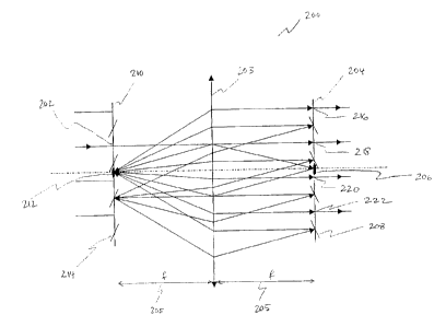
1S Fig. 2 shows a schematic presentation of an optical switch 200 in
accordance with the
present invention wherein the optical elements are arranged in-line. This
results in a
more compact design of optical switch 200. Switch 200 includes an input port
202, an
angle-to-offset (ATO) lens 203, a first array of deflectors 204 including a
first fixed
deflector 206 and a first plurality of 2D tiltable deflectors 208, a second
array of
deflectors 210 including a second fixed deflector 212 and a second plurality
of 2D tiltable
deflectors 214. The first and the second array of deflectors 204 and 210 can
be an array
of micro-mirrors tilting in two perpendicular directions and one fixed micro-
mirror. The
ATO lens 203 has a focal length 205 which corresponds to the near zone length
(multimode) or the Rayleigh range (single mode) of a beam of light incident
thereon. A
more detailed description of the ATO principle is provided below. The first
array of
deflectors 204 is arranged in a first focal plane of the ATO lens 203 and the
second array
of deflectors 210 is arranged in a second focal plane of the ATO lens 203. A
plurality of
output ports 216, 218, 220, and 222 is shown to be arranged on the first array
204.
Turning now to Fig. 3 a schematic presentation of an exemplary optical path
for a beam
of light being switched from an input port 302 to a selected output port 320
is shown, as
5
CA 02328759 2000-12-19
Doc. No 10-422 CA Patent
it travels through optical switch 300. A beam of light 301 is launched into
the optical
switch 300 at input port 302. Input port 302 is arranged on a second array of
deflectors/NIEMS chip 310. Beam 301 traverses through an ATO lens 303 and is
directed to a first fixed mirror 306 which is arranged on a first array of
deflectors/MEMS
chip 304. The first fixed mirror 306 then reflects beam 301 to an
independently 2D
tiltable micro-mirror 314 on MEMS chip 310 by going back through lens 303. As
is seen
from Fig. 3, beam 301 comes off at an angle when it is reflected by the first
fixed mirror
306 and from the lens 303 it is directed parallel to an optical axis until
beam 301 reaches
micro-mirror 314. Micro-mirror 314 is tilted to reflect beam 301 to micro-
mirror 308
which is arranged on the first MEMS chip 304 by going back through the lens
303.
Micro-mirror 308 sends the beam 301 back in parallel to the optical axis by
going
through lens 303 and then beam 301 collapses onto the second fixed mirror 312
arranged
on the second MEMS chip 310. The second fixed mirror 312 distributes beam 301
to
output port 320 by going through lens 303. It is apparent from Fig. 3 that
lens 303 is
used multiple times as beam 301 has traveled 5 times therethrough. This means
that lens
303 fulfils the function of a first telecentric relay, switching, and a second
telecentric
relay. By using a same lens multiple times a very compact optical switch is
provided.
However, in order to accomplish such a compact design, the input and output
ports are
provided directly on the second and first MEMS chip, respectively. The mirrors
and the
input/output ports share the available space on the MEMS chips and hence
optical
switches in accordance with the present invention have a low fill factor. As a
result of
the low fill factor and the maximum packing density on the MEMS chip, the
present
invention is used to provide very compact small scale switches, such as
compact 16x 16,
32x32, or 64x64 switches.
The present invention is also applicable to large optical
switches/crossconnects, but the
compactness advantage of having the coupling optics folded into the main
switch pass, as
opposed to the standard Z-shape approach, starts to be less attractive than
getting a higher
fill factor.
6
CA 02328759 2000-12-19
Doc. No l0-422 CA Patent
The input and output ports can consist of optical fibers coupled to collimator
lenses.
Depending on the material used for making the MEMS chip, the beam of light can
be
launched directly through a transparent region of the MEMS chip, i.e. a region
unobstructed by a micro-mirror, or a passage in form of a hole is provided on
the MEMS
chip to allow the beam of light to pass therethrough. If silicon or silica are
used as a
MEMS material, the light can be send directly through the MEMS chip since both
silicon
and silica are transparent in the infrared region, and in particular at 1.55
microns.
However, gallium arsenide (GaAs) or indium phosphide (InP) are preferred
materials for
photonic applications, e.g. lasers, detectors, etc., but they are not
transparent at 1.55
microns. In this case, a passage is provided on the MEMS to allow the beam of
light to
pass therethrough.
Fig. 4 shows a schematic presentation of a preferred embodiment of an optical
switch 400
in accordance with the present invention wherein the ATO lens is a GRIN lens
402. This
embodiment provides an even more compact optical switch. GRIN lens 402 is a'/a
pitch
SLW 3.0 SELFOCTM lens having a length of 7.89 mm. A 4x4 SMF input fiber bundle
404, is shown on the left of Fig. 4. It has a pitch of 250 pm. A micro-lens
array 406 is
disposed on the input fiber bundle 404 to expand the beams to an appropriate
diameter.
Exemplary dimensions of this micro-lens array 406 are a diameter of 125 pm, a
pitch of
250 pm, and an efl of 415 ~tm. A first array of micro-mirrors 408 including a
first
common fixed mirror and a first plurality of independently 2D tiltable micro-
mirrors is
disposed between the micro-lens array 406 and a first end face 410 of lens
402. The
dimension of the first array of micro-mirrors 408 is 125x125 ~m2, +/-
3.4°, +/- 0.2°. The
first end face 410 corresponds to a first focal plane of the lens 402. A
second end face
412 corresponding to a second focal plane is located on an opposed end face of
lens 402.
A second array of micro-mirrors 414 including a second common fixed mirror and
a
second plurality of independently 2D tiltable micro-mirrors is provided at the
second end
face 412. An output fiber bundle 418 having an array of micro-lenses 416
arranged
thereon is disposed at the second array of micro-mirrors 414. The first and
the second
array of micro-mirrors 408 and 414 are disposed on MEMS chips. These MEMS
chips
are mounted in the first and second focal plane of the GRIN lens 402, for
example by
7
CA 02328759 2000-12-19
Doc. No 10-422 CA Patent
gluing them to the lens 402. Since lens 402 is an ATO lens its focal length
corresponds
to the near zone length (multimode) or Rayleigh range (single mode) of a beam
light
incident thereon. The array of micro-mirrors 414, the array of micro-lenses
416, and the
SMF output fiber bundle have the same dimensions as the respective array of
micro-
s mirrors 408, the array of micro-lenses 406, and the SMF output fiber bundle
404 which
results in an overall dimension for optical switch 400 of 11 mm x 3 mm
diameter,
excluding the fiber bundles; a very compact optical switch. The total length
of the lens
402 corresponds to 2f, wherein f is the focal length of the lens.
Using a conventional GRIN lens, such as a SELFOCTM SLW 3.0 lens, as the main
optical
element allows to build a very compact switch and further potentially eases
the packaging
since conventional coupler-like assembly techniques can be used. The overall
footprint
for a 16x16 optical switch is less than 11 mm long and 3 mm in diameter
excluding the
fiber bundles, standard SMF28 on 250 pm pitch.
As was explained above, the beams of light can be launched through the MEMS
substrate
directly if it is made of silicon. However, for certain applications other
MEMS substrates
may be desired which are not transparent to the beams of light. In such a
case, a passage
or hole is provided on the substrate to allow the beams of light to pass
through the
2C1 MEMS chips.
In accordance with another embodiment of the present invention, the GRIN lens
402 is
foreshortened to create room for the optical components disposed at the
respective end
faces of the GRIN lens 402. A foreshortening of the GRIN lens maintains the
focal plane
of this lens but moves the lens away from the space of the focal plane to
accommodate
the array of micro-mirrors.
Fig. 5 shows a schematic presentation of an array of micro-mirrors provided on
a MEMS
chip 500 as disposed on a GRIN lens for example. A common fixed mirror 502 is
shown
in the center of Fig. 5. The fixed mirror 502 is surrounded by an array of 4x4
of
independently 2D tiltable micro-mirrors 504 and beams of light 506 are shown
in
8
CA 02328759 2000-12-19
Doc. No 10-422 CA Patent
between neighboring micro-mirrors 504. Exemplary dimensions of MEMS chip S00
are
presented in Fig. 5.
In the following a rough tolerancing example for optical switch 400 at 0.5 dB
extra loss is
presented. An overall insertion loss is smaller than 1 dB and is mainly due to
mirror
losses assuming 96% gold. The SELFOCTM usage is NA ~ 0.24 / SLW 3.0
recommended for NA < 0.46. Switch 400 has an insertion loss uniformity of ~
0.2 dB
which is mainly due to off-axis aberrations. A 1D look-up table is assumed.
The
position of the MEMS chip with respect to the SELFOCTM lens is +/- 8 microns.
Switch
400 has a pointing accuracy of +/- 0.25° or +/- 3.6% of range or +/-
7.2% of half-range.
The focal length of the micro-lenses is 415 pm and has a tolerance of +/- 16%.
The
length of the SELFOCTM lens is 7.89 mm and has a tolerance of +/-9%. It can be
polished to fit the MEMS chip if needed. The SMF fiber location with respect
to the
micro-lens array is +/- 1.8 pm. The parallelism of the SELFOCTM facets can be
compensated for by alignment of the MEMS chip with respect to the SELFOCTM
lens.
The architecture is scalable but a 16x 16 architecture is optimal for use with
the described
SELFOCTM lens. In summary, the design of optical switch 400 is very tolerant
as the
losses are very small, aberrations are very small, it has a very good loss
uniformity, a
simplified look-up table, the position of the MEMS chip with respect to the
lens is easy to
meet, it has a good pointing accuracy, the focal length is easy to meet.
Figs. 6a-6c show a schematic presentation of a Gaussian propagation of the
beam of light
through a GRIN lens when tilted by -7° (Fig. 6a), 0° (Fig. 6b)
and +7° (Fig. 6c). Figs. 6a
to 6c show that the GRIN lens is in agreement with the ATO lens principle in
that a
certain input mode is maintained at the output. For example, Fig. 6a shows
that when a
micro-mirror tilts a beam of light by -7° a negative position below the
optical axis is
reached at the opposed end face of the lens. If the micro-mirror tilts the
beam by +7° a
positive position above the optical axis is reached (Fig. 6c) and if the micro-
mirror tilts
the beam by 0° a position on the optical axis is reached (Fig. 6b).
Fig. 7 shows a quintuple ATO switch in comparison to an "Astarte-like" switch.
9
CA 02328759 2000-12-19
Doc. No 10-422 CA Patent
Below follows a description of the angle-to-offset (ATO) principle as
described through
Gaussian beam optics. The beam power of a Gaussian beam is principally
concentrated
within a small cylinder surrounding the beam axis. The intensity distribution
in any
transverse plane is described by a circularly symmetric Gaussian function
centered about
the beam axis. The width of this function is at a minimum at the beam waist
and grows
gradually in both directions. Within any transverse plane, the beam intensity
assumes its
peak value on the beam axis and drops by the factor 1/ez at the radial
distance p = W(z).
W(z) is regarded as the beam radius or half the beam width, since about 86% of
the beam
power is carried within a circle of this radius W(z). The dependence of the
beam radius
on z is described by the following equation:
z
W(z)=Wo 1+ z
z°
The beam radius assumes its minimum value W° in the plane z = 0 which
is called the
beam waist, and hence Wo is the waist radius. The beam radius increases
gradually with
z, reaching ~W° at z = z° , and continues increasing
monotonically with z. If z » z°
then the first term can be neglected resulting in the following linear
relation
W(z)=W° z=9oz
zo
wherein 90 = Wo / z° ,
,~, z°
using Wo = ,
the following equation is obtained
a=
° ~ W°
Further, if z » zo, i.e. far from the beam center, the beam radius increases
approximately
linearly with z, defining a cone with half angle 9° . About 86% of the
beam power is
confined within this cone. The angular divergence of the beam is therefore
defined by
the divergence angle
CA 02328759 2000-12-19
Doc. No 10-422 CA Patent
° ~ 2 w°
As is seen, the beam divergence is directly proportional to the ratio between
the
wavelength ~, and the beam waist diameter 2W° .
The parameter z° is known as the Rayleigh range or near zone and
denotes a distance
where the area of the beam doubles. Thus,
if A, = 2A~,
and A, =~cW,z and A° =~c W°z
7C Wi z = 27Z W° z
W, =~W°
General Gaussian beam theory states that if the input waist of ~z beam radius
W, is
a
placed at the front focal plane of a lens of focal length F then the output
waist of ~z
a
beam radius Wz is located at the back focal plane of the lens. The
relationship between
these radius sizes is shown in the following equation
w _ F~
z ~ W1
It is apparent from this equation that the input beam size can be made equal
to the output
beam size by selecting an appropriate focal length F. This focal length is
proportional to
the square of the beam radius, and is equal to the Raleigh range of the input
beam.
Thus, a so-called ATO lens is a lens having a focal length equal to the near
zone
(multimode) or the Rayleigh range (single mode).
Numerous other embodiments can be envisaged without departing from the spirit
and
scope of the invention.
11