Note: Descriptions are shown in the official language in which they were submitted.
CA 02328789 2000-12-19
-1-
MULTIFUNCTION INTEGRATED OPTICS CHIP HAVING
IMPROVED POLARIZATION EXTINCTION RATIO
BACKGROUND OF THE INVENTION
This invention relates generally to the field of integrated optics chips or
devices and more particularly to the field of multifunction integrated optics
chips
such as those having integrated optic components formed on lithium niobate
(LiNb03) substrates. Integrated optics components formed on such chips include
waveguides that may be arranged to function such as optical couplers and phase
modulators. Multiple functions may be incorporated on a single device, which
eliminates losses and errors associated with interfacing separate devices.
Multifunction Integrated Optical Chips (MIOC's) are usually fabricated in
large numbers on three to four inch wafers of lithium niobate (LiNb03) using
conventional photomasks, vacuum deposition, chemical baths, proton exchange,
diffusion and etching techniques to form large numbers of identical components
at
low cost and with high reliability. MIOC's capable of performing many
functions
such as polarization splitting/ combining and modulating are used in
fabricating
middle and high accuracy fiber optic gyroscopes (FOG's) or rotation sensors.
The
FOG uses the Sagnac effect to measure rates of rotation about an axis
perpendicular to a coil of optical fiber. MIOC's may also be used in forming
other fiber optic sensors such as hydrophones or geophones that rely on the
principles of the Mach-Zehnder or Michelson interferometer.
A fiber optic gyroscope includes means for introducing
counterpropagating waves from an optical signal source into an optical fiber
coil.
Rotation of the coil about an axis perpendicular to the plane of the coil
produces a
phase difference between the clockwise and counter-clockwise wave via the
Sagnac effect. The phase shift occurs because waves that traverse the coil in
the
direction of the rotation have a longer transit time through the optical fiber
coil
than waves that traverse the coil in the opposite direction. The waves are
combined after propagating through the coil. This combination of waves
produces an interference pattern that may be processed to determine the rate
of
rotation. Techniques for determining the rotation rate are well-known in the
art.
CA 02328789 2000-12-19
_7-
It is common practice to form a FOG to include a multifunction integrated
optics chip (MIOC) between the optical signal source and the optical fiber
coil,
which is typically formed of polarization maintaining fiber. The MIOC
typically
includes a plurality of optical waveguides arranged to form a Y junction. The
base of the Y junction is connected to the optical signal source while the
arms of
the Y junction are interfaced with ends of the optical fiber coil. Optical
signals
input to the multifunction integrated optics chip divide at the Y junction to
form
optical signals that are input to the ends of the optical fiber coil as the
counterpropagating waves. After propagating through the coil, the waves enter
the optical waveguides that form the arms of the Y junction. The waves then
combine in the Y junction and are output from the base of the Y junction to an
optical fiber. The combined waves are guided to a photodetector that produces
an
electrical signal that is processed to determine the rotation rate.
The desired condition in a fiber optic rotation sensor is the transverse
electric (TE) mode propagating in the optical fiber coil and in the optical
waveguides without added path lengths. Propagation of transverse magnetic (TM)
modes and TE modes having added path lengths are undesired conditions. Error
sources such as polarization cross coupling, which adds a phase shift (or
polarization non-reciprocity, PNR, which is associated with always having two
polarization components possible in the fiber at all times), manifest
themselves as
additional optical path differences in direct competition with the Sagnac
effect.
These error sources cause phase bias and amplitude bias errors when they are
modulated at the frequency used by the phase modulators in the MIOC. The bias
component in the fiber optic rotation sensor due to polarization cross
coupling is
inversely proportional to the square root of the absolute value of the
polarization
extinction ratio. Extinction ratio is defined as ten times the logarithm of
the ratio
of the undesired power (the power of the undesired mode) to the desired power
(the power of the desired mode) of the polarization modes expressed in
decibels.
Minimizing cross coupling (maximizing the absolute value of the extinction
ratio)
in the MIOC reduces this type of bias error.
As further background, integrated optics chips, such as those disclosed
herein may be formed using processes and steps similar to some of those
disclosed
CA 02328789 2000-12-19
-3-
in U.S. Pat. No. 5,193,136, which issued to Chin L. Chang et al. on March 9,
1993
for PROCESS FOR MAKING MULTIFUNCTION INTEGRATED OPTICS
CHIPS HAVING HIGH ELECTRO-OPTIC COEFFICIENTS; U.S. Pat. No.
5,046,808, which issued to Chin L. Chang on September 10, 1991 for
INTEGRATED OP'CICS CHIP AND METHOD OF CONNECTING OPTICAL
FIBER THERETO; U.S. Pat. No. 5,393,371, which issued to Chin L. Chang et al.
on February 28, 1995 for INTEGRATED OPTICS CHIPS AND LASER
ABLATION METHODS FOR ATTACHMENT OF OPTICAL FIBERS
THERETO FOR LiNbO~ SUBSTRATES; U.S. Pat. No. 5,442,719, which issued
to Chin L. Chang et al. on August 15, 1995 for ELECTRO-OPTIC
WAVEGUIDES AND PHASE MODULATORS AND METHODS FOR
MAKING THEM; and U.S. Pat. No. 4,976,506, which issued to George A.
Pavlath on December 11, 1990 for METHODS FOR RUGGED ATTACHMENT
OF FIBERS TO INTEGRATED OPTICS CHIPS AND PRODUCT THEREOF.
This invention is particularly directed to methods and apparatus for
reducing polarization non-reciprocity errors in a MIOC as a result of both TM
modes and TE modes that have traversed undesired optical paths and then
coupled
into an optical waveguide formed on the MIOC.
If the gyro bias is significantly reduced, there is the potential to reduce
the
fiber costs by replacing polarization maintaining fiber with less expensive
single
mode fiber, or using a shorter length of polarization maintaining fiber than
is
presently used. There is also the potential to support increased gyro
accuracy.
SUMMARY OF THE INVENTION
An integrated optics chip according to the present invention comprises a
substrate formed of an electrooptically active material and an optical
waveguide
network formed on a first surface of the substrate. The optical waveguide
network has an input facet where an optical signal may be input to the optical
waveguide network and an output facet where optical signals may be output from
the optical waveguide network. The integrated optics chip also comprises a
trench
formed in the bottom surface and extending into the substrate toward the
optical
waveguide network to a depth of at least 70% of the thickness. The trench is
arranged to prevent light rays incident thereon from inside the substrate from
CA 02328789 2004-05-21
propagating to the output facet. In particular, the trench prevents light
scattered at
the input facet from reflecting from the bottom surface of the substrate to
the
output facet.
The integrated optics chip according to the present invention may further
include a cover mounted to the top surface of the substrate. The cover
preferably
extends substantially the entire length of the substrate.
The integrated optics chip may include a plurality of trenches formed in
the bottom surface and extending into the substrate toward the optical
waveguide
to a depth of at least 70% of the thickness. The trenches may extend in the
substrate to about 95% of the substrate thickness.
The integrated optics chip according to the present invention may further _
include one or more grooves formed in a side of the substrate and cover.
The integrated optics chip according to the present invention may further
including a light absorbing material in the trench and in the grooves.
The integrated optics chip according to the present invention may further
comprise an electrode pattern formed on the top surface of the substrate
adjacent
the optical waveguide network and a plurality of access electrodes formed on
sides of the substrate and cover to provide electrical signals to the
electrodes.
An appreciation of the objectives of the present invention and a more
complete understanding of its structure and method of operation may be had by
studying the following description of the preferred embodiment and by
referring
to the accompanying drawings.
BRIEF DESCRIPTION OF THE DRAWINGS
FIG. lA is a perspective view of a prior art MIOC;
FIG. 1B is a bottom plan view of the MIOC of FIG. lA;
FIG. 1C is a side elevation view of the MIOC of FIGS. lA and 1B;
FIGS. 2A-2C side elevation views illustrating prior art MIOCs designed
to block single reflections;
FIG. 3 is a side view of a MIOC according to the present invention
arranged to block multiple reflection ray paths;
FIG. 4 is a side elevation view of a prior art MIOC;
CA 02328789 2000-12-19
-5-
FIG. 5 is a side elevation view showing comparisons of the thicknesses of
an MIOC according to the present invention and the prior MIOC of FIG. 4;
FIG. 6A is a side view illustrating sample ray traces for reflected rays in an
MIOC according to the present invention;
FIG. 6B is a top plan view of the MIOC of FIG. 6A;
FIG. 7 is a top plan view showing side trenches in a an MIOC according to
the present invention;
FIG. 8 is a top plan view showing a pattern of electrodes that may be
formed on the MIOC according to the present invention;
FIG. 9 is a side view showing electrodes on a MIOC according to the
present invention accessed through the bond line between the MIOC and a cover;
FIG. 10 graphically illustrates the effects of a 950 ~ m trench on the
extinction ratio of a MIOC;
FIG. 11 graphically illustrates the effects of trench depth on the extinction
ration of a MIOC; and
FIG. 12 graphically illustrates the effects of single and multiple cut
trenches at a depth of 750 Vim.
DETAILED DESCRIPTION OF THE INVENTION
None of the drawings of the apparatus described in this disclosure are to
scale. Some of the dimensions of components included in the drawings are so
small that they must be shown in an enlarged scale relative to other
components.
FIG. lA illustrates a first prior art MIOC 10 that includes an optical
waveguide network 11 that includes three optical waveguides 12-14 formed on a
substrate 16. The substrate 16 is formed of an electrooptically active
material
such as lithium niobate, LiNbO~, which is ordinarily used in forming such
devices. The optical waveguides 12-14 are formed by doping portions of the
substrate 16 using processes that are well-known in the art.
The optical waveguide 12 extends from an edge 18 of the substrate 16 to a
Y junction 20 where the optical waveguides 12-14 intersect. The optical
waveguides 13 and 14 have angled portions 22 and 24, respectively, that extend
between the Y junction 20 and parallel portions 26 and 28. The optical
CA 02328789 2000-12-19
-6-
waveguides 13 and 14 extend between the Y junction 20 and an edge 30 of the
substrate 16, the end faces 18 and 30 being generally parallel.
The optical waveguides 12-14 are formed such that optical fibers 32-34,
respectively, may be butt-coupled to them to interface the MIOC 10 with other
components (not shown). To facilitate describing both the prior art and the
invention, the optical fiber 32 is subsequently referred to as the input fiber
pigtail
32, and the optical fibers 33 and 34 are referred to as the output fiber
pigtails 33
and 34.
A pair of feet 36 and 38 are mounted on the upper surface 40 of the
substrate 16 near the ends 18 and 30, respectively.
The MIOC 10 is designed to block single bounce reflections off the lower
surface 42 of the substrate 16. For example if an optical signal is input to
the
MIOC 10 from the input fiber pigtail 32, most of the signal input propagates
in the
optical waveguide 12 to the Y junction 20 and couples to the optical
waveguides
13 and 14, which in turn couple through the output fiber pigtails 33 and 34.
However, a small portion of the signal from the input fiber pigtail 32
propagates
in the substrate 16. There is an angle of incidence for light that reflects
from the
lower surface 42 of the substrate 16 for which the reflected ray propagates to
the
edge 30 where the light propagates to the output fiber pigtails 33 and 34,
which
are coupled to the optical waveguides 13 and 14. The angle depends upon the
dimensions of the MIOC 10 and is easily calculated once the length and
thickness
of the MIOC are known. Typical MIOC's are about 26 to 28 mm long, 2 mm
wide and 1 mm thick.
Ray paths having a single reflection from the lower surface 42 are blocked
by three shallow trenches, or grooves, 44-46 formed in the MIOC 10. These
trenches 44-46 are located in the central region of the substrate 16 where a
ray
would have to reflect to reach the output of the MIOC 10. As shown in FIGS. lA-
1C, the trenches 44--46 are parallel, and they extend across the substrate 16
in a
direction approximately perpendicular to the optical path defined by the
optical
waveguides 12-13. Typically the trenches 44-46 are 0°-15° from
perpendicular
to the optical path defined by the optical waveguides 12-14. The trenches 44-
~6
typically extend about 50 to 300 microns from the lower edge 42 into the
substrate
CA 02328789 2000-12-19
-7-
16. Typically the trenches 44-46 have depths that are significantly less than
half
the height of the substrate 16. The trenches may be filled with a substance
such as
India ink to enhance suppression of undesired light rays.
A light ray that is incident upon a side of the trench 44 is reelected at an
angle that will not allow the ray to reach the pigtail, input or output, of
the MIOC
10. Part of the light may also be absorbed. The MIOC 10 has an extinction
ratio
in the range of about -55 to -65 dB.
FIG. 2A illustrates a MIOC 60 having three trenches 62-64 equally spaced
apart at the 1/4, 1/2 and 3/4 points with respect to the length of the MIOC.
FIG.
2B shows still another type of prior art MIOC 65 having a single trench 66 at
the
center bottom region. Both of these designs can be fabricated with or without
feet
59, 61.
FIG. 2C illustrates rays 68A and 68B propagating from an input facet 67
of the MIOC 60 toward the bottom surface 69. The trench 62 blocks the ray 68B,
and the trench 63 blocks the ray 68A. Again, this design can be fabricated
with or
without feet 59, 61.
The prior art does not address reflections from the sides or reflections
involving both the sides and bottom of the chip combined, and it is limited by
the
structural integrity of the chip. The prior art addresses only the two
simplest
optical paths for scattered light starting at one pigtail interface and ending
at an
opposite pigtail.
It has been discovered that further improvement in the MIOC extinction
ratio requires blocking of rays other than these two simplest ray paths which
make
single and triple bounces off the top 40 and bottom 42 surfaces of the
substrate 16.
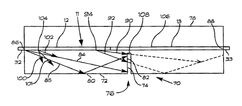
FIG. 3 is a side elevation view of a MIOC 70 according to the present
invention. The MIOC 70 is formed in a substrate 72 in the manner described
above and also has an optical waveguide network 11 that includes optical
waveguides 12-14 formed on a first surface 73 as described above and shown in
FIG. 1 A. The substrate 72 preferably has a thickness of about 1000 microns.
The
MIOC 70 has a single trench 74 formed in the central bottom portion 76 of the
substrate 72. The trench 74 preferably has a depth in the range of about 700
to
950 microns and a width of about 0.003 in. to 0.012 in. Therefore, the depth
of
CA 02328789 2004-05-21
-g-
the trench 74 is preferably about 70% to 95% of the thickness of the substrate
72.
The trench 74 may be filled with a light absorbing material 75 such as India
ink.
The MIOC 70 further includes a cover 78 mounted to a top surface 79 of
the substrate 72. The cover 78 also preferably formed of LiNb03. The cover 78
is
preferably a block having rectangular outer surfaces and a thickness of about
1000
microns, or the same thickness as the substrate 72. The cover 78 provides
additional structural integrity to prevent the MIOC 70 from breaking where the
trench 74 is formed. Other embodiments include the use of a 500 micron thick
cover 78.
The trench 74 in MIOC 70 blocks light rays having single and triple
reflections off the bottom surface 80 and top surface 106 and also blocks
light
from scatter sources within the MIOC 70 including the optical waveguides 12-
14.
In FIG. 3, the arrows formed of solid lines represent rays of stray light in
the
MIOC 70. The dashed arrows represent the paths that rays incident upon the
side
82 of the trench 74 would have followed if they were not blocked by the trench
74.
The arrows 84 and 85 represent light that is scattered into the MIOC 70 at
the input facet 86. The ray 84 follows a path in which it would reach the
output
facet 88 after a single reflection from the bottom surface 80 if the ray were
not
blocked by the trench 74. The arrow 85 represents a triple reflection path
that
would lead to the output facet 88 but for the blocking action of the trench
74.
The arrows 90 and 92 represent light rays that enter the MIOC 70 from a
scatter source 94 in the optical waveguide 12, 13, 14, or the Y-junction 20.
These
rays are blocked by the trench 74, but would not be blocked by the trenches in
the
prior art devices described above.
The arrows 100-102 represent still other light rays that enter the MIOC 70
from another scatter source 104. Only rays that pass over the inner end 108 of
the
trench 74 can reach the outputs of the MIOC 70.
FIGS. 4 and 5 show a comparison of the thicknesses of the typical prior art
trenched MIOC 10 and the MIOC 70 at the thinnest portions. Because of the
cover layer 78, the thickness t, of the MIOC 70 where the trench 74 is formed
is
about 1050 to 1300 microns. In contrast the thickness t2 of the prior art MIOC
10
CA 02328789 2004-05-21
-9-
is typically about 700-950 microns. The greater thickness of the MIOC 70 makes
it more mechanically stable than the prior art device.
FIG. 6A is a side elevation view of a MIOC 120 constructed according to
the principles of the present invention. As in FIG. 3, the MIOC 120 in FIG. 6A
includes a central trench 122 in the substrate 72 of the MIOC 120 under the
optical waveguides 12-14 as described above with reference to FIG. lA. As
shown in FIGS. 6A and 6B, the MIOC 120 also includes a groove 126 formed in a
side 128 of the MIOC 120. The side groove 126 extends across both the
substrate
72 and the side of the cover 78. The bottom trench 122 has a depth of about
700
to 950 microns. The side groove 126 extends into the substrate 72
approximately
50-500 microns, traversing the entire height of the MIOC 120.
FIG. ? is a top plan view illustrating a MIOC 140 according to the present
invention having a central bottom trench 142 and a plurality of grooves 143-
144
formed in a side surface 141. The trench 142 is similar to the trench 122
shown in
FIG. 6. The side grooves block rays that reflect from the sides of the MIOC
140.
For example, a ray 145 from the input fiber pigtail 32 will be blocked by the
side
groove 143. A ray 147 that misses the side groove 143 will be blocked by the
side
groove 144. A ray 149 will be blocked by the bevel 148. The MIOC 140 may
also include one or more bevels 148. The bevels 148 are formed by forming a
"V" shaped cross section groove in the surfaces of the MIOC 140. The side
bevels
or trenches and the bottom trenches may or may not be co-located in the same
plane. Different locations will require different widths and depths of the
side and
bottom trenches. The preferred locations for side . and bottom trenches are
dependant upon the IOC design length, width and thickness.
FIG. 8 is a top plan view of the substrate 72 on which the optical
waveguides 12-14 (not shown in FIG: 8) are formed. FIG. 8 shows an electrode
pattern 150 suitable for use with a MIOC constructed according to the present
invention. Electrode pads 152 and 154 extend to an edge 156 of the substrate.
FIG. 9 is a side view showing electrical contacts 158 and 160 arranged to
access
the electrode pattern 150 through the bond line 162 between the substrate 72
and
the cover 78.
CA 02328789 2004-05-21
-10-
Electrical accessibility of the device has been proven possible through the
cut side of the chip when diced after the full cover 78 has been attached.
This
gives the added benefit of preventing surface contamination of the integrated
optic
chip, and it prevents electrical discharges across its face when using
nonconductive epoxy at the interface as is currently done with the feet. This
method could be utilized on other integrated optical devices where
polarization
cross coupling, PNR, contamination, or strength of the device is an issue.
An important feature in the design of this invention is the extreme depth of
the trench. The trenches in the MIOC's according to the present invention are
approximately 700-950 microns in depth, which approaches the optical waveguide
structure. The total depth of the device without the cover is 1000 microns.
This _
deep trench design will block many more reflections than the typical 50-300
micron depth trenches currently in use. Without the foot being the entire
length of
the chip, this design would not be feasible, since the resultant chip would be
so
fragile that it should not stand up to the handling, temperature, mechanical
shock
or vibration requirements.
FIG. 10 graphically illustrates the effect of a 950 ~,m deep trench on the
extinction ratio of the MIOC 70 of FIG. 3. The upper graph represents the
baseline extinction ratio of a conventional MIOC that does not have a trench.
The
baseline extinction ratio is seen to be about -58 dB. Of the two lower lines,
the
dark line graph represents the extinction ratio of the MIOC 70' with the
trench 74
filled with India ink. The lighter line represents the extinction ratio of the
MIOC
70 with the trench 74 without any absorbing material added. The extinction
ratio
improves to about -74 dB for the 950 p,m deep trench.74 filled with India ink
and
to about -73 dB for the trench 74 alone.
FIG. 11 graphically illustrates the effect of increasing trench depth on the
extinction ratio. The baseline extinction ratio is about -57 dB for a single
trench
having a depth of 200 yam. The extinction ratio improves to about -58 dB when
the trench depth is increased to 700 ysm. Increasing the trench depth to 800
yam
resulted in another small improvement to about -59 dB. At a trench depth of
950
yam there is a dramatic improvement in the extinction ratio to about -76 dB.
CA 02328789 2000-12-19
FIG. 12 graphically illustrates the effect of single versus multiple trenches
having a depth of 7S0 pm. The chip initially had a polarization extinction
ratio of
-58 dB. Adding a single center trench of 750 microns in depth improved the
polarization extinction ratio to -74 dB. Two additional trenches degraded the
polarization extinction ratio to -62 dB.
The structures and methods disclosed herein illustrate the principles of the
present invention. The invention may be embodied in other specific forms
without departing from its spirit or essential characteristics. The described
embodiments are to be considered in all respects as exemplary and illustrative
rather than restrictive. Therefore, the appended claims rather than the
foregoing
description define the scope of the invention. All modifications to the
embodiments described herein that come within the meaning and range of
equivalence of the claims are embraced within the scope of the invention.