Note: Descriptions are shown in the official language in which they were submitted.
CA 02329211 2000-10-18
WO 99/54894 PCT/US99/08832
METALLIZED FILM CAPACITOR FOR USE 1N iMPLANTABLE
DEFIBRILLATOR
BACKGROUND OF THE INVENTION
Field of the Invention
The present invention relates generally to electrical energy storage
capacitors, and more particularly to energy storage capacitors suitable for
use
in an implantable cardiac defibrillator.
s Background Information
Implantable defibrillators are implanted in patients who are at risk of
suffering cardiac arrhythmias, such as ventricular fibrillation, that can
cause
sudden death. The defibrillator detects the occurrence of ventricular
fibrillation
and automatically delivers defibrillating therapy in the form of a high-energy
1o shock to the cardiac tissue. Implantable defibrillators in their most
general form
include appropriate electrical leads and electrodes for collecting electrical
signals
generated by the heart, and for delivering electric shocks to the heart. Also
included are batteries and energy storage capacitors, and control circuitry
connected to the leads, batteries and capacitors. The control circuitry senses
~ 5 the electrical activity of the heart and controls the charging of the
capacitors and
the delivery of the shocks through the leads to the heart.
Defibrillation therapy generally involves rapid delivery of a relatively large
amount of electrical energy to the heart at high voltage. Typical values
include
20 joules or more at 700 volts or more. Presently available batteries suitable
for
2o use in implantable defibrillators are not capable of delivering energy at
such
levels directly. Consequently, it is customary to provide a high-voltage
energy
storage capacitor that is charged by the battery via appropriate voltage
transformation and charging circuitry. To avoid wasting battery energy, the
high-voltage energy storage capacitor is not maintained in a charged state,
but
25 rather is charged after fibrillation has been identified by the control
circuitry and
immediately prior to delivering the shock.
The amount of electrical energy that must be transferred to cardiac tissue
to effect defibrillation is quite large by the standards of other implantable
cardiac
1
CA 02329211 2000-10-18
WO 99/54894 PCT/US99/08832
stimulators, such as pacemakers and cardioverters, which treat bradycardia
and tachycardia, respectively. Consequently, the physical volume of the energy
storage capacitors employed in implantable defibrillators is substantial.
Together
with the battery, the energy storage capacitor presents a major limitation to
s reducing the overall size of the implanted device.
Conventional energy storage capacitors used in implantable defibrillators
have employed an aluminum electrolytic capacitor technology that had been
developed for photoflash capacitors. Aluminum electrolytic capacitors have
plates of aluminum foil separated by a porous layer, often paper, impregnated
with a viscous liquid electrolyte comprising ethylene glycol plus additives.
Alternating layers of foil and paper are wound in a spiral about a mandrel to
form
a cylindrical capacitor. Electrical leads are attached to respective separate
foil
layers. The wound capacitor is placed in a cylindrical aluminum can, or
housing,
closed at one end and open at the other. The dielectric is formed at the
electrolyte-to-plate intertace by applying a controlled direct current between
the
leads of the capacitor. Periodically throughout life of the capacitor,
especially
after periods of non-use, that same process must be used to re-form the
dielectric of the aluminum electrolytic capacitor. To complete the
construction
of the aluminum electrolytic capacitor, the open end of the aluminum can is
20 . closed by an elastomeric seal, through which the electrical leads
project. The
elastomeric seal prevents Leakage of electrolyte from the aluminum can, but
does not provide an hermetic seal. This permits venting of hydrogen gas that
is
normally liberated in the aluminum electrolytic capacitor during use.
While aluminum electrolytic capacitors have been used successfully in
25 implantable defibrillators, certain of their characteristics are regarded
as
disadvantageous. For example, the outgassing characteristic is undesirable in
a capacitor that is contained within an implantable device that itself must be
hermetically sealed against intrusion by body fluids. The device either must
be
provided with internal hydrogen adsorbers or else made permeable to hydrogen
3o to prevent an internal buildup of pressure. The relative thickness of the
aluminum foil plates and paper separators, as well as the head room required
at the ends of the capacitor housing, place upper limits on the energy density
of
2
CA 02329211 2000-10-18
WO 99/54894 PCT/US99/08832
the aluminum electrolytic capacitor, resulting in a relatively bulky device.
This
is undesirable in the context of pectorally implanted defibrillators which,
for
reasons related to ease of implantation, comfort and cosmetics, are desired to
be as small as possible. Typical aluminum electrolytic photoflash capacitors
s have energy densities of about 1.8 Joules per cubic centimeter. Also,
aluminum
electrolytic capacitors typically have a maximum working voltage of about 380
V, whereas implantabie defibrillators are usually designed to deliver a shock
at
700 V or more. Consequently, two capacitors must be employed in series to
achieve the desired working voltage. This results in inefficient space
utilization
o in the implantable device. The need to periodically reform the dielectric of
the
aluminum electrolytic capacitor is also an undesirable characteristic of a
capacitor enclosed in a self contained, battery powered, implanted device. The
periodic reformation consumes energy from the battery that otherwise would be
available for therapeutic use, thereby reducing the longevity of the implanted
device.
Another capacitor technology that has been considered for use in
impiantable defibrillators is the ceramic dielectric capacitor. The ceramic
capacitor has advantages over the aluminum electrolytic capacitor in that it
is
free of outgassing and does not need periodic reformation. Nevertheless, the
20 , ceramic capacitor has been difficult to manufacture with the working
voltage and
reliability characteristics needed for use in an implantable defibrillator.
For
example, working voltages above about 400 V have been difficult to achieve.
A single local defect in the ceramic dielectric can result in a short circuit
between
the plates, resulting in catastrophic failure of the capacitor. Also, ceramic
2s capacitors are relatively heavy. Excess weight is undesirable in an
implantable
device because it can complicate the task of reliably anchoring the device to
adjacent tissue and may raise issues of patient comfort.
Yet another capacitor technology that has been considered for use in
implantable defibrillators is the thin polymer film capacitor. Such capacitors
3o employ a thin polymer dielectric film between the metallic capacitor
plates, as
opposed to the electrolyte dielectric material of the typically employed
photoflash
aluminum electrolytic capacitor. The plates of the thin polymer film capacitor
3
CA 02329211 2000-10-18
WO 99/54894 PC1'/US99/08832
usually take the form of very thin metal layers that are vapor deposited
directly
to the dielectric substrate to a thickness of about 150 to 350 angstroms. The
result is a so-called metallized polymer film that provides both the
dielectric and
plate functions of the capacitor. Typically, two layers of metallized polymer
film
are overlaid and are tightly wound about a mandrel to form a wound cylindrical
capacitor. The metaliized layers on the two polymer films are offset from
opposite respective edges of the films, allowing alternate plates of the
spiral-wound structure to be soldered together~at opposite ends of the
cylindrical
capacitor and connected to respective leads. A capacitor wound from metallized
o polymer film can be constructed with a relatively high energy density
because
of the efficient use of space permitted by the extremely thin metal plates,
and
because working voltages well in excess of 700 V can be achieved in a single
capacitor. The energy density that can be achieved is limited primarily by the
manufacturability of polymer films of arbitrarily small thickness, and by the
dielectric properties of the particular polymer film, which dictate the
minimum
thickness required for a particular design voltage. Energy densities of about
one
(1) Joule per cubic centimeter are typical for polyester film capacitors, for
example. Polyester has a dielectric constant of about 2.5 to 3Ø
An advantageous characteristic of the metallized, thin polymer film
2o capacitor is its ability to self-heal, or clear, minor defects in the
dielectric when
subjected to an initial clearing voltage greater than its designed working
voltage.
This characteristic provides a capacitor of high reliability. Dining clearing,
imbedded foreign particles or micro-flaws in the capacitor dielectric lead to
localized breakdowns of the film dielectric. The breakdown event results in an
arc between the two metalfized layers that develops a localized high
temperature
and pressure. A puncture develops in the polymer film, and the thin metallized
plate in the vicinity of the failure site is rapidly vaporized and blown away
from
the puncture. The evaporation of the electrode around the arc causes it to
extinguish, which electrically isolates the two plates on either side of the
3o dielectric film in the vicinity of the puncture. This prevents large-scale
damage
and catastrophic failure of the capacitor. The clearing process removes an
electrode area that is a very small percentage of the entire area of the
capacitor
4
CA 02329211 2000-10-18
WO 99/54894 PCT/US99/08832
plate electrodes, resulting in no significant loss of capacitance. As a
general
rule, the more flexible and elastic the film material is, and the lower the
pressure
between the winding layers, the greater the probability that a puncture will
self heal. When inter-layer (radial) pressures are high, the gas pressure
associated with the arc increases rapidly, damaging adjacent layers and
extinguishing the arc prematurely. This incomplete burning leaves behind a
carbon residue that continues to conduct, leading to a thermal runaway that
melts many layers of metallized plastic film arid generates a catastrophic,
high
resistance short.
~o Some polymer films demonstrate better clearing characteristics than
others do. In general, polymers that burn well, i.e., that will sustain a
flame once
ignited, have good clearing properties. Such polymers usually have oxygen in
their molecular structure, e.g., polyester, but there are notable exceptions,
such
as polypropylene.
~5 One promising polymer film for constructing a high energy-density thin
film capacitors is polyvinylidene fluoride, or PVDF. This material has a very-
high
dielectric constant, i.e., k=12, which presents the possibility of
constructing a
capacitor with very thin films. This would permit more windings within a given
capacitor diameter, which increases the plate area within a given cylindrical
2o volume and increases the energy density. Energy densities of about 4 Joules
per cubic centimeter are possible with a PVDF dielectric. Also, PVDF exhibits
lower leakage than aluminum electrolytic capacitors, with leakage currents on
the order of tens of micro-amps rather than hundreds or thousands of micro-
amps. Compared with polyester, however, PVDF has relatively poor self-
25 healing, or clearing, characteristics.
Evaluations of capacitors constructed using metallized thin films of PVDF
have shown electrical degradation at voltages lower than expected, considering
the inherent voltage breakdown characteristics of PVDF. For example, two
metallized layers of PVDF were cylindrically (spirally) wound on a mandrel
3o having a diameter of about 2 to 3 mm. The layers were wound until the
capacitor had a diameter of about 14.5 to 15 mm, with a height of about 50 mm.
The PVDF film had a thickness of about 6 microns, and the metallized layers
5
CA 02329211 2000-10-18
WO 99/54894 PCT/US99/08832
were offset about 2.5 mm from respective opposite ends of the cylindrical
construct. In theory, such a capacitor should have withstood at least 2000 V
without breakdown, but in fact exhibited voltage breakdown at about 800 V to
about 1050 V. Subsequent examination of the failed capacitors revealed many
successful clearings of minor defects, as welt as some catastrophic failures
involving localized voltage breakdown through several layers of dielectric
film.
The catastrophic failures had not taken place at locations distributed
uniformly
over the film, but rather had been concentrated at the beginning (near the
mandrel) and at the end (on the surface of the capacitor) of the film. It was
~ o noted that the failures at the end of the windings were due to shorting
between
the edges of the two films. The polymer flm from which the capacitor had been
wound had not been de-metallized at the Last few turns. It was also noted that
the film windings at the center of the capacitor, i.e., at the beginning of
the
winding near the mandrel, were very wrinkled. The wrinkling is believed to
have
~ 5 been caused by the winding process in which the first few turns resist
bending
smoothly at the small radius involved. The wrinkling may have resulted in
localized areas of high inter-layer pressure in which breakdown events that
ordinarily would have terminated in a self healing, nevertheless cascaded
through several layers into catastrophic failure.
2o It would be desirable to provide improvements in the design of and
manufacturing steps for making thin film capacitors to permit the full
potential of
very thin films of PVDF to be exploited to increase the energy density of the
capacitor. These and other advantages are provided by the present invention.
25 SUMMARY OF THE INVENTION
In accordance with one aspect of the present invention, a thin film
capacitor for use in an implantable defibrillator includes first and second
dielectric polymer film layers, each of the first and second dielectric
polymer film
layers having a metallized film on ane side thereof. The first and second
3o dielectric polymer film layers are overlain on each other and wound
spirally with
the metatlized film of one layer adjacent the dielectric polymer of the other
layer.
6
CA 02329211 2000-10-18
WO 99/54894 PCT/US99/08832
The beginnings of the metallized films are offset from the respective
beginnings
of the first and second polymer film layers in the direction of winding.
In accordance with a further aspect of the present invention, the first and
second dielectric polymer film layers are tapered in increasing thickness from
a
middle portion of uniform thickness toward the respective beginnings and ends
of the dielectric polymer film layers.
In accordance with yet another aspect of the present invention, each of
the first and second dielectric polymer film layers comprises at least two
layers
of differing polymer materials, one of which provides the primary dielectric
~o characteristics of the capacitor and the other of which provides enhanced
self-
healing characteristics.
1t is an object of the present invention to provide an improved electrical
energy storage capacitor for use in an implantable defibrillator.
Other objects and advantages of the invention will be apparent from the
following descriptions of preferred embodiments made with reference to the
drawings.
BRIEF DESCRIPTION OF THE DRAWINGS
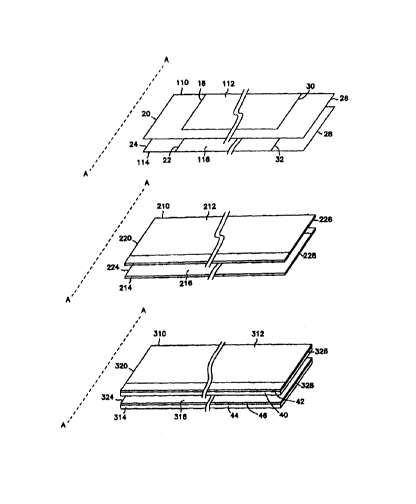
Fig. 1 is an end view of a prior art arrangement of metallized polymer
2o films prior to being wound spirally about a mandrel to form a cylindrical
capacitor.
Fig. 2. is a perspective view of the prior art arrangement of metaliized
polymer films of Fig. 1.
Fig. 3 is a perspective view of a first embodiment of an arrangement of
metallized polymer films in accordance with the present invention, prior to
being
25 wound spirally about a mandrel to form a cylindrical capacitor.
Fig. 4 is a perspective view of a second embodiment of an arrangement
of metallized polymer films in accordance with the present invention, prior to
being wound spirally about a mandrel to form a cylindrical capacitor.
Fig. 5 is a perspective view of a third embodiment of an arrangement of
3o metaNized polymer films in accordance with the present invention, prior to
being
wound spirally about a mandrel to form a cylindrical capacitor.
7
CA 02329211 2000-10-18
WO 99/54894 PCT/US99/0883Z
DETAILED DESCRIPTION OF THE PREFERRED EMBODIMENTS
Referring to Figs. 1 and 2, a prior art arrangement of two layers of
metallized polymer dielectric film is shown, prior to being wound spirally on
a
mandrel about axis A to form a cylindrical capacitor. The thickness of the
layers,
as illustrated, is greatly exaggerated. Polymer film layer 10 has deposited on
the
upper side thereof a thin metallic layer 12. Along one edge of film layer 10,
perpendicular to the winding axis A, metallic layer 12 is spaced therefrom by
a
margin M. Similarly, polymer film layer 14 has deposited on the upper side
thereof a thin metallic layer 16. Along one edge of film layer 14,
perpendicular
~o to the winding axis A and opposite to the edge referred to above with
regard to
polymer film layer 10, metallic layer 16 is spaced therefrom by a margin "M".
Polymer layers 10 and 14 are offset relative to each other in the direction of
the
winding axis A by an offset "O", such that the edge having the margin "M" of
each polymer layer is recessed relative to the non-margined edge of the other
~5 polymer layer. When layers 10 and 14, with their respective metallic layers
12
and 16, are wound spirally about winding axis A, one edge of metallic layer 12
is exposed at one end of the resulting cylindrical capacitor, whereas the
opposite
edge of metallic layer 16 is exposed at the opposite end of the resulting
cylindrical capacitor. Solder is sprayed on one end of the capacitor in
electrical
2o contact with a continuous edge of one, but only one, of the metallic
layers.
Similarly, solder is sprayed on the opposite end of the capacitor in
electrical
contact with a continuous edge of only the other metallic layer.
Referring to Fig. 3, a first embodiment of the present invention is
illustrated in which two metallized layers of polymer dielectric film are
shown
25 prior to being wound spirally about a mandrel to form a cylindrical
capacitor.
Components that correspond to similar components described above with
respect to the prior art construction illustrated in Figs. 1 and 2 are
designated by
similar reference numerals in the one hundred series. Film layer 110 has a
metaliized layer 112 that begins at a location 18 offset in the direction of
winding
3o from the starting end 20 of layer 110. Likewise, film layer 114 has a
metallized
layer 116 that begins at a location 22 offset in the direction of winding from
the
starting end 24 of layer 114. The amount of offset of the beginnings 18 and 22
8
CA 02329211 2000-10-18
WO 99/54894 PCTNS99/08832
of metallized layers 112 and 116 from the beginnings 20 and 24 of film layers
112 and 114 should be at least several multiples of the circumference of the
mandrel on which the capacitor is to be wound. This will assure that wrinkling
at the start of the winding process will be confined to an area of the
windings
devoid of metallization, thereby avoiding injury to the dielectric layer that
lies
between the metallized plates. A similar offset is provided at the ends 26 and
28 of film layers 110 and 114, respectively, whereby the metallized layers 112
and 116 terminate at locations 30 and 32. The amount of offset of the
metallized
layers at the end of the winding should be at least several multiples of the
o circumference of the capacitor at the end of winding. This will prevent
failures
due to shorting at the end of the windings.
Referring to Fig. 4, a second embodiment of the present invention is
illustrated in which two metallized layers of polymer dielectric film are
shown
prior to being wound spirally about a mandrel to form a cylindrical capacitor.
~5 Components that correspond to similar components described above with
respect to the prior art construction illustrated in Figs. 1 and 2, and the
first
embodiment illustrated in Fig. 3, are designated by similar reference numerals
in the two hundred series. Film layer 210 has a metallized layer 212.
Likewise,
film layer 214 has a metallized layer 216. Each of film layers 210 and 214 is
of
2o uniform thickness in a middle portion, but is tapered to an increased
thickness
at the beginning ends 220 and 224 and at the terminating ends 226 and 228.
As preferred, the film layer is tapered to an increased thickness over a
distance
in the direction of winding that is at least several multiples of the
circumference
of the mandrel, at the starting end, and at least several multiples of the
capacitor
25 circumference at the terminating end. By increasing the thickness of the
dielectric at the ends of the winding, where failure modes are more likely to
occur, the reliability of the capacitor is increased.
Referring to Fig. 5, a third embodiment of the present invention is
illustrated, in which two metallized layers of polymer dielectric film are
shown
3o prior to being wound spirally about a mandrel to form a cylindrical
capacitor.
Components that correspond to similar components described above with
respect to the prior art construction illustrated in Figs. 1 and 2, and the
first
9
CA 02329211 2000-10-18
WO 99/54894 PCT/US99/08832
embodiment illustrated in Fig. 3, are designated by similar reference numerals
in the three hundred series. Film layer 310 has a metallized Layer 312.
Likewise, film layer 314 has a metallized layer 316. Unlike previously
described
embodiments, polymer film layer 310 is itself comprised of two layers of
different
polymers, the primary layer 40 being polyvinylidene fluoride, and the
secondary
layer 42 being polyester. The metallized layer 312 is deposited on the
secondary layer 42. As preferred, the PVDF layer 40 with its high dielectric
constant primarily determines the energy density characteristics of the
capacitor.
The polyester layer 42, with its significantly lower dielectric constant, is
preferred
o to be much thinner than the PVDF layer 40 so as not to adversely affect the
volume of the capacitor. The polyester layer 42 serves to improve the
clearing,
or self healing characteristics of the composite dielectric layer 310.
Similarly,
polymer film layer 314 is itself also comprised of two layers of different
polymers,
the primary layer 44 being polyvinylidene fluoride, and the secondary layer 46
~5 being polyester. The metallized layer 316 is deposited on the secondary
layer
46.
Three specific embodiments have been described and illustrated in Figs.
3, 4 and 5. It should be understood, however, that combining the features
illustrated in the first three embodiments can make other embodiments. For
2o example, the offsets of the metallic layers at the starting and terminating
ends
. of the polymer film layers, as shown in Fig. 3, can be combined with the
tapered
dielectric as shown in Fig. 4, or with the composite dielectric as shown in
Fig. 5,
or with both the tapered dielectric of Fig. 4 and the composite dielectric of
Fig.
5. Another desirable combination is the tapered dielectric of Fig. 4 in
25 combination with the composite dielectric of Fig. 5. In the embodiment
illustrated
in Fig. 5, the preferred materials for the dielectric layer is PVDF and the
preferred
material for the self healing enhancing layer is polyester. Other polymers
could
be substituted. The self healing enhancing layer could be any polymer material
having better self healing characteristics than the material of the dielectric
layer,
3o although polymers having oxygen in their molecular structure are preferred.