Note: Descriptions are shown in the official language in which they were submitted.
CA 02329416 2000-10-18
WO 99/56358 PCT/US99/07197
-1-
NARROW SPECTRAL 'WIDTH HIGH POWER DISTRIBUTED
FEEDBACK SEMICONDUCTOR LASERS
FIELD OF THE INVENTION
This invention pertains generally to the field of semiconductor diode
lasers and particularly to edge emitting distributed feedback semiconductor
lasers.
BACKGROUND OF 1'HE INVENTION
Semiconductor diode lasers are formed of multiple layers of
semiconductor materials. The typical semiconductor diode laser includes an n-
type
layer, a p-type layer and an undoped active layer between them such that when
the
diode is forward biased electrons and holes recombine in the active region
layer
with the resulting emission of light. The layers adjacent to the active layer
typically
have a lower index of refraction than the active layer and form cladding
layers that
confine the emitted light to the active layer and sometimes to adjacent
layers.
Semiconductor lasers may be constructed to be either edge emitting or surface
emitting. In an edge emitting Fabry-Perot type semiconductor laser, crystal
facet
mirrors are located at opposite edges of the multi-layer structure to provide
reflection of the emitted light back and forth in a longitudinal direction,
generally in
the plane of the layers, to provide lasing action and emission of laser light
from one
of the facets. Another type of device, which may be designed to be either edge
emitting or surface emitting, utilizes distributed feedback structures rather
then
conventional facets or mirrors, providing feedback for lasing as a result of
backward
Bragg scattering from periodic variations of the refractive index or the gain
or both
of the semiconductor laser structure.
Semiconductor lasers having CW power in the watt-range and narrow
bandwidth, e.g., less than 2 A full width half maximum (FWHM), would be
desirable for a variety of applications. Examples include 0.894 win diode
lasers
CA 02329416 2000-10-18
WO 99/56358 PCT/US99/07197
-2-
which may be used for polarizing Cs to generate spin-polarized Xe gas for
magnetic
resonance imaging, low-chirp pump sources for solid state lasers, and in
spectroscopy sources for monitoring environmental gases. Conventional broad
stripe (>_ 25 pin) semiconductor lasers used for obtaining high powers
typically have
a spectral width of about 20 A FWHM or more at high drive levels and broaden
further under quasi-CW operation. Significant improvements in spectral width
can
be obtained using distributed feedback (DFB) gratings or distributed Bragg
reflectors (DBR) rather than Fabry-Perot mirror facets for optical feedback.
278
mW CW power with about 1 A of wavelength variation, resulting from mode
hopping, has been reported for narrow-stripe DBR lasers. J.S. Major, et al.,
Electron. Lett. Vol. 29, No. 24, p. 2121, 1993. Using DFB phase-locked laser
arrays, narrow bandwidth operation has been obtained from large apertures at
relatively long wavelengths (~,=1.3 p,m to 1.5 pin). 120 mW pulsed operation
has
been reported from a 45 ~m aperture device (~,=1.3 pin), Y. Twu, et al.,
Electron.
i5 Lett. Vol. 24, No. 12, p. 1144, 1988, and 85 mW CW from a 72 p.m aperture
device (~,=1.55 p,m), K.Y. Liou, et al., Tech. Dig. 13th IEEE Int. Semicond.
Laser
Conf., Paper D7, 1992. For applications where (lateral) spatial coherence is
not
necessary, a broad-stripe laser with a DFB grating is apparently well suited
for
achieving high CW powers with narrow spectral line width.
A limitation is encountered with DFB lasers designed to operate at
shorter wavelengths including visible light wavelengths, in that conventional
diode
lasers grown on GaAs substrates, which can emit in the range of wavelengths
between about 0.6 pin to 1.1 p,m, generally have optical confinement layers
containing aluminum as well as cladding layers containing aluminum. Due to the
high reactivity of aluminum (i.e., essentially instant oxidation when exposed
to air),
it has proven to be very difficult to make single frequency lasers of the DFB
type in
the foregoing wavelength range in which the grating is buried within the mufti-
layer
semiconductor structure. Consequently, the commercially available high power,
narrow line width lasers have been of the distributed Bragg reflector (DBR)
type, in
which the grating is outside of the active losing part of the structure.
However,
CA 02329416 2000-10-18
WO 99/56358 PCT/US99/07197
-3-
such DBR devices suffer from the major drawback of mode hopping that occurs
with increasing drive current due to changes in the lasing-region index of
refraction
with increasing drive power.
SUMMARY OF THE INVENTION
The present invention encompasses a high power edge emitting
semiconductor laser with very narrow spectral width that can be tailored to
operate
at precisely selected wavelengths including wavelengths in the visible range.
In
accordance with the invention, typical CW powers in the watt range are
obtainable
with a narrow line width of 2 A FWHM or less. Consequently, such lasers are
well
suited to applications requiring precise narrow line width laser sources, such
as for
polarizing cesium or rubidium for use in magnetic resonance imaging with spin
polarized xenon.
The edge emitting semiconductor laser of the invention includes a
substrate and an epitaxial structure preferably grown on orientation on the
substrate.
The epitaxial structure includes a layer with an active region at which light
emission
occurs, upper and lower confinement layers adjacent the active region layer,
upper
and lower cladding layers adjacent the confinement layers, outer edge faces
perpendicular to the active region layer, and electrodes by which voltage can
be
applied across the epitaxial structure and the substrate. A distributed
feedback
grating is formed on an aluminum free section of the upper confinement layer.
The
grating is comprised of periodically alternating elements differing from one
another
in dielectric constant, and thus generally in index of refraction, to provide
optical
feedback for a selected effective wavelength of light generation from the
active
region. Because the distributed feedback grating in accordance with the
invention is
formed in a layer above the active region, regrowth problems and the
propagation of
dislocations that are encountered with gratings formed below the active region
layer
are avoided. In addition, it has been found, in accordance with the invention,
that
by utilizing a confinement layer at least a section of which is aluminum free,
the
grating may be readily etched in the aluminum free confinement layer to
provide a
grating surface on which additional epitaxial layers may be grown without
difficulty.
CA 02329416 2000-10-18
WO 99156358 PCT/US99/07197
Such devices are well-suited to being formed to provide a wide emitting
aperture,
preferably at least 25 pin to provide high power lasing, which may be defined
by
current confinement.
The invention may be incorporated in semiconductor lasers having a
GaAs substrate and epitaxial layers (preferably grown on (100) orientation on
the
substrate) including an active region layer with single or multiple quantum
wells of
InGaAs surrounded by InGaAsP barrier layers, optical confinement layers of
InGaP,
with the distributed feedback grating formed in the top surface of the upper
InGaP
confinement layer, and cladding layers of InGaAIP or AIGaAs. The thickness of
the
upper confinement layer and the spacing of the grating from the active region
layer
is preferably at least about 0.2 p,m to ensure small coupling to the grating.
Small
grating coupling coefficient, x, is needed to maintain a xL product of about
unity,
where L is the cavity length between the edge faces of the laser, which, in
turn,
ensures both efficient DFB laser operation as well as single-longitudinal-mode
operation to high drive levels above threshold. Since watt-range lasers
require long
cavities (L >_ 1 mm), to keep xL ' 1 it is of critical importance to have a
low x
value. Such structures can be formed to operate in the range of 1 watt CW with
a
line width of less than 1 A and at 1 watt pulsed (Sp,s-wide pulses) with a
line width
of 1.2 A. Because the upper confinement layer of InGaP is aluminum free, it
may
be etched in a conventional manner to leave a surface of the grating on which
regrowth is readily accomplished.
Further objects, features and advantages of the invention will be
apparent from the following detailed description when taken in conjunction
with the
accompanying drawings.
BRIEF DESCRIPTION OF THE DRAWINGS
In the drawings:
Fig. 1 is a schematic diagram illustrating an example of a
composition for the active region layer and adjacent confinement and cladding
layers
in accordance with the invention.
CA 02329416 2000-10-18
WO 99/56358 PC'T/US99/07197
-5-
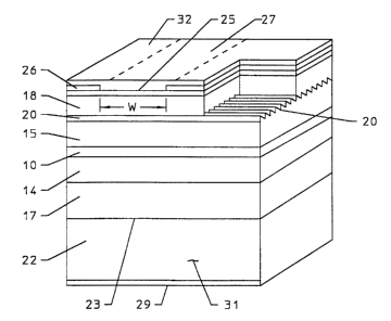
Fig. 2 is a perspective view of an exemplary semiconductor laser
formed in accordance with the invention.
Fig. 3 are plots of CW power and wallplug efficiency as a function of
drive current for the exemplary device of Fig. 2.
Fig. 4 is a plot of CW emission wavelengths for the exemplary device
of Fig. 2.
Fig. 5 are plots of emission wavelengths for pulsed operation (quasi-
CW) of the exemplary device of Fig. 2.
Fig. 6 is a simplified view of the detailed mufti-layer structure of an
exemplary device in accordance with the invention.
Fig. 7 is an illustrative diagram of an alternative exemplary
composition for a semiconductor laser in accordance with the invention.
Fig. 8 is an illustrative diagram of an alternative composition for a
semiconductor laser which has an asymmetric transverse optical waveguide.
DETAILED DESCRIPTION OF THE INVENTION
For purposes of illustrating the present invention, a diagram
illustrating an exemplary mufti-layer waveguide structure in accordance with
the
invention is shown in Fig. 1 along with a diagram of the band gap energy for
the
several layers. The exemplary structure of Fig. 1 includes an active region
layer 10
including double quantum wells 11 of InGaAs surrounded by InGaAsP barrier
layers 12, a lower confinement layer 14 and an upper confinement layer 15,
both
formed of InGaP, and a lower cladding layer 17 of n-type InGaAIP and an upper
cladding layer 18 of p-type InGaAIP adjacent to the lower and upper
confinement
layers, respectively. A distributed feedback grating 20 is formed at the top
of the
upper confinement layer 15. The upper confinement layer is formed of InGaP and
is free of aluminum. Thus, once the grating 20 has been formed in the upper
confinement layer 15, the upper cladding layer 18 and subsequent layers may be
readily grown over the grating. The right-hand side of Fig. 1 is a diagram
illustrating the band gap energy levels of these various layers.
CA 02329416 2000-10-18
WO 99/56358 PCT/US99/07197
A simplified perspective view of a semiconductor laser incorporating
the waveguide layers of Fig. 1 is shown in Fig. 2. The layers illustrated in
Fig. 2
are epitaxially grown on a GaAs substrate 22. It is preferred that the top
surface 23
of the substrate 22 be the (100) surface and that the epitaxial layers be
grown on this
surface exactly on orientation. For exemplification only, current confinement
may
be provided to define the emitting aperture by insulating layers 26 of Si02
over a
cap layer 25 of p+ GaAs, with a top metal electrode 27 in contact with the cap
layer 25 at the top face of the laser between the insulating Si02 layers to
provide
electrical conduction thereto. A bottom metal electrode 29 is formed on the
bottom
face of the substrate 22 so that voltage may be applied across the
semiconductor
laser between the electrodes 27 and 29. The width W of the metal electrode 27
in
contact with the cap Iayer 25 defines the effective stripe width of the
semiconductor
diode in the active layer 10 at which light emission will occur.
A specific example of such a structure is a 100 p,m wide stripe laser
which operates at 1.1 W CW with a line width of 0.9 A, and at 1 W quasi-CW (5
ps
pulse width at 2 kHz repetition rate) with a line width of 1.2 A. The double
quantum well layers 11 are formed of Ino,~Gao.~,As between and separated by
InGaAsP (bandgap energy = 1.62 eV) barrier layers 12, with the optical
confinement layers 14 and 15 formed of Ino.4,Gao.s3P, and with the cladding
layers
17 and 18 formed of Ino.s (Gao.sAlo.s)o.sP~ The large bandgap of the Ino.s
(Gao.sAlO.s)o.sP cladding layers I7 and 18 ensures good carrier confinement
for these
structures, resulting in higher internal efficiencies than would be obtained
from an
entirely aluminum free structure. The grating 20 is a second-order grating
that is
holographically patterned and wet etched directly into the InGaP upper
confinement
layer 15 over the active region. As an example, the grating, which may have a
sinusoidal form, can have a period between adjacent peaks of the periodic
elements
of about 2740 A and a peak-to-peak depth of about 500 A. Because InGaP is less
prone to oxidation than aluminum containing compounds, regrowth over the
grating
is readily accomplished. Thus, the InGaAiP upper cladding layer 18 is simply
grown over the grating 20, followed by the p+ GaAs cap layer 25. This
structure
CA 02329416 2000-10-18
WO 99/56358 PCT/US99/07197
can be designed, for example, to lase at 0.894 pm. Multiple oxide stripe broad
area
laser structures may be processed from this material by cleaving the bars
perpendicularly to the stripe along the crystal facets to provide an emitting
edge face
31 and an opposite reflecting edge face 32 to produce 1 mm-long lasers with,
e.g.,
5 % reflectivity at the emitting edge face 3 l and 95 % facet reflectivity at
the
reflecting edge face 32.
The CW power-current curve 35 for a 1 mm-long, 100 ~m-wide laser
in accordance with the invention at 10° C as shown in Fig. 3, and
illustrates that the
threshold current density, J~" is 240 A/cm2, the differential quantum
efficiency, rid,
is 51 % , and the wallplug efficiency curve 36 shown in Fig. 3 illustrates
that the
wallplug efficiency rlP reaches a maximum value of 32 % at 1.1 W (7.3 times
threshold). By comparison, devices made without the distributed feedback
grating
but with otherwise the same structure and dimensions have, at 20° C, a
J,~ of 225
A/cm2 and rld of 62% with characteristic temperatures To=200K and T~=480K.
15 As illustrated in Fig. 4, the spectrum of the broad-area DFB laser of
the invention appears to be single frequency near threshold with a temperature
dependence of 0.6 t~/C and maintains a narrow line width at 1 W output power
as
shown by the right-hand peak in Fig. 4. The FWHM for the CW spectrum at 0.53
W is 0.5 A FWHM. At 1.1 W, if a width is approximated based on the envelope of
20 the peaks, the spectrum broadens to about 0.9 t~ FWHM. Under quasi-CW
conditions, as illustrated in Fig. 5, the spectrum is broader than the CW
spectrum,
which can be attributed to thermal-induced and carrier-induced transients
(chirp).
The spectra measured for 5 ~,s pulses at a frequency of 2 kHz yields widths of
0.9 A
and I.2 t;r FWHM at 0.5 W and 1.0 W, respectively, as shown by the lower and
upper spectra diagrams in Fig. 5. In contrast, the spectra near threshold of
Fabry-
Perot lasers have a width of over 10 A FWHM and reach 20 A FWHM at 1 W CW.
The angular FWHM of a lateral farfields for the broad area DFB lasers of the
invention is approximately 4° near threshold, 5° at 0.5 W, and
6.5° at 1.0 W under
both CW and pulse conditions, indicating that some spatial mode discrimination
CA 02329416 2000-10-18
WO 99/56358 PG"f/US99/07197
_g_
occurs as compared to the Fabry-Perot devices which have 8° FWHM
farfields at
low drive levels.
An exemplary detailed fabrication process for the large aperture DFB
lasers of the invention is given below, and forms the epitaxial layer
structure on a
GaAs substrate as illustrated in Fig. 6.
The grating base structure is grown in a low-pressure (50 mbar)
metal organic chemical vapor deposition (MOCVD) reactor at 700° C. The
substrate 22 is an epi-ready n+ GaAs substrate on orientation, (100). As
illustrated
in Fig. 6, the following epitaxial layers (with exemplary thicknesses shown)
are
grown in sequence on the substrate (including suitable buffer and transitional
layers
in addition to the main functional layers shown in Fig. 2): n-GaAs buffer
layer 40;
n-InGaP transition layer 41 (lattice matched); n-Ino.s(Gao_sAlo.s)o.sP lower
cladding
layer 17 (lattice matched) InGaP optical confinement layer 14 (lattice
matched);
InGaP slow growth rate layer 43 (lattice matched); InGaAsP transition barrier
layer
12 (lattice matched - Eg=1.62 eV); InGaAs quantum well 11; InGaAsP barrier
layer
12 (lattice matched - Eg=1.62 eV); InGaAs quantum well 11; InGaAsP transition
barrier layer 12 (lattice matched - Eg= 1.62 eV); InGaP slow growth rate layer
44
(lattice matched); InGaP optical confinement layer 15 (lattice matched). All n-
type
layers are Si doped.
The gratings are holographically defined in photoresist and then
transferred into the exposed InGaP confinement layer 15 using wet chemical
etching. The surface of the layer 15 is cleaned in a HF:DI water (1:10)
solution for
seconds. It is then rinsed in a DI (deionized) water solution for S minutes
and
blown dry with nitrogen gas. A solution of Shipley 1805 photoresist:Shipley
Type
25 P thinner (1:2) is spin coated onto the sample at 5000 rpm for 30 seconds.
The
coated sample is then baked in an oven at 90° C for 30 minutes.
The photoresist is exposed by light from an Ar-Ion laser. The light
travels through a 50%l50% beam sputter. Each leg of the split beam goes
through a
spatial filter to generate diverging coherent spherical waves. The light from
each of
30 the two beams is then reflected onto the sample. The sample is aligned such
that the
CA 02329416 2000-10-18
WO 99/56358 PCT/US99/07197
-9-
periodic lines produced by the laser are parallel to the crystal plane that
forms the
cleaved facet of the laser. The laser is set to 200 mW, with the power density
of
each leg measured at roughly 30 mW/sq. cm at the sample. The sample is exposed
under these condition for a time of 60 sec.
The exposed photoresist is then spray developed using Shipley ME-
321 developer on a spinner rotating at 2000 rpm for a time of 10 sec. The
sample is
then spray rinsed with DI water at 2000 rpm for 1 minute, and allowed to spin
dry
at 2000 rpm for 1 minute. The InGaP is etched in a solution of [Br2:HBr
(1:17)]:DI
(1:80) for 20 seconds and rinsed in DI water for 10 minutes. The sample is
then
blown dry with nitrogen gas. The sample is stripped in Shipley 1165
photoresist
stripper for 5 min and rinsed in DI water for 10 minutes. The surface is then
cleaned in acetone for 1 minute and methanol for 1 minute. This is followed by
rinsing in DI water for 3 minutes and blowing the sample dry with nitrogen
gas.
The surface is treated with a mild oxygen plasma etch in a Plasmatherm etcher.
25
sccm of 02 gas flows into the reactor maintained at a pressure of 2OmT. A 100W
plasma is excited for 4 minutes. The sample is etched in a buffered oxide etch
(BOE) - NF3:HF (20:1) for 30 seconds, and rinsed in DI water for 5 minutes.
The
sample is then blown dry with nitrogen gas.
The upper cladding layer and a highly doped cap are then grown over
the grating using the same MOCVD system. The In compounds are grown at
700° C
and are Zn-doped. The first GaAs layer is grown at 625° C and is Zn-
doped. The
last layer is grown at 575C and is C-doped. The following layers are grown in
sequence: p-Ino.s(AIo,SGao.s)o.sP uPPer cladding layer 18 (lattice matched); p-
InGaP
transition layer 46 (lattice matched); p-GaAs layer 47; p+-GaAs highly doped
cap
25 (p" 10~° ctri 3).
The following process is used to produce a broad-stripe current
confined laser using oxide isolation. Of course, current confinement may be
provided in a conventional manner via back-biased p-n junctions, proton
implantation, etc. , and lateral index guiding may also be utilized if
desired. Shipley
1805 photoresist is spin coated onto the sample at 5000 rpm for 30 seconds.
The
CA 02329416 2000-10-18
WO 99/56358 PCT/US99/07197
-10-
coated sample is baked in an oven at 90° C for 30 min. The photoresist
is exposed
in a Karl-Suss mask aligner with a first mask. The sample is aligned such that
the
stripes of the mask are perpendicular to the crystal plane that forms the
cleaved facet
of the laser. The exposed photoresist is developed in Shipley MF-321 with mild
agitation for 1 minute. The sample is then rinsed with DI water for 3 minutes,
and
blown dry with nitrogen gas. The developed sample is baked in an oven at
110° C
for 30 min. The GaAs cap 25 is etched in a NH40H:H202:DI water (3:1:50)
solution for 1 minute. It is then rinsed in a DI water solution for 5 minutes
and
blown dry with nitrogen gas. The sample is then stripped in Shipley 1165
photoresist stripper for 5 min. and rinsed in DI water for 10 minutes. The
surface
is cleaned in acetone for 1 minute and methanol for 1 minute. This is followed
by
rinsing in DI water for 3 minutes and blowing the sample dry with nitrogen
gas.
The surface is then coated with an 80 nm Si02 film deposited in a Plasmatherm
plasma enhanced chemical vapor deposition (PECVD) reactor. The chamber is
heated to 60° C and the substrate to 250° C. N20 and SiH4(2~ in
N~ are flowed at
rates of 810 sccm and 440 sccm, respectively, into the reactor maintained at a
pressure of 900 mT. A 30W plasma is excited for 100 seconds.
Shipley 1805 photoresist is then spin coated onto the sample at 5000
rpm for 30 seconds. The coated sample is baked in an oven at 90C for 30
minutes.
The photoresist is exposed in a Karl-Suss mask aligner with a second mask. The
sample is aligned such that the contact stripe is centered between the
isolation
grooves. The exposed photoresist is developed in Shipley MF-321 with mild
agitation for 1 minute. The sample is then rinsed with DI water for 3 minutes,
and
blown dry with nitrogen gas. The developed sample is baked in an oven at 110C
for
30 min.
The Si02 layer 26 is etched in a buffered oxide etch (BOE) - NF3:HF
(20:-1) for 1 minute, and rinsed in DI water for 5 minutes. The sample is then
blown
dry with nitrogen gas. The sample is stripped in Shipley 1165 photoresist
stripper
for 5 min and rinsed in DI water for 10 minutes. The surface is cleaned in
acetone
for 1 minute and methanol for 1 minute. This is followed by rinsing in DI
water for
CA 02329416 2000-10-18
WO 99/56358 PGT/US99/07197
-11-
3 minutes and blowing the sample dry with nitrogen gas. The p-side metal
contact
electrode 27 is deposited using an electron beam evaporator. A three metal
contact
is used consisting of Ti(20nm), Pt(SOnm), and Au(300nm). The sample is wax
mounted p-side down to a glass plate and thinned to 100~m by mechanical
lapping
with 9pm slurry. The sample is then released and rinsed with acetone to remove
the
remaining wax. The surface is cleaned in acetone for 1 minute and methanol for
1
minute. This is followed by rinsing in DI water for 3 minutes and blowing the
sample dry with nitrogen gas. The n-side metal contact 29 is deposited on the
back
side of the sample using an electron beam evaporator. A four metal contact is
used
consisting of Ge(lOnm), AuGe alloy(100nm), Ni(30nm), and Au(200nm). The
sample is heated in forming gas (10.5 % H2 in NZ) in a rapid thermal annealer
(RTA). The heat cycle is 375C for 30 seconds. The sample is then scribed at
the
edge and cleaved in bars. The cleaved edge faces 31 and 32 are perpendicular
to the
laser stripes, and form the reflecting facets of the laser cavity. The front
and back
edge facets 31 and 32, respectively, of the lasers are coated with an anti-
reflective
(AR) and highly-reflective (HR) dielectric layers, respectively. A typical AR
coating
consists of a quarter-wave thick layer of A 1203. The HR coating may consist
of, for
example, multiple pairs of quarter-wave Si02 and Si layers. These layers can
be
deposited in an electron beam evaporator. The bars may then be cut into
individual
devices by scribing lines between the stripes and breaking the bar into
devices, or
dicing the chips with a diamond saw.
It is understood that the particular multi-layer structure described
above is not the only structure in which the present invention may be embodied
and
that the invention is not limited to that structure. An example of a modified
embodiment is illustrated in Fig. 7 in which a first section 50 of an optical
confinement layer 15 of InGaP is formed above the active region layer 10,
followed
by an intermediate optical confinement layer section 51 of InGaAIP. A further
section of the upper confinement layer 15, formed of aluminum free InGaP 53,
is
then formed over the layer 51, and the grating 20 is then formed as discussed
above
on the surface of the aluminum free layer 53. Many other variations on this
CA 02329416 2000-10-18
WO 99/56358 PCT/US99/07197
-12-
structure are possible. For example, the upper and lower confinement layers
adjacent to the active region layer may be formed of InGaAIP, with the
aluminum
free section of the upper confinement layer then being formed over the upper
layer
of InGaAIP. Further, the upper cladding layer can be AIGaAs instead of
InGaAIP.
It is also understood that other optical confinement layer materials may be
utilized,
such as InGaAsP for wavelengths greater than about 0.8 ~,m and GaAs for
wavelengths greater than about 0.92 p,m. For structures in which the aluminum
free
InGaP section of the upper confinement layer is formed over a layer of
InGaAIP, it
is preferred that the layer of InGaAIP is relatively thick, e.g., greater than
about 0.2
~.m, so that a small part of the optical mode will "see" the grating. This has
the
advantage of small coupling to the grating, allowing for high output powers,
and
any damage at the grating interface does not affect the device performance.
Another example of a modified structure is illustrated in Fig. 8 in
which the optical confinement layers 14 and 15 and the cladding layers 17 and
18
are formed to provide an asymmetric transverse optical waveguide supporting
only
the fundamental transverse mode. The lower cladding layer 17 has an index of
refraction higher than that of the upper cladding layer 18, which causes the
optical
mode to have both low overlap with the grating layer 20 as well as low overlap
with
the active region 10. The field intensity profile is illustrated by the line
labeled 60
in Fig. 8. Thus, this structure simultaneously provides the desired small
coupling to
the grating and a small transverse optical confinement factor, -, which
ensures a
large equivalent transverse spot size for high power operation.
Other material systems may be used for the quantum wells of the
active region layer. One further example of a material system for the quantum
wells
is In,_xGa,rAsyP,.Y, where 0 < x < 1 and 0 < y < 1.
It is understood that the invention is not confined to the particular
embodiments set forth herein as illustrative, but embraces all such modified
forms
thereof as come within the scope of the following claims.