Note: Descriptions are shown in the official language in which they were submitted.
CA 02329539 2000-10-20
WO 00/55690 PCT/US00/07060
A COMPACT PHOTOEMISSION SOURCE, FIELD AND OBJECTIVE LENS
ARRANGEMENT FOR HIGH THROUGHPUT ELECTRON BEAM LITHOGRAPHY
BACKGROUND OF THE INVENTION
Field of the Invention
This invention relates to lithography and more
specifically to electron beam lithography for semiconductor
device fabrication.
DESCRIPTION OF RELATED ART
There are two general. categories in the field of
lithography. The first is photolithography (light lithography)
which images patterns on a substrate, typically a semiconductor
wafer, using a mask which is a pattern through which a beam of
light is passed and imaged onto the surface of the substrate.
The surface of the substrate carries a layer of photosensitive
resist which is thereby e~sposed by the mask pattern. Later
steps of developing the photoresist and etching the substrate
are performed to form a pattern replicating the image of the
mask on the wafer.
A second category of lithography is electron beam (or
charged particle beam) lithography in which a beam of e.g.
electrons from an electron source is directed onto a substrate.
The electrons expose a re~;ist layer (in this case an electron
sensitive resist) on the ~;ubstrate surface. Electron beam
lithography uses what are called "electron lenses" to focus the
electron beam. These are not optical (light) lenses but are
either electro-static or magnetic. Typically electron beam
lithography is used for making masks; however it can also be
used for direct exposure of semiconductor wafers. The systems
used in photolithography or electron beam lithography are well
known and include a source of light or electrons, optical or
electron beam lenses, and stages for supporting the substrate
and the mask (reticle).
-1-
CA 02329539 2000-10-20
WO 00/55690 PCT/US00/07060
Typically electron beam lithography does not use a pattern
(mask) but instead is "direct write" in which the beam is
scanned and turned on and. off (blanked) to determine the
patterns imaged on the substrate. It is also known to use
electron beams in conjunction with masks. The chief
disadvantage of electron beam direct write lithography is its
relatively slow exposure rate, making it generally uneconomic
for semiconductor wafer fabrication.
As is well known, the primary goal in lithography in the
semiconductor field is to define smaller feature sizes, where
feature size is usually the minimum width of a portion of a
transistor or interconnection. Generally photolithography and
electron beam lithography have followed different evolutionary
steps. Photolithography has achieved its present dominant
position in semiconductor device fabrication by concentrating
on mask techniques using a mask (reticle) which defines the
actual image. These techniques utilize a highly efficient
parallel projection scheme whereby a single reticle is used
repeatedly to project the identical image onto different
portions of the semiconductor wafer.
In contrast, typical applications of high resolution
electron beam lithography are limited to mask-making and to
limited manufacturing of specialized (low production)
integrated circuits due to the inherent low throughput in
direct write lithography and high equipment cost. However,
since the general trend i:n semiconductor fabrication is to
reduce minimum feature size progressively, it is expected that
a typical minimum feature size will be less than 100 nanometers
(nm) in about ten years a:nd at that time optical lithography
may become too expensive .and not offer sufficient resolving
power due to the relatively large wavelength of light.
At the same time, current electron beam technology is not
regarded as economic even in the long term for mass production
of semiconductor devices.
An improved combined light and electron lithography
process and apparatus whi~~h takes advantage of the high
-2-
CA 02329539 2000-10-20
WO 00/55690 PCT/US00/07060
throughput of photolithography and the high spatial resolution
of electron beam lithography, is disclosed in parent
application, U.S.S.N. 09/045,728, filed on March 20, 1998,
entitled " Tandem Optical Scanner/Stepper And Photoemission
Converter For Electron Beam Lithography". The parent
application discloses a system for carrying out the combined
method by combining two subsystems, the first of which is a
conventional photolithography tool, for instance a stepper or
scanner, and the second of which is a demagnifying electron
beam column. These two subsystems are coupled by a
photoemission cathode.
The photo and electron beam subsystems are arranged
serially. The photolithography subsystem transfers one to one
or a demagnified image (d~emagnified for instance four to five
times) of the conventional mask (reticle) onto the
photoemission cathode, which couples the photo subsystem to the
electron beam subsystem. The photoemission cathode converts
the incident light (photo:ns) into an electron beam emission
pattern and the electron optics project a demagnified electron
image of the mask onto the wafer surface.
The photon subsystem is based for instance on a
conventional stepper or scanner of the type now commercially
available, while the electron beam subsystem includes the
photoemission cathode, extraction electrode and demagnifying
lenses, each of which are essentially conventional. When a
scanner is used in the photon subsystem, the wafer is written
on the fly, i.e. both the mask (reticle) and wafer move at
constant velocities in proportion to total demagnification. In
the other case when a stepper is used as the photon subsystem,
the wafer is written when both the mask and wafer stop. The
exposure begins after the mask and wafer are moved in the
appropriate position.
A unique feature of the parent application composite
system is that the optica:L lenses of the photolithography
subsystem can be used to compensate for distortion aberrations
in the electron beam lens (or visa versa). Applications of the
-3-
CA 02329539 2000-10-20
WO 00/55690 PCT/US00/07060
system and method in accordance with the parent application
include electron beam lithography tools for electron beam
direct writing of wafers and for mask mak~.ng with high
throughput by combining photolithography and high resolution
electron beam lithography for exposure.
SUMMARY
In accordance with t:he present invention, an improved
compact tandem photon and electron beam lithography system is
provided. The improved :>ystem includes a field lens adjacent
the photoemission source which is utilized in combination with
an objective lens to minimize field aberrations in the usable
emission pattern and minimize the interaction between electrons
to improve the throughput: of the system. If desired, a
demagnifying lens can be utilized between the field lens and
the objective lens to increase the demagnification ratio of the
system.
BRIEF DESCRIPTION OF THE DRAWING
Figure 1 illustrates; a schematic side view of a tandem
photon and electron beam lithography system in accordance with
the parent application, i;r.S.S.N. 09/045,728.
Figure 2 illustrates a schematic side view illustrating
the electron ray paths of a tandem photon and electron beam
lithography system.
Figure 3 illustrates a schematic side view of an improved
compact tandem photon and. electron beam lithography system in
accordance with one embodiment of the present invention.
Figure 4 illustrates a schematic side view of a second
embodiment of an improved. compact tandem photon and electron
beam lithography system in accordance with the present
invention.
Figures 5A, 5B and 5C illustrate schematic side views of
additional embodiments of improved compact tandem photon and
electron beam lithography systems in accordance with the
present invention.
-4-
CA 02329539 2000-10-20
WO 00/55690 PCT/US00/07060
Utilization of the same reference numerals in different
Figures indicates similar or identical elements, structurally
and/or functionally.
DETAILED DESCRIPTION OF T:fiE PREFERRED EMBODIMENTS
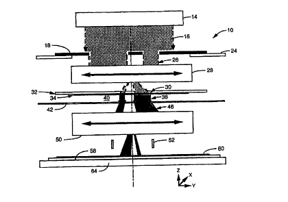
Figure 1 shows in a side view a tandem photon and electron
beam lithography system ("tool")10 in accordance with the
parent application, U.S.S.N. 09/045,728 which includes two
subsystems, the first of 'which is a conventional
photolithography tool, for instance a stepper or scanner, and
the second of which is a demagnifying electron beam column,
where the two subsystems .are coupled by a photoemission
cathode.
A conventional mask 18 (reticle) of the type now used in
photolithography is positioned on a conventional stage 24 which
may or may not be movable along one or both of the depicted x
and y axes, depending on 'the type of photolithography
subsystem. A source of t:he light is for instance a
conventional W light source or a laser illumination system 14
of the type now used in photolithography which provides a
relatively large diameter beam 16 of for instance ultraviolet
(UV) light which passes through the transparent portions of the
mask 18. It is to be understood that the mask is a substrate
transparent to the incident light 16 on which are located
opaque areas. The transparent portions of the substrate define
the image which is to be 'transferred by the mask 18.
Typically, one such mask includes the entire pattern of one
layer of a single integrated circuit die. The mask is usually,
in terms of its X, Y dimensions, some convenient multiple of
the size of the actual di~~ being imaged.
A light optical lens system 28 (which is actually a lens
system including a large :number of individual lens components)
focuses the light 26 passed by the mask 18. The light optical
lens system 28 is either a 1:1 or demagnifying lens system
which demagnifies by e.g. a factor of four or five the image 26
incident thereon to form image 30, which in turn is incident
-5-
CA 02329539 2000-10-20
WO 00/55690 PCT/US00/07060
onto the object. A 1:1 ratio is more advantageous when mask
size is limited. In this case the object, rather than being a
semiconductor substrate, :is the photosensitive backside of a
photoemission cathode 32. The photoemission cathode 32 defines
for instance a minimum feature size of 0.5 micrometers or less,
the minimum feature size of course being dependent upon the
parameters of the system. The photoemission cathode 32 is for
example a thin gold (or oi~her metal) layer deposited on a
transparent substrate.
The photoemission cai:hode 32 (which like the other
elements herein is shown :in simplified fashion) includes a
photoemission cathode layer 34 which absorbs the incident
photons 26 and causes electrons present in the photoemission
layer 34 to be ejected from the layer 34. Some portion of the
electrons 38 which retain sufficient energy to escape from the
photoemission layer 34 arfe emitted into the vacuum portion 40
of the photoemission cathode downstream from the photoemission
layer 34. An electric voltage (typically tens of kilovolts) is
applied to the extraction electrode 42 associated with the
photoemission cathode 32. Extraction electrode 42 extracts the
electrons 38 which have e:~caped from the photoemission layer 34
and accelerates them. Thus the accelerated electrons 46 form a
virtual image of the incident photons 30. In effect then the
photoemission cathode 32 and extraction electrode 42 form a
divergent lens.
There may also be, immediately downstream of the
extraction electrode 42, <~ magnetic (or electrostatic) lens
(not shown) to reduce aberrations. (A magnetic lens is
conventionally a set of coils and magnetic pole pieces, and
yokes which focus the electron beam.) Such an electron beam
system has been found to offer resolution of below 10 nm.
Immediately following (downstream of) this portion of the
system is a conventional Electron optical lens system 50
consisting of one or more elements forming a deflection system
52 (shown only schematically in Fig. 1).
-6-
CA 02329539 2000-10-20
WO 00/55690 PCT/US00/07060
This lens system further demagnifies the virtual image 46
at the writing plane, which is the plane of the principal
surface of the wafer 58 (substrate) by a factor determined to
achieve the desired minimum feature size. For instance, if a
minimum feature size of 0.5 ~m is resolved at the photoemission
cathode, an electron beam. demagnification factor of five times
is needed for a 100 nanom.eter minimum feature size on the
wafer 58. This means that when a total area of approximately 1
mm x 1 mm is exposed on the wafer 58, a total illuminated area
of 5 mm x 5 mm is required on the photoemission cathode
layer 34. Correspondingly for a 4:1 light/optical
demagnification ratio an area of 20 mm x 20 mm is illuminated
on the mask 18, and a 5 mm x 5 mm area is illuminated for a 1:1
ratio. Of course these are merely illustrative parameters.
The total demagnification factor and exposed wafer area
can be varied to achieve the desired minimal feature size. The
wafer 58, including its electron beam resist layer 60, is
typically supported on a stage 64 which is movable in the x and
y axes (optionally also in the z axis), as is conventional.
Other elements of both th.e photo and the electron beam
subsystems which are well known are not shown, but include
positioning measurement systems using for instance laser
interferometry to determine the exact location of the mask on
its stage and the wafer on its stage, vacuum systems, supports
for the stages, various vibration absorption and isolation
mechanisms to reduce environmental effects, and suitable
control systems, all of the type well known in the lithography
field. The deflection system 52 can be used to compensate
for positionary errors due to mask/wafer misalignment,
vibrations, heating and c>ther effects, and would only use very
small deflection amplitudes.
When the photo subsystem is a stepper type system, the
required area on the wafer 58 is exposed with both the mask
stage 24 and wafer stage 64 in a stationary position. Thus
after each single exposure both the mask and wafer stage are
moved (stepped) to the nE:xt location and stopped before another
CA 02329539 2000-10-20
WO 00/55690 PCT/US00/07060
exposure is started. Each exposure could possibly expose a
single die area on the wafer 58, but field size limitations
would usually require a die to be composed using several steps.
In the case of a scanner, both the mask stage 24 and the wafer
stage 64 move at constant velocities in the ratio of the
demagnification utilized and the exposure is continuous, as is
well known for scanning lithography. The ratio of the stage
velocities is determined conventionally by the total
demagnification factor.
This tandem arrangement shown in Figure 1 can be used to
optically compensate in light optical lens system 28 for
distortions of the electron optical lens system 50. This
allows a larger exposure field, which increase throughput of
the entire system.
Referring now to Figure 2, an embodiment 70 of a tandem
photon and electron beam lithography system illustrating the
ray paths is illustrated. The basic elements of the system 70
are the same or equivalent to the same elements in the tool 10
and the same numerals are utilized for explanation purposes,
although not all the elements are illustrated. The optical
mask 18 can be utilized between the source 14 and the lens
system 28, if desired. The image 30 imposed upon the cathode
32 and the photoemission layer 34 generates the electrons 38,
which are extracted by the extraction lens or electrode 42 to
form the virtual image of the image 30 with the accelerated
electrons 46.
The accelerated electrons 46 form a plurality of diverging
electron beams 72, 74 and 76, each emitting from different
portions of the photocathode 32. The diverging beams 72, 74
and 76 are incident upon an objective lens 78, but in different
locations in the lens 78. The outer beams 72 and 76 thus are
blurred out more than the central beam 74, as they pass through
different outer locations of the objective lens 78.
Referring now to Figure 3, an improved compact tandem
photon and electron beam lithography system of the present
invention is illustrated, designated generally by the reference
_g_
CA 02329539 2000-10-20
WO 00/55690 PCT/US00/07060
numeral 80. Again, the basic elements of the system 80 are the
same or equivalent to the same elements in the tool 10 and the
same numerals are utilized for explanation purposes, although
not all the elements are illustrated. As previously described,
the light image incident upon the cathode 32 generates the
electrons 38 which are acted upon by the extraction electrode
42 to form a plurality of diverging beams 82, 84 and 86.
However, according to the present invention, a field lens 88 is
added to the system 80 between the extraction lens 42 and the
objective lens 78.
The field lens 88 can be a superimposed magnetic or
electrostatic lens, in various configurations, which focus the
divergent beams formed by the electrons 46 into a plurality of
converging beams 84, 84 and 86 which now overlap at the coma
free plane or back focal plane of the objective lens 78. This
causes each of the beams 82, 84 and 86 to pass through the same
location or portion of the lens 78. The outer beams 82 and 86
now are blurred out by the same amount as the center beam 84.
This minimizes field aberrations and fills the objective lens
78 to assure the best resolution and the least image distortion
over a wide imaging field due to the minimal central portion of
the objective lens 78 being utilized. The objective lens 78
then demagnifies the photoemission pattern and focuses a
plurality of image pattern beams 90 onto the resist layer 60
formed on the wafer 58.
The tool 10 with the lens system 50 provides a column
length on the order of fifty (50} to eighty (80) centimeters
(cm) between the electrode 42 and the resist 60. The length of
the column causes additional blurring since the electrons can
interact and interfere with one another as they travel between
the electrode 42 and the resist layer 60. The conventional
system 50 also generally contains four (4) lenses.
The placement of the field lens 88 closely adjacent the
electrode 42, provides a very compact column on the order of
ten (10) to thirty (30) cm. The compact column 80 of the
present invention provides a decreased column length of at
_g_
CA 02329539 2000-10-20
WO 00/55690 PCT/US00/07060
least a factor of two (2) to three (3) times that of the tool
10. This provides a sharper beam focus, with much less
electron-electron interactions. This provides both a faster
writing and a smaller feature size for the system 80.
The deflection system 52 (not illustrated) optionally can
be located between the two lenses, 78 and 88. The system 52
also can include elements. on both sides and as a portion of the
objective lens 78.
Referring now to Figure 4, a further enhanced
demagnification system embodiment is designated by the
reference numeral 100. T'he system 100 provides through the
objective lens 78 a demagnification factor of about five (5).
To obtain a feature size of one tenth (0.1) microns will
require a system demagnification on the order of ten (10).
In the system 100, a plurality of electron beams 102 again
are generated from the extraction electrode 42. However, the
beams 102 are formed into converging beams by the field lens
88, which are focused through a beam-limiting aperture 104 onto
a demagnification lens 106. The demagnification lens 106 forms
a plurality of beams 208 which form an intermediate image 110
and then are focused on the objective lens 78, like the system
80. The objective lens 78 then focuses a plurality of image
beams 112 onto the wafer 58 to form the image as before
described.
As the field size increases, the aberrations due to the
divergent action of extraction electrode 42 become excessive.
These aberrations are too large to allow less than one hundred
(100) nanometer resolution to be achieved. These aberrations
are greatly reduced by utilization of the field lens 88 located
closely adjacent the extraction electrode 42. The lens 88
focuses substantially all off-axial rays 46 at an optimum point
near the center of the objective lens 78.
The resulting design utilizing the field lens 88 and the
objective lens 78 maximizes the effective size of the pattern
30, which can be utilized, while minimizing the length of the
column and substantially reducing distortion and off axis
-10-
CA 02329539 2000-10-20
WO 00/55690 PCT/US00/07060
aberrations, such as astigmatism and coma. The reduction in
the electron-electron interactions, due to the shorter column
length, allows the total system beam current to be increased,
hence increasing the throughput of the field lens systems 80
and 100.
Referring now to Figures 5A, 5B and 5C, additional field
lens embodiments of improved compact tandem photon and electron
beam lithography systems of the present invention are
illustrated.
In Figure 5A, a triode field lens configuration or system
is illustrated, designated generally by the reference numeral
120. The image 30 is illustrated as focused onto the
photocathode 32. To minimize the field lens aberrations in
this configuration, the photocathode 32 is maintained at a
negative accelerating voltage and an anode 122 is maintained at
ground potential. The triode configuration includes another
electrode 124, positioned between the photocathode 32 and the
anode 122. The electrode 124 is maintained at a negative
accelerating voltage which is lower than the voltage on the
photocathode 32, to form a beam crossover focused at a location
126 adjacent the objective lens 78. The location of the
crossover focusing point can be altered by adjusting the shape
as well as voltage of electrode 124.
In Figure 5B, a tetrode field lens configuration or system
is illustrated, designated generally by the reference numeral
I30. The configuration 1.30 is very similar to the system 120,
but with the addition of an another focusing electrode 132 to
independently control the position of the crossover location
126.
In Figure 5C, a magnetic field lens configuration or
system is illustrated, designated generally by the reference
numeral 140. The configuration 140 utilizes only the single
anode 122, combined with a conventional or snorkle type of
magnetic lens 142 to position the crossover 126 location. The
systems 130 and 140 allow a higher field strength to be applied
to the photocathode 32, tlnan the system 120, thus allowing
-I1-
CA 02329539 2000-10-20
WO 00/55690 PCT/US00/07060
higher image resolution. The system 120, however, might have
the lowest distortion of the three configurations.
Although illustrated. in FIG. 1, utilizing an optical mask
18, the source 14 also can be a laser pattern generator, such
as disclosed in U.S. Patent Nos. 4,796,038 and 5,386,221. In
these cases, the pattern is generated directly at the cathode
32, without the use of the mask 18.
Although the present invention has been described with
reference to particular embodiments, the described embodiments
are examples of the present invention and should not be taken
as limitations. As will be appreciated by those skilled in the
art, various other adaptations and combinations of the
embodiments described herein are within the scope of the
present inventions as defined by the attached claims.
-12-