Note: Descriptions are shown in the official language in which they were submitted.
' CA 02329669 2000-12-27
t.. 1
ELECTRICAL CONTACT WITH ORTHOGONAL CONTACT ARMS AND
OFFSET CONTACT AREAS
BACKGROUND OF THE INVENTION
1. Field of the Invention
The present invention relates to electrical contacts and,
more particularly, to an electrical contact with
orthogonal contact arms and offset contact areas.
2. Brief Description of Earlier Developments
U.S. Patent 5,711,690 discloses a card edge connector
having an electrical contact with two orthogonally bent
contact arms and offset contact areas between the two
arms. U.S. Patent 9,607,907 discloses an electrical
contact with generally parallel,; but offset contact
portions which overlap in a path of insertion of a male
l5 pin between the two contact areas. A problem with
conventional electrical contacts which are intended to
receive a mating male contact is that contact arm
deflection can vary too much to be efficiently used in
electrical correctors with very small spacings or pitch
between contacts. In addition, insertion forces of a
male contact between two contact arms in a very small
contact pitch connector cannot be too large, which might
result in damage to the contacts, but contact wipe
between the contacts and contact force between. the
contacts needs to be sufficient to establish a good
electrical mating between the contacts. Thus, there is a
need for an electrical contact which can be used in very
small contact pitch connectors which has good contact
wipe characteristics, relatively low mating force
CA 02329669 2000-12-27
w/
..
' characteristics, and good electrical contact with a
mating male contact.
SUMMARY OF THE INVENTION
In accordance with one embodiment of the present
iinvention, an electrical contact is provided comprising a
first contact arm having a first contact area; and a
second contact arm having a second contact area. The
first and second contact arms form a male contact
receiving area therebetween. The first and second
contact arms are generally orthogonal to each other with
a relatively narrow side edge of the first contact arm
forming the first contact area and facing a relatively
wide side face of the second contact arm which forms the
second contact area.
In accordance with another embodiment of the present
invention, an electrical contact is provided comprising a
first connection section for connection to a first
electrical component; and a second connection section,
connected to the first connection section, for connection
to a second electrical component. The second COIIIIeCtiOn
section comprises two contact arms forming a male contact
receiving area therebetween. The~,two contact arms each
have a male contact contacting area which are
longitudinally offset from each other along a path of
insertion of the male contact into the contact receiving
area. Before the male contact is inserted into the
contact receiving area, the two contacting areas overlap
each other through the path of insertion of the male
;ontact .
;0 In accordance wittn one method of the present invention, a
method of manufacturing an electrical contact is provided
CA 02329669 2000-12-27
i,
3
comprising steps of providing a one-piece member with a
first section having two contact arms; forming a first
contact area on a first relatively narrow face of a first
one of the contact arms, and a second contact area on a
S second relatively wide face of a second one of the
contact arms; and bending the one-piece member to locate
the two contact arms into a general orthogonal position
relative to each other such that the first and second
faces are located opposite each other and form a male
contact receiving area therebetween.
BRIEF DESCRIPTION OF THE DRAWINGS
IS
The foregoing aspects and other features of the present
invention are explained in the following descriptlOIl,
taken in connection with the accompanying drawings,
wherein:
ii
Fig. 1 is a perspective view of fan electrical contact
incorporating features of the present invention;
Fig. 2 is an enlarged perspective view of one end of the
contact shown in Fig. l;
Fig. 3 is a side elevational view of the front end of the
contact shown in Fig. 2;
Fig. 9 is a front elevational view of the contact shown
in Fig. 1;
Fig. 5 is a side elevational view of the front end of the
contact as shown in Fig. 3 with a male contact inserted
between the two contact arms;
CA 02329669 2000-12-27
4
Fig. 6 is a cross-sectional view of the end of the
contact shown in Fig. 1 taken along line 6-6;
Fig. 7 is a perspective view of one embodiment of an
electrical connector comprising the electrical contact
shown in Fig. l;
Figs . 8A and 8B are perspective views of a module having
the contact shown in Fig. 1 and used to form '.the
COnIleCtor shown in Fig. 7;
Fig. 8C is an exploded perspective view of the module
shown in Figs. 8A and 8B; and
Fig. 8D is a partial enlarged perspective view of one
corner of the module shown in Figs. 8A and 8B.
DETAILED DESCRIPTION OF THE PREFERRED EMBODIMENT
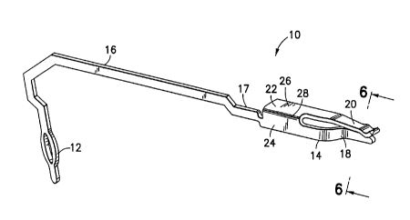
Referring to Fig. 1, there is shown a perspective view of
an electrical contact 10 incorporating features of the
present invention. Although the present invention will
be described with reference to the single embodiment
shown in the drawings, it should be uizderstood that the
present invention can be embodied in many alternate forms
of embodiments. In addition, any suitable size, shape or
type of elements or materials could~be used.
The contact 10 generally comprises a first connection or
mounting section 12, a second connection or mating
section 14, and a middle sectlOIl 1G therebetween. In
this embodiment the contact 10 is a one-piece member
preferably stamped and formed from a flat conductive
member, such as from a sheet of copper alloy. However,
the contact could be comprised of more than one member
and/or could be formed in any suitable manner and/or from
CA 02329669 2000-12-27
f ,
., rJ
ally Suitable Stock: material. The first Co1111eCt1o11
section 12 is a press-fit through-hole solder tail.
However, any suitable first connection section could be
provided, such as a surface mount solder tail. The
middle section 16 can have any suitable length and shape.
In this embodiment the middle section 16 has a series of
angled sections to form a right turn shape for use in a
right angle connector, but the middle section could Lave
a straight shape for a vertical or straight connector.
In this embodiment the middle section 16 has a bent
section 17 to locate the middle section 16 a selected
distance from other middle sections 16 of adjacent
contacts 10 in a connector. However, the first
connection sf,ction 12 and the middle section 16 could
IS have ally suitable shape.
The second connection section 19 generally comprises two
ii
contact arms 18, 20 connected to each other by a base 22.
In alternate embodiments the second connection section
could have more than two contact arms . In addition, the
base 22 need not be provided, such as when the contact
arms project directly off of the middle section 16.
Referring also to Fig. 2, in this embodiment the base 22
has a general cross-sectional "L" shape with two sections
24,26 connected to each other at a!90° bend or corner 28.
The first section 24 preferably extends directly from and
parallel with the middle section 16. However, in an
alternate embodiment the second section 26 and/or the
corner 28 could extend directly from the middle section.
The bend 28 could also be more or less than 90°
s0 Referring also to Figs. 3, 4 and 6, the two contact arms
18,20 extend from the base 22 in a general cantilever
fashion. The first contact arm 18 generally comprises,
in series, a section 30 extending from the first section
CA 02329669 2000-12-27
6
24 of the base 22, a bend 32, and a front contact section
39. The second contact arm 20 generally comprises, in
series, a section 36 extending from the second section 26
of the base 22, a bend 38, a section 40, and a front
contact sectlOll 42. The bend 32 in the first arm 18
locates the front contact section 34 of the first contact
arm directly under the section 40 and front contact
section 92 of tine second Contact arm 20. The first aim's
front Contact section 34 generally comprises a top side
99 having a protrusion 96 and a lead-in surface 48. The
sloped surface leads to a male contact contacting area 50
on the protrusion 96. Because of the flat nature of the
stock material (such as sheet metal) which can be used to
form the contact 10, the first arm's front contact
1S section 39 can have a relatively narrow width W,, and a
relatively tall height H,. The second arm 20, on the
other hand, because of the 90° bend 28, has a relatively
wide width W and a relatively short height H_ . In this
embodiment H is equal to W,.
The bend 38 in the second contact arm 20 angles the
section 90 toward the protrusion 46. The second arm's
front contact section 92 generally comprises a formed
cwrved shape with bottom surface 52 having a male contact
contacting area 59. The curvature at the front end 53 of
the bottom surface 52 forms a cam surface to interact
with a mating male contact. The two contacting areas
50,54 are offset from each other by a length L relative
to the insertion path of the male contact through the
front end of the contact 10. The bend 38 in the second
COTltact arm 20 preferably results lIl the second contact
arm 20 being biased or preloaded against the first
contact arm 18. However, in an alternate embodiment a
preload need not be provided. In this embodiment, with
CA 02329669 2000-12-27
J
7
the contact arms 18,20 in the home state shown in Figs.
2-9, the bottom surface 52 of the second contact arm 20
contacts the top surface 49 of the first contact arm 18
on the sloped surface 48. However, any suitable contact
points could be provided. Alternatively, the arms 18, 20
need not contact each other in the home state.
Referring also to Fig. 5, the two contact arms 18,20 are
shown with a mating male contact P, such as a pin. ~The
pin P can be inserted between the two arms 18,20 in a
longitudinal path or direction of insertion I. The pin P
has a height or width D_. As the pin P is inserted
through the front end of the contact 10, it contacts the
surfaces 48,53 and cams the arms 18,20 apart until the
pin P can slide between the two contacting areas 59,50.
IS As seen in Fig. 3, the curvature of the second contact
arm's front contact area 42, and the protrusion 46 and
i
sloped surface 48 on the first contact arm 18 provide an
overlap distance D~ wherein the ~ontactlllg area 54 is
located below the contacting area 50. Thus, the two
contacting areas overlap each other through the intended
path I of insertion of the male contact P between the two
contact arms. When the male contact P is inserted
between the two arms 18, 20, the arms 18, 20 must be moved
relative to each other a combined !distance of D, and D,_.
Thus, the present invention provides an increased beam or
arm deflection; more than a deflection merely equal to
the male contact's width D... As seen in Figure 5, arms
18, 20 engage opposing sides of male contact P.
The orthogonal arrangement of the arms 18,20 also
provides for a more predictable arm or beam deflection
when the male contact P is inserted. The height H1 of the
first contact arm 18 is relatively larger than the height
CA 02329669 2000-12-27
8
' H, of the second contact arm 20. Therefore, the second
arm 20 will deflect more than the first arm 18 when the
male contact P is inserted. The height H1 of the first
arm 18 can be easily selected when the first arm 18 is
initially stamped and formed to provide any suitable
deflection differential between the two arms 18,20. In
one embodiment the first arm 18 could be sized and shaped
to have almost no deflection when the male contact P is
inserted. In alternate embodiments, H~ could be less than
H;~ , or H~ could be equal to H.. However, W~ and H are
preferably constant based upon the thickness of the stock
material. Thus, positioning of the male contact P
between the two arms 18,20 can be more precisely
controlled which can be beneficial in electrical
COIIneCtors with a relatively small contact pitch, such as
1 mm or less.
The present invention also provides another advantage.
By using the relatively narrow side edge 99 of the first
contact arm 18 to form the contacting area 50 a greater
amount of force can be exerted against a smaller area on
the male contact than could otherwise be exerted by the
broader side faces 45. Thus, there is no need to coin a
curvature onto the area 50. The area 50 can be cross-
sectionally flat. However, the area 50 could be coined
if an even higher contact force is desired. The area 54
could also be coined to form a contact curvature if
desired. In this embodiment, edge 44 is a cut or stamped
edge. Thus, it is relatively easy to form the edge 99
with any suitable male contact contacting surface or
00 shape at the same time that arm 18 is being stamp formed.
In the embodiment shown the two arms 18,20 form a general
cross-sectional "T" shaped interface. In the embodiment
shown, the bottom beam is an "edge of stock" feature
CA 02329669 2000-12-27
. .
while the top beam is a formed feature. Although this
orthogonal contact design is a departure from standard
dual opposing beam technology, the overlapping geometry
proves redundant contact points. The combination of D1
and D illustrates the increased deflection created by the
contact beam geometry. This deflection range and
corresponding mating force can be modified to meet the
specific needs of different applications by modifying..the
beam/arm geometry. The contact arms 18, 201 could be
sized and shaped such that forces against the arms,
exerted by an inserted male contact, cancel each other
out. Therefore, total forces on a connector housing in
which the contact is mounted are counteracted. If the
forces on individual contacts do not cancel each other
IS out, each COTltact could be arranged relative to another
contact such that the "T" shaped interfaces are in
opposite positions. Thus, th:e combined forces could
counteract each other.
Referring now to Figs. 7, 8A, 8B, 8C and 8D, one
embodiment of an electrical connector 100 having
electrical contacts incorporate features of the present
invention will be described. In this embodiment the
receptacle 100 generally comprises a housing 102 and a
module assembly 104 connected to 'the housing 102. The
housing 102 generally comprises a first housing member
106 and a second housing member 108. The first and
second housing members 106, 108 are preferably comprised
of a dielectric material, such as a molded plastic or
polymer material. The first housing member 106 includes
a top 110, a back 112, two sides 114, a generally open
front, a generally open bottom, and a receiving area 120.
The top 110 includes module mounting holes 122. The back
112 includes module mounting holes 124. The front
CA 02329669 2000-12-27
includes extensions from the sides 114 for insertion into
and connection with the second housing member 108. The
second housing member 108 includes apertures or lead-ins
through a front face 130 for insertion of front ends of a
5 mating connector's male pins into the connector 100.
The module assembly 109, in this embodiment, generally
comprises six contact modules 132 (one of which is shown
in Fig. 8A) and may include an additional ground member
(not shown). In alternate embodiments more or less than
10 six contact modules could be provided arid, more or less
than one ground member could be provided. In this
embodiment flue contact modules 132 comprise two sets of
two types of contact modules which are preferably mirror
images of eaclu other. The ground member is sandwiched
IS between the two sets. Each contact module 132 generally
comprises a frame 190, signal contacts 192, and ground
I I
contacts 149. The frame 190 is preferably comprised of
dielectric material, such as molded plastic or polymer.
The frame 140 comprises a top side 146, a bottom side
198, a rear side 7.50, a front side 152, and two lateral
sides 154, 156. The top side 146 includes a latch 158.
The latch 158 is inserted into one of the module mounting
holes 122 to connect the contar_t module 132 to the first
housing member 106. The rear side 150 also includes a
projection 160. The projection 160 is inserted into one
of the module mounting holes 129 to connect the module
132 to the first housing member 106. The frame 140
includes channels 162 along at least one of the sides 159
for receiving portions of the ground contacts 144. The
frame 190 could also have channels for receiving portions
of the signal contacts 192. However, the frame 190 is
preferably over-molded onto portions of the signal
contacts 192. Alternatively, or additionally, the frame
CA 02329669 2000-12-27
11
19U could be over-molded onto portions of the ground
contacts 144. The front side 152 of the frame 140
includes pockets 169 and receiving area 165.
In this embodiment each contact module has six of the
S signal contacts 192; three as a first type 142a of signal
contacts and three as a second type 192b of signal
contacts. The signal contacts 142 each have a first end
166, a middle section 168, and a second end 170. ~~The
first ends 166 have through-hole solder tails, but any
suitable first ends could be provided, such as surface
mount solder tails. The middle sections 168 all have
right turn shapes, but with different lengths or
dimensions to allow the signal contacts to be aligned in
a row or common plane. The second ends 170 each comprise
two deflectable arms 172, 174 oriented 90'' offset from
each other. The arms 172, 174 in the first type of
signal contact 142a are orientated as mirror images of
the arms 172, 179 in tine second type of signal contacts
192b. The signal contacts 192 generally incorporate
features of the contact 10. More specifically, the
second ends 170 are structured similar to the second
connection section 19 with the arms 172, 174
corresponding to the arms 18, 20. The signal contacts
192 can have the bend 28 in the upper left hand corner,
the upper right hand corner, the lower left hand corner
or the lower right hand corner of the second ends 170.
Preferably the arms 172 (equivalent to arm 20) are
located on only the top or bottom of the second ends 170
(as illustrated in Fig. 8C) and the arms 174 (equivalent
i0 to arm 18) extend from either the right side or the left
side depending upon which one of the six contact modules
132 they are in. In alternate embodiments other types or
orientations of the second ends could be provided.
~
CA 02329669 2000-12-27
12
'lhe ground COIltacts 144 for each module 132 can be
provided as a single one-piece member or multiple members
as shown. Each ground contact 144 includes a first end
176, a middle section 178, and a second end 180. The
S first ends 176 have through-hole solder tails. However,
any suitable types of first ends could be provided, such
as surface mount solder tails. The middle sections 178
generally comprise first sections 182 and second sections
184. The first sections 182 are located in the slots 162
of the frame 109 to fixedly connect the ground contacts
194 to the frame 190. The second sections 184 extend
along the side surfaces 154 of the frame 190. The middle
sections '178 have a general right turn shape such that
tOe two ends 176, 180 are at a general right angle to
1S each other. However, any suitable shape of the middle
sections could be provided. The second ends 180 include
three different types of second; ends. The first type of
second end has a slot at a corner; with a top arm and a
side arm on opposite sides of the slot. The deflectable
?0 projections extend from the arms. The second type of
second end is generally a mirror image, of the first type
of second end. The third type of end has two slots at
two corners with a top arm, a bottom arm and a side arm.
Two deflectable projections extend into the first slot,
2_S and two deflectable projections extend into the second
slot. The side arm also includes a third slot. However,
in alternate embodiments, any suitable types) of second
ends could be provided.
Referring now also to Fig. 8D, a partial enlarged view of
30 the front end of one of the modules 132 is shown. The
two arms 172, 174 of each second end 170 of the signal
contacts 192 are located in front of one of the pockets
164. A signal pin from a mating connector, when inserted
CA 02329669 2000-12-27
13
' tlorougln oue of floe lead-ins of the housing, extends
between the two arms 17a, 174 into the pocket 164. The
arms 172, 179 resiliently deflect outward. The slots 186
of the ground contacts 149 are located at the receiving
areas 165 of the modules' frame 140. A ground pin from
the mating connector can extend into the slot 186 and
receiving area 165 between the two projections 192, 194.
When the module assembly 104 is assembly the ground
contacts 149 and the ground member 134 combine to
effectively surround the signal contacts to form an
electromagnetic shielding for the signal contacts. The
ground member 139 also has a front end for connection to
ground pins from the mating connector.
It should be understood that the foregoing description is
IS only illustrative of the invention. Various alternatives
and modifications can be devised by those skilled in the
art without departing from the invention. Accordingly,
the present lIlVention is intended to embrace all such
alternatives, modifications and variances which fall
within the scope of the appended claims.