Note: Descriptions are shown in the official language in which they were submitted.
.. CA 02329727 2000-10-20
1
BIDIRECTIONAL OPTICAL WAVELENGTH
MULTIPLEXER AND DEMULTIPLEXER
Technical Field
s The present invention relates to a bidirectional optical wavelength
multiplexer and demultiplexer, and a bidirectional optical wavelength
multiplexer and demultiplexer which multiplexes and demultiplexes light.
Background Art
,o General optical wavelength multiplexer/demultiplexers using an arrayed
waveguide grating (hereinafter, referred to as AWG), which essentially apply
the principle of Mach-Zehnder Interferometer, multiplex and demultiplex light
using the phase difference.
FIG. 1 is a structure view of a conventional optical wavelength
,s multiplexer and demultiplexer. Referring to FIG. 1, a conventional optical
wavelength multiplexes and demultiplexer includes N first arrayed waveguides
100 connected to an optical fiber for receiving light having different
wavelengths, a first planar waveguide region (free space region, slab
waveguide, or star coupler) 102 for distributing received light, an AWG 104
for
~o allowing light from the first planar waveguide region 102 to have different
phase differences, a second planar waveguide region 106 in which the light
having different phase differences output from the AWG 104 interfere with
each other and land at different locations on the opposite side according to
wavelength, and M second arrayed waveguides 108 for outputting the light
2s split according to wavelength.
This operation of the optical wavelength multiplexer/demultiplexer can
be explained in a grating equation which describes the dispersion
characteristics of an AWG which acts as a diffraction grating with respect to
incident light.
3o In the grating equation, the phase changes caused in the first planar
CA 02329727 2000-10-20
2
waveguide region 102, the AWG 104 and the second planar waveguide region
106 are all summed, and the sum of the phase changes satisfies the condition
in which interference occurs at the interface between the second planar
waveguide region 106 and the second arrayed waveguides 108. The grating
s equation is expressed with respect to light received via an input waveguide,
as
in Equation 1:
nsd sing + n~~L= m~. ...(1)
wherein ns denotes the effective refractive index of a planar waveguide
region,
n~ denotes the effective refractive index of an AWG, d denotes the pitch of an
AWG, m denotes the diffraction order, DL denotes the length difference
between adjacent AWGs, and ~ denotes the wavelength of the incident light.
A central operating frequency Ao is the wavelength when 8 is zero, and
is defined as in Equation 2:
n~~L = mho ...(2)
Equation 3, which describes a variation in angular dispersion, that is, a
variation in the diffraction angle of light with respect to a change in
~s wavelength, can be obtained from Equation 1:
d8 nz
d~. nsd
That is, light beams having different wavelengths land at different
angles on the second planar waveguide region of an optical wavelength
multiplexer/demultiplexer, according to Equation 3. Thus, an output
waveguide is connected at a location corresponding to the diffraction angle of
light having a wavelength used in the second planar waveguide region, and
thus performs optical wavelength demultiplexing with respect to the
wavelength.
A general optical wavelength multiplexer/demultiplexer using the
CA 02329727 2000-10-20
3
structure of an AWG has a structure in which the left side and the right side
are symmetrical to each other, so that the same function is performed
independently of the direction of connectiowof the device. Also, in the
general
optical wavelength multiplexer/demultiplexer having a symmetrical structure,
s input and output waveguides have no difference in structure, so that an
arrayed waveguide can act as an input waveguide or an output waveguide
according to the direction of connection.
This optical wavelength multiplexer/demultiplexer can only operate in
one direction at one time, so that there is a method for allowing the optical
wavelength multiplexer/demultiplexer to operate having different channel
intervals according to the state of connection of the device by
differentiating
the intervals between first and second arrayed optical waveguides. However,
this method is also the same as the conventional method in that an arrayed
waveguide acts as an input or output waveguide according to the direction of
~s connection of the device.
Also, when this optical wavelength multiplexer/demultiplexer is applied
to a real system, it is commonly installed and used in only one direction.
Therefore, the manufacture of an optical wavelength multiplexerldemultiplexer
which can operate with the same operation characteristics in two directions
2o cannot be a necessary condition for designing an optimized device that
satisfies a given specification.
Disclosure of the Invention
An objective of the present invention is to provide a bidirectional optical
2s wavelength multiplexerldemultiplexer which can simultaneously multiplex and
demultiplex light by connecting a central waveguide at the interface between
each planar waveguide region and an arrayed optical waveguide.
To achieve the above objective, the present invention provides an
optical wavelength multiplexer/demultiplexer including an optical waveguide
3o array having a plurality of optical waveguides, a planar waveguide region
CA 02329727 2000-10-20
4
connected to the optical waveguide array, and an arrayed waveguide grating
connected to the planar waveguide region, wherein the optical waveguide
array further includes a central waveguide formed at a location-on which light
transmitted from the arrayed waveguide grating to the planar waveguide
s region is focused, on the interface between the optical waveguide array and
the planar waveguide region, and light multiplexed with a plurality of
wavelengths is received or output via the central waveguide.
Brief Description of the Drawincts
,o FIG. 1 is a structure view of a conventional optical wavelength
multiplexer/demultiplexer;
FIG. 2 is a structure view of a bidirectional optical wavelength
multiplexer/demultiplexer according to the present invention;
FIG. 3 shows the central waveguide of FIG. 2;
~s FIG. 4 shows a bidirectional optical wavelength demultiplexer using
FIG. 2;
FIG. 5 shows a bidirectional optical wavelength multiplexes using FIG.
2; and
FIG. 6 shows a bidirectional optical wavelength
2o multiplexer/demultiplexer using FIG. 2.
Best mode for carryings out the Invention
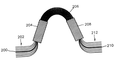
Referring to FIG. 2, an optical wavelength multiplexerldemultiplexer
according to the present invention includes a first waveguide array 202 having
2s a first central waveguide 200, a first planar waveguide region 204, an
arrayed
waveguide grating (AWG) 206, a second planar waveguide region 208, and a
second waveguide array 212 having a second central waveguide 210. Here,
the first central waveguide 200 is formed at the focus (F1 ) on the interface
between the first waveguide array 202 and the first planar waveguide region
204. The focus F1 is a location on the first planar waveguide region 204
CA 02329727 2000-10-20
where light from the AWG 206 is focused. The second central waveguide 210
is formed at the focus (F2) on the interface between the second planar
-- waveguide region 208 and the second waveguide array 212. The focus F2 is
a location on the second planar waveguide region 208 where light from the
s AWG 206 is focused.
FIG. 3 shows the relationship between the central waveguide and the
planar waveguide region of FIG. 2. Here, reference numeral 300 is an AWG,
reference numeral 304 is a planar waveguide region, reference numeral 306 is
an optical waveguide array having 8 waveguides, reference numeral 308 is a
central waveguide formed at the focus F2, and reference numeral 302 denotes
the interface between the AWG 300 and the planar waveguide region 304.
The interval between optical waveguides connected to a planar
waveguide region denotes the interval of the wavelengths of an output
spectrum. The central waveguide, which is the feature of the present
~s invention, must be connected to a location that is independent of the
locations
corresponding to the wavelengths of light transmitted by a plurality of
optical
waveguides that pertorm a general multiplexing/demultiplexing function. Here,
the central waveguide is connected to the substantial focus on a planar
waveguide region.
2o FIG. 4 illustrates an example in which a bidirectional optical wavelength
multiplexer/demultiplexer according to the present invention operates as a
bidirectional optical wavelength demultiplexer. When light having a
wavelength of ~~o A~~ is input to the first central waveguide 200 in the first
waveguide array 202, and simultaneously light having a wavelength of ~;0 1~;~
is
Zs input to the second central waveguide 210 in the second waveguide array
212,
the light having a wavelength of ~~o ~~~ is output via the other waveguides in
the
second waveguide array 212, and the light having a wavelength of ~;o A;,yis
output via the other waveguides in the first waveguide array 202. That is,
when multiplexed light having several wavelengths is received via the central
3o waveguide formed within each of the first and second arrayed waveguides,
CA 02329727 2000-10-20
6
light received via the central waveguide within an arrayed waveguide is
demultiplexed by wavelengths and output via a plurality of waveguides within
an arrayed waveguide opposite to the arrayed waveguide which has received
the multiplexed light.
To be more specific, when light having several wavelengths is received
via the first central waveguide 200, the first planar waveguide region 204
distributes the received light, and the AWG 206 allows light beams from the
first planar waveguide region 204 to have different phase differences. The
second planar waveguide region 208 causes interference between light beams
having different phase differences, which are output from the AWG 206, and
outputs light beams of different wavelengths via different waveguides within
the second waveguide array 212. Likewise, when light having several
wavelengths is received via the second central waveguide 210, lights of
different wavelengths are output via different waveguides within the first
~s waveguide array 202.
When the central waveguide in the bidirectional optical wavelength
multiplexer/demultiplexer according to the present invention is only used as
an
input waveguide, it is preferable that an optical isolator is connected to the
input-dedicated waveguide in order to prevent interference or a return loss
due
2o to output light.
FIG. 5 illustrates an example in which a bidirectional optical wavelength
multiplexer/demultiplexer according to the present invention operates as a
bidirectional optical wavelength multiplexer. When light beams of different
wavelengths A;o A;7 are received by the waveguides (except for the first
central
2s waveguide 200) of the first waveguide array 202, they are multiplexed and
output via the second central waveguide 210. Likewise, when light beams of
different wavelengths ~~o A~~ are received by the waveguides (except for the
second central waveguide 210) of the second waveguide array 212, they are
multiplexed and output via the first central waveguide 200.
3o FIG. 6 illustrates an example in which a unidirectional optical wavelength
CA 02329727 2000-10-20
7
multiplexer/demultiplexer according to the present invention operates as a
bidirectional optical wavelength demultiplexer. When light having different
wavelengths ~~o ~~~ is received by the first central waveguide 200 of the
first
waveguide array 202, and light beams of different wavelengths ~;0 7~;~ are
s received by the remaining waveguides, the light beams of different
wavelengths
~;o ~;, are multiplexed and output via the second central waveguide 210, and
the
multiplexed light having different wavelengths ~~o A~~ is demultiplexed and
output
via the waveguides (except for the second central waveguide 210) of the
second waveguide array 212.
,o It is preferable that an output waveguide is selectively connected to an
optical fiber in a packaging step in order for this bidirectional optical
wavelength multiplexer/demultiplexer to have different channel intervals in
two
directions. The configuration or designing variables of a conventional optical
wavelength multiplexerldemultiplexer can be used as those of the device in a
,s chip step.
Industrial Ap~~licability
As described above, according to an optical wavelength
multiplexer/demultiplexer according to the present invention, a central
2o waveguide, through which multiplexed light is received and output, is added
together with a plurality of optical waveguides, at a place where the output
spectrum of these waveguides are not affected, so that the multiplexed light
can be demultiplexed in a direction from an optical waveguide array on one
side to an optical waveguide array on the other side, and simultaneously
2s demultiplexed light can be multiplexed in a direction opposite to the above
direction.