Note: Descriptions are shown in the official language in which they were submitted.
r
CA 02330169 2001-O1-02
WIDE WORD MULTIPLIER USING BOOTH ENCODING
The present invention relates to the field of arithmetic processors and more
particularly to
a method and circuit for multiplying large numbers using a booth encoder with
iterative
addition.
BACKGROUND OF THE INVENTION
As is well known multiplication of two numbers can be performed by a series of
repeated
additions, where the number to be added is the multiplicand and the number of
times that
it is added is the multiplier, the result is the product. Each step in the
series of repeated
additions generates a partial product. As it may be well appreciated, this
process may be
extremely slow when performed in a general-purpose processor, taking many
clock
cycles. In general terms multiplication of an M-bit number by an N-bit number
will
result in a product which is M + N bits long.
The increased need for high speed processing of large numbers has been
precipitated by,
for example, various cryptographic applications that use large numbers as
encryption
keys. These keys are at least 1024-bits long. Accordingly, multiplication
using the
repeated addition method that is suggested by the arithmetic definition above
is often
replaced by more efficient algorithms that make use of positional number
representation.
In general, the execution speed of an arithmetic operation is a function of
two factors.
One is a circuit technology and the other is the algorithm used.
The multiplication operation may be thought of as having two parts. The first
part is
dedicated to the generation of partial products and the second one collects
and sums the
partial products to obtain the final result. The booth algorithm is often used
in the
generation part because it reduces the number of partial products. The
collection of the
partial products can then be made using a regular array, a Wallace tree or a
binary tree.
For an N-bit multiplier, no more than N/2 partial products are created.
However, when
the partial products from one multiplier operation are first added, the result
is initially in a
redundant format, such as carry-sum. That is, the result takes the form of two
rows of
I
r
CA 02330169 2001-O1-02
binary information, a carry row and a sum row. But before this result may be
used again,
it must first be processed by an adder to put it into binary format. In other
words, the
carry row and the sum row must be added first. As mentioned earlier a Wallace
tree
compression unit also known in the art may be used to take the partial
products and using
rows of carry-save adders compress the partial products into two rows, a sum
row and a
carry row. A conventional N-bit full adder may then be used to add the sum row
and the
carry row.
However this full adder is slow since a carry generated in the low order bits
may ripple
all the way through to the high order bits. Thus the high order must wait for
the carry to
ripple through all N-bits. This problem is exacerbated when large width
operands are
used. Alternatively, carry look-ahead and carry select adders may be used to
avoid large
propagation delays, but are still slow. The complexity of such adder circuits
is directly
related to the width of the adder. A 32-bit adder is reasonable to implement
using most
technologies. A 64-bit adder is extremely large, extremely slow or both.
United States patent No. 5,944,776 describes one possible approach to
eliminating the
need for a full adder; by using a multiplicity of interconnected logic cells
that produces a
Booth output that is the Booth encoded form of the sum of a sum row and a
carry row.
This technique is not easily adaptable to wide width operands. Furthermore the
technique
described by this patent is more applicable to iterative multiplication
algorithms used in a
multiplicative divider.
In United States Patent number 5,724,280 a Booth multiplier using carry look
ahead
adders performs a multiplication operation in three stages: First the operands
are loaded
from a data bus, which takes a minimum of 8 clock cycles for a 256 -bit
operand and a 32
bit bus; second while loading the second operand, Booth encoding is begun 4-
bits at a
time and encoded values are accumulated, which takes 64 clock cycles; and
third
performing a final addition on 32-bit segments while outputting a result to
the data bus,
which requires 8 further clock cycles when using a 32-bit adder and a 32-bit
data bus.
Hence, a total number of 80 clock cycles are needed with a 32-bit data bus and
a 32-bit
2
s
CA 02330169 2001-O1-02
adder. This circuit would thus be unacceptably slow when used with wider width
operands.
It is possible to implement a high speed wide-width multiplier (256-bit by 256-
bit) by
using a number of 256-by-256 Booth multipliers which are pipelined to obtain
the desired
speed. But, such a circuit would be impractically large, particularly for
implementation in
an ASIC.
Furthermore, wide-width numbers can be processed by segmenting the operands
and
processing each of the segmented operands in a multiplier. The results from
the
processed segments are combined to obtain a final result. A problem associated
with this
technique is that carries generated while processing each segment have to be
properly
processed in order to obtain the correct final result, thus placing a
constraint on the adder
circuit, used to combine the results.
It is thus desirable to have a multiplier circuit using Booth encoding that
performs wide
width number multiplication in relatively few clock cycles and which occupies
minimal
chip area. Furthermore it is also desirable to have a more efficient adder
circuit for
processing the final result from the Booth encoder and which manages the
carries
generated in the Booth multiplier.
SUMMARY OF THE INVENTION
In accordance with this invention there is described a multiplier for
computing a final
product of a first operand and a second operand comprising:
(a) a multiplier array for forming a product of the first operand and second
operand in
carry-save form;
(b) a carry-save adder for adding said carry-save partial products and an
accumulatd sum
to produce a carry and save values;
(c) a carry-lookahead adder for adding said carry and save values to produce a
product
value and a carry-out value;
(d) a general purpose adder for adding said carry-out and said product value
to
produce said final product.
CA 02330169 2001-O1-02
BRIEF DESCRIPTION OF THE DRAWINGS
The invention will now be described in conjunction with the attached drawings
in which:
Figure 1 is a block diagram of an arithmetic logic unit (ALU) incorporating a
multiplier
according to the invention;
Figure 2 is a block diagram of a general-purpose adder according to the
present
invention;
Figure 3 is a block diagram of a multiplier according to an embodiment of the
invention;
Figure 4 is a block diagram of an Iterative Adder used in the multiplier of
figure 3;
Figure 5 is a timing diagram for the multiplier of figure 3;
Figure 6 is a schematic diagram illustrating the steps involved in performing
Booth
multiplication using iterative addition;
Figure 7(a) is a diagram of a multiply operation illustrating errors resulting
from obvious
implementation approaches;
Figure 7(b) is a table showing the effect of simple sign extension ;
Figure 8 is a symbolic representation of a multiply operation for use in
illustrating
problems and potential solutions thereto;
Figure 9 is a flow diagram showing sign extension as applied in the multiplier
of the
present invention; and
Figure 10(a) is an example showing sign extension applied to each SUM results
from
employing a path from flowchart in Fig. 9; and
Figure 10(b) is an example based on data shown in Fig. 7 showing sign
extension applied
to each SUM results from employing a path from flowchart in Fig. 9.
DETAILED DESCRIPTION OF THE INVENTION
4
i
CA 02330169 2001-O1-02
In the following description, like numerals refer to like elements in the
drawings.
Large numbers are frequently used, in many different applications, such as in
cryptographic applications, and are typically in the order 1024-bits long or
greater.
Although a multiplier circuit of this size is possible theoretically,
practically it is not
feasible given today's technology. Therefore, a 1024x 1024 multiply operation
must be
implemented using plural smaller multiplier circuits such as 256-bit
multiplier. A method
for multiplying large numbers, with a multiplier circuit that is capable of
multiplying two
256-bit numbers is described as follows. Assuming one is to multiply two 1024-
bit
numbers. Each number is sub-divided into four successive 256-bit segments.
Multiplication is performed on the segments using the fixed width multiplier
circuit to
form partial products of the segments. The partial products of the segments
are then
concatenated, and shifted versions of the partial products are accumulated to
yield the
final product of the two large numbers. The present invention provides a
multiplier
circuit and method for performing a wide multiplication of such numbers in a
minimum
number of clock cycles. For example a 256-by 256-bit multiply operation is
performed in
typically about 11 clock cycles.
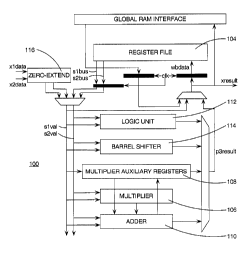
Referring to Figure 1, a block diagram of an arithmetic logic unit (ALU)
incorporating a
multiplier according to an embodiment of the present invention is shown
generally by
numeral 100. The ALU includes a pair of 256-bit internal data paths (slval,
s2val) for
carrying data and information between its various components and a control CPU
(not
shown). The components of the ALU include a 256-bit register file 104 for
holding
operands and results from computations, a 256-by-256-bit Booth multiplier 106
for
performing wide-width multiplication, an auxiliary register 108 for holding
the
intermediate results of the multiplication, and a general-purpose adder 110
for processing
an output from the Booth multiplier with intermediate output results stored in
the
auxiliary register to produce a final output result which is written into the
register file 104
or an intermediate result which may be written back into the auxiliary
register 108. The
general-purpose adder 110 is also coupled to the data path to perform addition
or
subtraction on operands received directly along the data path. A zero-extend
block 116 is
also provided to prepend zero's to 32-bit data or instructions to 256 bits.
5
r
CA 02330169 2001-O1-02
It may be noted that the operation of the ALU is generally controlled by the
control CPU
and data is transferred between the ALU and global RAM under control of the
CPU.
Further as shown in figure l, the ALU includes a logic unit 112 and a barrel
shifter 114,
however these components are well known to those skilled in the art and not
involved in
the multiplication operation and therefore will not be discussed further.
Each of the components of the ALU 100 will be described in greater detail
below,
followed by a detailed description of their operation.
The auxiliary register 108 comprises two 256-bit product registers PLO for
storing the
least significant 256 bits, PHI for storing the most significant 256 bits and
an 8-bit
product overflow register (POV). A 256-bit path carries data between the
auxiliary
register 108 and the general-purpose adder 110. In addition, the auxiliary
registers are
coupled to receive data from the data path.
The register file 104 consists of sixteen 256-bit registers. Each register has
two read
ports and one write port.
Refernng to figure 2 there is shown a block diagram of the general-purpose
adder 110.
The adder 110 is a re-circulating adder, also known as an iterative adder, and
is
comprised of eight 32-bit adders 202, for processing consecutive 32 bits from
the 256-bit
data path slval, s2va1 to each produce a 32-bit result. These 32-bit adders
are readily
available and widely implemented. Thus the performance and area of these 32-
bit adders
are well known. A pair of multiplexors 204, 206 are coupled to each 32-bit
adder 202.
One of the pair of inputs to each multiplexor is coupled to the data path to
receive the 32-
bits from either slval or s2val. The other of the input to the multiplexors is
coupled via a
clocked buffer to selectively receive the output from its corresponding 32-bit
adder.
Furthermore, the s2va1 signals are coupled via XOR gates 208 to the
multiplexors 206"
thus for subtraction the XOR gates 208 can be set to invert the s2va1 signals.
A carry out
signal c0,cl,...c6 from respective adders 202 is coupled to a carry-in input
of its adjacent
adder.
6
CA 02330169 2001-O1-02
This adder 110 may be used as a general-purpose adder in the ALU. In order to
add two
values, each of the addends are split into eight 32-bit segments. Each segment
is added in
a corresponding 32-bit adder to produce eight 32-bit partial sums and eight
carry outputs.
If all but the leftmost carry output is zero then the addition is complete.
The sum is
S formed by the concatenation of the eight partial sums, and the carry-out is
the value of
the leftmost carry bit. Otherwise, if carry outputs other than the leftmost
carry are non-
zero, then the partial sums are routed back into one input of the adder, while
the other
input of the adder is set to zero. The carry input of each of the adders is
set to the state of
the carry of its right-hand neighbour and the addition is continued.
In addition to the eight 32-bit adder segments, an 8-bit adder 210 is used to
finish part of
a multiplication operation performed in the multiplier. The 8-bit adder 210
also has its
inputs coupled to respective multiplexors. One of the multiplexors 212 is
coulped to the
POV register, while the other multiplexor 214 has an input coupled to receive
a carry out
signal cout from the multiplier 106. The use of the general-purpose adder in
multiplication will be explained in more detail later.
Refernng to figure 3, a block diagram of the multiplier 106 is shown. The
multiplier 106
performs 256x256-bit multiplication and comprises a well known 257x32-bit
radix-4
Booth encoded Wallace tree array 302, an 8x32-bit carry-lookahead adder 304,
an
overflow detector 306 and a control block 308. In addition the multiplier 106
uses the
auxiliary register 108 (comprised of the three aforementioned register
segments
PHI,PLO,POV) to store results during the multiplication and uses the general-
purpose
adder 110, shown in figure 2 to compute the final product in the
multiplication operation
to clear out any remaining carnes.
Before continuing with a detailed description of the components of the
multiplier, a brief
high-level description of the algorithm used to perform the multiplication is
provided as
follows. This will serve to more clearly understand the interconnection of the
various
components within the multiplier 106.
The 257x32 multiplier array 302 is capable of generating a 288-bit partial
product ( 256
plus 32) in two clock cycles. Thus for a 256x256 multiply, eight rounds of
multiplication
CA 02330169 2001-O1-02
are run, using 32-bit segments of the multiplier, starting with the lowest
order 32 bits. For
a 256x32 multiply, the 32-bit multiplier is used directly, and only one round
is required.
To illustrate the algorithm, consider the multiplication of two 8-digit
decimal numbers
and that an 8-digit x 1-digit multiplier is available, The table below shows
this operation.
The table on the left shows a standard partial product method. The table on
the right,
shows the first four steps of the multiplication to illustrate the intent of
the circuitry that
makes up the multiplier. The multiplicand "31415926" is multiplied by the
first digit of
the multiplier "5" resulting in a partial product "157079630". Note that the
partial
product contains nine digits. In general, the partial product will contain the
number of
digits in the multiplicand plus the number of digits we are using in the
multiplier. Also
note that the least significant digit "0" is never added to anything. It can
be shifted out to
form part of the final product. The remaining digits of the partial product
are shifted right
one position and added to a second partial product. Again, the rightmost digit
"5" of the
resulting sum is not involved in any further computation, so it can be shifted
out. The
remaining digits are shifted right one position, and the process continues.
After the eighth
partial product has been produced, the final sum forms the leftmost digits of
the final
product.
31415926 157079630 ~0
83014375
157079630 15707963
219911482 219911482
94247778 235619445 ~5
125663704
31415926 23561944
00000000 94247778
94247778 117809722 ~2
251327408
2607973461936250 11780972
125663704
137444676 ~6
etc.
8
CA 02330169 2001-O1-02
The multiplier uses a similar algorithm, except that instead of decimal
digits; each
fundamental unit is 32-bits. The multiplicand is 256-bit wide and the partial
products are
288 bits wide.
Accordingly, refrring back to figure 3, the Booth multiplier array 302 takes
in a 257-bit
multiplicand and a 32-bit multiplier, and produces a 289-bit product in carry-
save form
two clock cycles later. (The purpose of the extra bit in the multiplicand and
products will
be explained later.) The output from the Booth multiplier 302 is two numbers
that, when
added together, forms the 289-bit partial product. The shifter unit 114 shifts
the products
left one bit if required. The shift operation's output is one bit wider than
the input, so 290
bits are output from the shifter.
The two partial products p0 and pl from the multiplier 302 are added to a
third value
acc in to form a sum iacc which is latched in a register, since it is routed
to acc in for
subsequent rounds. The addition is performed using a carry-save adder followed
by a
carry-look-ahead adder. The lower-order 32 bits of the sum are correct; they
are written
into the PLO register. The first set of 32 digits are written to PLO[31:0],
the second set
produced on the next round are written to PLO[63:32], and so on.
The adder 304 itself is similar to the 256-bit adder 110 described earlier, in
that it
consists of 32-bit full adders whose carries are latched and re-used on the
next round.
However, the interconnect is different. Since the partial sum must be shifted
right 32 bits
after each round, the carry bits are routed back to the input of the adders
that produced
them. This adder is described in more detail in figure 4. After all multiplier
rounds have
been performed, either one or eight 32-bit results have been produced and
stored in the
PLO register. The remaining bits of the final product are in iacc, however,
the addition is
not "complete" since there are partial carnes still latched in the
multiplier's adder. For a
multiply-accumulate, the value in POV:PH1 still needs to be added in. This
addition,
along with resolution of the carries inside the partial sum iacc, is performed
in the general
purpose adder 110.
y
CA 02330169 2001-O1-02
To reiterate some of the discussion above, referring back to figure 3, two
operands inputs
a(255:0) and b(31:0), along with control signals are applied to the control
block. Though
b is shown as having 32-bits, it could have the full 256-bits with
segmentation performed
in the control block. Alternatively another segment length such as 16 bits or
64 bits can
be used. Preferably, the segment length is a power of two. An accumulated sum
input
acc sum(255:0) is also provided to the control block for accumulation with a
product.
The control signals include a reset signal (reset), a start multiply signal
(start mint), a
multiply accumulate signal (mul acc) for distinguishing multiply accumulate
operations
from simple multiply operations, a clock signal (clk). The control block also
provides
control signals start-add, end add to the adder 304. The control block 308
latches the
operands and control signals and then schedules the whole multiplication
process.
The 256 x 32-bit Booth encoder 302 receives the data from the control block
308 and
generates two partial product values, PO(287:0) and P 1 (287:0).
The Overflow Detector block 307 is coupled to the Booth encoder 302 block to
identify
if any of PO or P1 is a negative quantity and provide an over flow signal 312
to the
adder block 304 for determining the value with which to pad the highest order
segment
(as will be described later).
The adder 304 has partial product inputs (P0, P 1 ); an accumulated sum input
(acc sum);
and an accumulated carry input (acc carry. The operation of which will be
described in
figure 4. T'he adder block 304 outputs a carry out value (cout) 314, and a
signal
indicating completion of the multiplication operation (mint done) 316 and a
product
output product(287:0) 318.
Figure 6 illustrates conceptually the operation of the multiplication
algorithm using
Booth encoding with Wallace tree partial product reduction and iterative
addition . The
multiplier 106 receives two operands A and B, and generates the product of A
and B
product (287:0). For example, if both A and B are 256-bits wide, a single
256X256
Booth multiplier can be designed to meet a predetermined operating frequency.
Unfortunately, such a circuit is impracticably large, requiring encoding of
two 256-bit
numbers into two 512-bit numbers. Hence, B is segmented into eight 32-bit
chunks,
to
CA 02330169 2001-O1-02
B(0), B(1), ... , B(7). A 256X32 Booth multiplier can be implemented in a
practical
amount of space, for example, for an ASIC. In order to perform the
multiplication of the
256-bit multiplicands, the circuit performs A*B(0), A*B(1), ... A*B(7) in the
manner
shown in Fig. 6. Multiplying A*B(0) using the Booth encoder generates POo and
P 1 o in
two clock cycles due to pipelining. POo and Plo are then added together along
with the
lower half of the previous multiplication result (contents of PLO), if the
accumulate
option is chosen, to generate a first sum - partial product. The accumulate
option is
chosen to add new product to previous resulting POV, PHI, PLO while
multiplying two
multiplicands and it is used to perform a larger multiplication (e.g.
1024x1024) which
requires multiple smaller multiplication. The accumulate option is commonly
used in
conjunction with a multiply operation in order to more efficiently and rapidly
generate
results required by the control CPU, since often multiplication is combined
with addition
in various encryption algorithms.
After the first iteration generating the first sum 203, the lowest order
segment (32 bits) of
the first sum 203 is stored in PLO and is removed from the partial product.
This 32-bit
segment stored in PLO forms the lowest order segment (32 bits) of the final
product (the
least significant 32 bits of PLO). Then, the the first sum excluding the
lowest order
segment is shifted 32 bits to the right. This leaves an unfilled 32-bit
segment at the very
left (highest order 32 bits). Selecting how and with what to fill the contents
of this left-
most segment is one of the elements of the invention and will described in
further detail
below. As seen in figure 6, this first iteration of the process is repeated
eight times and
every time, the lower 32 bits are shifted into the next most significant 32
bits of PLO
while the remaining bits of the current sum are right-shifted, extended with
32 left-most
bits and accumulated with the previous accumulated sum. As seen in Fig. 6, for
a
256X256-bit multiply operation with 32-bit segments, the process is repeated
eight times
to complete the multiply operations and resulted in forming PLO (8x32 bits).
After the
eight multiply operations, a partial product 204 the second half of the
accumulated sum,
is provided to the general purpose adder 1 where it is added to the upper half
of the
previous multiplication (PHI) 205 if the accumulate option is chosen and all
carry values
that are unresolved are resolved. The resulting 256 bits form the upper half
of the product
n
CA 02330169 2001-O1-02
and are stored in PHI. If any carry out is generated from this last stage it
is added to the
original contents of POV and the result is stored back in the POV register.
Two obvious methods of adding segments include sign extending the highest
order
segment or padding the highest order segment with a same value, 0 or 1,
consistently.
Neither of these approaches however generates the correct final result of the
operation.
For example, a method of padding the highest order segment is presented below
in order
to illustrate the pitfalls in using this approach to achieve the final correct
result. The
padded values are represented by X in Fig. 6.
Referring to Fig. 4, a diagram of a 288-bit adder block 304 as used in the
multiplier 106
is shown. The adder 304 is similar in structure to the general-purpose adder
but is
separate from the general purpose adder. The iterative adder within the
multiplier is used
in each iteration to add the previous accumulated sum with the right-shifted,
left-
segment-extended current sum to yield a new current sum. In addition, the
iterative adder
differs from the general-purpose adder in that it must shift its output
(including carry)
right by 32-bits after each addition and because the iterative adder will be
exercised eight
times during a multiplication there is no need to test the carries and perform
another
round if any carnes are set. Rather, eight iterations (for a 256 x 256
multiply) are always
performed and after the completion of these eight iterations the general
purpose adder is
used to clear the carries. Accordingly, the iterative adder 304 includes a
carry-save input
generator 402, carry-save adders for performing compression 404, a control
block 406, a
carry look-ahead adder formed by eight 32-bit adders 408, an overflow control
410, a
carry detector 412 and a carry-in generator 414. As shown inputs PO and P 1
are provided
directly to the Carry Save Inputs Generator block 402. This block 402 is
responsible for
shifting a recycled sum and generating appropriate input values for addition
by the
Adder. As shown in Fig. 6, during every clock cycle once a multiplication
operation is
started, three quantities are added: P0, P1, and the accumulated sum (a
previous product
shifted right 32-bits and padded appropriately). Since the Iterative Adder can
operate on
only two operands at a time, a Carry Save adder circuit is used to compress
the number of
inputs from three to two - from an accumulate value, recycled sum, a i 1 and b
i 1 to
carry save(287:0) and sum save(287:0). Hence, at each clock edge the Iterative
Adder
12
CA 02330169 2001-O1-02
takes in a i(287:0) and b i(287:0), and generates sum(287:0) and
carry_out(7:0). The
least significant 32-bits of this sum constitute 32-bits of the final product.
The remaining
256-bits are extended with 0's or 1's depending on the decision of the
Overflow Control
block 410 as described below.
S A control block controls the addition process including evaluating resulting
carry out bits
detected by a carry detect block. The summation also produces carry values
generated
during the iterative addition process that remain unresolved. The Add Sub
block is
initialised by the POV register according to multiply option selected to
account for any
carry generation during the multiplication process.
Refernng to Fig. 5 a waveform of the multiplication process is shown. The
input signals
a, b, acc sum, and acc carry are already setup when the control signal start
mint goes
high indicating the beginning of a multiplication operation. The signal mul
acc indicates
that the accumulate option is selected. The first partial product part P0, P 1
is available
two clocks after the start_mult signal is asserted. This is due to pipelining
inside the
implemented Wallace Tree. The number of cycles may vary depending on a number
of
pipelines, technology, and a clock frequency.
Eight P0, P1 pairs are generated from eight multiplications cycles Bo...B~,
each of which
result in an intermediate accumulated sum . The least significant 32-bits of
these eight
accumulated sums are concatenated to form the lower order 256-bits of the
final product,
which is stored in PLO. Therefore PLO is completely calculated after thirteen
clock
edges. The multiplication circuit is ready to commence another multiplication
process at
that point.
The remaining 256-bits of the final accumulated sum along with cout(7:0) are
provided
as an input value to the general purpose adder where carry values are
resolved.
Resolving of Carry values takes anywhere from 1 to 8 clock cycles when
performed
serially. Typically, resolving of carry values requires less than 3 clock
cycles. The use of
logic to reduce this length of time is also possible as described, for
example, in U.S.
Patent 5,838,602 in the name of Feiller et al and issued Nov. 17, 1998 and
incorporated
herein by reference.
13
CA 02330169 2001-O1-02
The general principles of operation of the multiplier may be better understood
by
refernng to the following discussion. One of the problems of combining Booth
Encoding
and iterative addition is that iterative addition does not finish the addition
in one step,
while Booth encoding outputs two quantities whose full sum makes the right
product.
Because the result is 512-bits but only 288-bits are processed at any one
time, the
remaining bits of the partial product or sum are not known. Of course when
these are
known, performance is substantially affected since the addition is a larger
more complex
operation. If a single Booth encoding step was performed and the sum
completed, the
problem would be avoided since simple sign extension of the proper partial
product
would suffice. However, when using iterative addition, the partial product
comprises a
partial product and carry bit values which may or may not be resolved at any
stage. Since
the Booth encoding sometimes produces values that though positive appear
negative,
simple sign extension does not suffice. Further, resolving all carry values at
each stage,
reduces the efficiency of the multiplier.
For example, Booth encoding multiplication produces from two multiplicands, A
and B,
two quantities P0, P1 whose sum is the desired product of the multiplicands,
A*B. The
problem arises because one of PO or P 1 might be negative. For example if A =
B = 0 then
the output from the Booth encoder might be depending on the configuration
PO = "1 I 11 1111 1000"
P 1 = "0000 0000 1000"
It is true that PO + P1 = 0, if the addition is resolved in one step and the
carry out bit is
ignored since the result is known to include only 12 bits (assumed). This
exemplifies the
problem associated with the Iterative Adder. The Iterative Adder doesn't
perform the
whole addition in one step; it truncates the operands and adds up the
corespondent chunks
in smaller adders resulting in several carry outs which are resolved during
subsequent
iterations. If any of the smaller adders generates a carry out value, the sum
is recycled to
one input of the smaller adder segment while the other input is reset to all
0's, then the
carry out of each smaller adder segment is passed on as the carry in value of
the next
smaller adder segment, as shown in Fig. 6. Using the above example of PO and
P1 and
14
CA 02330169 2001-O1-02
assuming 4-bit adders are used to add the 12-bit quantities PO and Pl, the
addition
requires three clock cycles to perform the following:
CA 02330169 2001-O1-02
1111 1111 1000 P0
0000 0000 1000 P 1
111111110000 Sum
1 Carry outs
111 I 0000 0000 Sum
1 Carry outs
0000 0000 0000 Sum
1 Carry outs
As is evident, by discarding the final carry out, the correct result is
achieved.
As seen above the Iterative Adder receives only two operands at a time. On the
other
hand as shown in Fig. 6, three quantities are added at every clock edge for
the multiplier.
Therefore, a well known carry save technique is used to compress the number of
operands from three to two. It works as follows:
1111 1111 1111 A
1111 1110 0000 B
1110 0000 0000 C
1110 0001 1111 Sum Carry Save Stage
1 1111 1100 000 Carry
1111 11 O1 1111 Iterative Adder Stage
1
In the example described herein if three 288-bit quantities are added
together, the carry
save stage consists of 288 one-bit full adders. 'These full adders will take
A, B, and C as
inputs and will output 288-bit sum and 288-bit carry signals. The carry
signals get shifted
one-bit to the left generating a carry out that is herein referred to as a
carry save carry out
(CS carry). Now only the sum and carry quantities require addition and these
are
provided to the Iterative adder which generates a further carry out value that
is referred to
as the iterative adder carry out (IA carry) (illustrated in Figure 4 as the
carry_out(7:0)
signal from the iterative adder provided to the carry detect block).
As seen from the above example, the carry save stage generates a carry out
which gets
moved to the next segment before going to the iterative adder. Hence if this
CS carry gets
generated from segment number nine (the last segment in 256X256 multiplier for
this
16
CA 02330169 2001-O1-02
example) a carry out value may be lost resulting in an incorrect product.
Therefore,
management of carry out signals is essential to providing a correct result.
As stated earlier the main problem encountered in combining Booth encoding and
iterative addition techniques is that iterative addition does not resolve
addition in one
clock cycle while Booth encoding produces two quantities whose full sum makes
up the
correct product and whose values are not necessarily related to the input
values in a
readily apparent fashion. Figure 7 shows one of the side effects of this
problem. From
figure 7(a), if OPO 701 and OP 1 702 are the encoded values of one of the
stages for a
Booth encoder multiplier, then using a 4-bit per segment iterative adder to
add them up
will lead to SUMO 703. Now SUMO 703 is not the final sum for OPO 701 and OP 1
702
since the carry out 708 from segment number 3 still has to go to segment
number 4
making segment number 4 all zeros and therefore resolving the carry values.
However, if
there was another Booth encoded value 1 PO 704, 1 P 1 705 for summation at a
next clock
cycle, then going through the carry save stage and again through the iterative
adder with
SUMO 703 extended with 0's will lead to SUM 1 706. Figure 7(b) shows the
correct result
of adding OPO 701, OP1 702, 1P0 704, and 1P1 705. Evidently, there is only one
incorrect
bit 709 within the final sum 707.
It has now been found that this bit 709 resulted from a carry out bit 708 that
was
generated from segment number 3 during the addition of OPO 701 and OP1 702,
that was
supposed to find its way out of the final sum 707, was not able to propagate
out through
the last segment since 0's were appended to SUMO 703 and therefore remains
unresolved.
Alternatively, the value of the sum could be sign extended (which here
incidentally
results in a correct value). However, the following is an example where sign
extension
fails to lead to a correct result:
0000 11111110 00000000 1111 1110 0000 0000
0000 00000001 00000011 0000 0001 0000 0011
0000 00000000 00000000 ------- -----------------------
0000 00000000 00000000 1111 1111 1111 0000 0011 SUMO
-------------------------------------0000 0000 0000 0000
t~
CA 02330169 2001-O1-02
0000 1111 1111 0000 0011 0000 0000 0000 0000
1111 1111 1111 0000 Sum
0000 0000 0000 0000 Carry
1111 1111 1111 0000 0011 SUMI
As seen from the above example, sign extending SUMO may also lead to an
incorrect
final result.
Another problem associated with using Booth encoding and iterative addition is
that
Booth encoding sometimes generates "false" carries. "False" carnes are
generated due to
the presence of negative numbers and are not supposed to contribute to the
final product
(for example, see Fig. 7). On the other hand, "real" carry values are
generated when the
accumulate option is enabled so ignoring carries altogether is not an option.
Those "real"
carry values (one carry out by one full multiplication process) need to be
added to the
initial value of POV at the carry out resolution stage after the multiply
operations are
completed and the partial product is provided to the general purpose adder 1.
Therefore,
at the iterative adder stage, it is important to distinguish or to have
distinguished between
"false" carry values and "real" carry values.
Therefore, in summary, the following two problems are solved according to the
invention: (1) determine the value with which to pad the shifted partial
product; and (2)
correctly manage all carry values generated during a multiplication process.
The problems outlined above are easily identified in some aspects and can be
resolved
based on a number of assumptions. First of all, the last segment of the
Iterative Adder is
the source of the first problem above since it has no neighbouring segment on
to which to
pass a CS carry value. Furthermore, when PO and P 1 of any encoded value are
both
positive, the last segment of the Iterative Adder either generates a CS carry
value of 1 or
an IA carry value of l, but never both. This is because the last segment of PO
plus the last
segment of P1 is not more than one segment long (each is less than half a
segment's
maximum value). Hence when these two values are added along with the value of
the last
segment of the previous partial product, the result is no more than one
segment plus one
bit (33 bits for a 32 bit segment). Hence no more than one carry out bit is
generated from
18
CA 02330169 2001-O1-02
the last segment if both PO and P 1 are positive. And finally, both PO and P 1
are
extensible to infinite number of bits such as
. . .1111 + 1 = . . .0000 + 0.
To solve the abovementioned problems, reference is made to Fig. 8, which is
similar to
Fig. 6 but with values hypothetically extended to a full resolution of 512
bits. From Fig.
8, each value is divided into two parts: physical (lower order segments to the
right) 801
and virtual (higher order segments to the left) 802. The virtual part 802 is
quite
predictable since it is just an extension of the physical one; and hence it is
either all 0's or
all 1's. A 0 inside a virtual segment means the whole segment is made up of
0's and a 1
inside a virtual segment means the whole segment is made up of 1's. Now assume
the
first 256x32 multiplication generates OPO 803 and OP 1 804, which are both
positive
quantities. Hence, all the virtual segments are easily filled with 0's. The
symbol at the top
left corner of the last segment of physical OPO 805 in Fig. 8 represents the
CS carry bit
and has the value x for OPO meaning it could be 0 or 1. The symbol at the top
left corner
of the last segment of physical OP 1 806 represents the IA carry bit and has
the value y,
again meaning it could be 0 or 1. Taking the logical OR of CS and IA carries
of OPO 803
and OP 1 804 guarantees that no carry is lost since they can not both be 1
according to one
of the assumptions identified above. Therefore, SUMO 807 is extended with the
sum of
the first two segments of the virtual parts of OPO and OP1 and the extended
segment will
have the OR of CS and IA carries as an input carry.
Now assume 1 PO 808 and 1 P 1 809 are the encoded values of the second 256x32
multiplication where 1 PO 808 is negative and 1 P 1 809 is positive. In this
case the virtual
part of 1 PO 810 is filled with 1's and the virtual part of 1 P 1 811 is
filled with 0's. Since
1 PO 808 is negative then the aspects above are less relevant and both
resulting CS and IA
carry bits may be equal to one; in which case taking their OR and feeding it
to the next
SUM results in a loss of one of the carry bit values. Further, only one of
them is fed to the
next SUM, for example the IA carry bit. However, the CS carry bit must still
be dealt
with. Again according to the noted aspects above, the virtual part of PO and P
1 is
extensible to infinity. Hence, if CS carry bit is one then the rest of 1 PO is
set to zeros and
19
CA 02330169 2001-O1-02
CS is zero - effectively ensuring that the CS carry bit was both generated and
ignored.
Therefore, the extension of SUM 1 will have the sum of the first two segments
of the
virtual part of 1 PO and 1 P 1 where the virtual extension if 1 PO 808 was all
filled with
zeros instead of ones.
In the case where both PO and P1 are positive, the OR of CS and IA carry bits
are
provided as a carry in input for the extension segment of the next SUM in
order to
guarantee that no carry bit values were lost. Whereas when one of them is
negative, only
the IA carry bit is provided as an input carry in value in order to be able to
ignore CS
carry and switch the virtual extension to zeros.
Now, if 2P0 812 is negative again and 2P 1 813 is positive but with the
resulting CS carry
bit of zero, there is no CS carry bit value to ignore. Hence, the filling of
the virtual
segments of 2P0 814 is with ones. Hence, similarly, SUM2 815 is extended with
the sum
of the first two segments of the virtual part of 2P0 and 2P 1. In this case,
since 2P0 812 is
negative, and since Booth encoding has generated a false carry out that was
not resolved
(propagated out to CS carry), there is a carry value propagating inside SUM2
815 that
requires resolution through all successive SUM's. At the end of the operation,
the carry
value will be resolved from the final product if the determined final product
is correct.
Therefore, this carry value is accounted for by decrementing the initial value
of POV
such that when this carry is finally resolved it offsets the negative one
value that was
added to POV, resulting in an accurate product.
SUM2 815 was extended with 1's. If the next 256x32 multiplication generates
3P0 816
and 3P1 817, wherein 3P0 816 is negative, it is guaranteed that a CS carry
value of 1 is
generated from the last segment when summed. The reason is the last bit in
SUM2 is one
and the last bit in the last physical segment of 3P0 has to be one since it is
negative.
Hence regardless of the value of the last bit in the last physical segment of
3P1 the Carry
Save stage generates a CS carry value of 1, and a same process as that applied
to 1P0 808
and 1 P 1 809 is applied. This guarantees that the extension of SUM3 is 1's
and also
guarantees that no false carries are initiated at this stage and hence no
further decrements
are made to POV. Now if 4P0 819 and 4P1 820 are the encoded values generated
from
CA 02330169 2001-O1-02
the next 256x32 multiplication, and if they are both positive then they are
dealt with
similarly to OPO 803 and OPI 804. This results in an extension of SUM4 of all
1's due to
the fact that the first virtual segment of SUM3 is 1's and the first virtual
segment of 4P0
and 4P 1 are both 0's.
Note the following:
Begin with the lower half of the initial sum and make its virtual extension
all 0's.
As long as PO and P 1 are both positive or one of them is negative but a CS
carry of one is
generated then the next SUM is extended according to the first virtual segment
of the
previous SUM, and that is all 0's.
When a negative PO or P1 occurs and the CS carry bit is not set (the carry
value is not
resolved) then the next SUM is extended with 1's and the content of POV is
decremented
by one.
After the first negative PO or P 1 is detected, it is guaranteed that the CS
carry bit will be
set every time a negative PO or P 1 is generated. Hence POV need not be
decremented and
1 S all subsequent SUM's will be extended according to the first virtual
segment of the
previous SUM - all 1's.
After the last multiplication and when SUM7 821 is available, SUM7 821 along
with the
upper half of the initial sum 822 is provided to the general purpose Adder I
in order to
complete the addition and resolve any outstanding carries. In this stage, any
carry out
generated from the last physical segment of the SUM is used to increment POV
by one.
The simplified flow diagram of Fig. 9 shows a method of performing
multiplication
according to the invention. An encoded value of PO and P1 is received. Sum
these values
to form a partial product. Store the resulting lowest order segment in PLO.
Shift the
partial product right one segment. When these values are a final segment 901,
the
multiplication is complete and the partial product and carry values are passed
onto the
general purpose adder 1. Otherwise, when the sign extension flag is set 902,
extend the
value of the partial product with 1 s. When the sign extension flag is not
set, then when
2t
CA 02330169 2001-O1-02
both PO or P 1 is negative and CS carry is not set, 903, set the flag bit
,extend the value of
the partial product with I s ,and decrement POV by one. Otherwise, extend the
value of
the partial product with Os. Repeat the steps for a next pair of PO and P 1.
Though the invention is described with reference to segments of 32 bits, this
is an
arbitrary segment length. Segments are implemented in lengths based on adder
width,
multiplier implementation and so forth. As such, depending on architecture,
segments are
of any desired length.
Though the invention is described with reference to ones and zeros, the
invention is
equally applicable to opposite polarity where ones are zeros and zeros are
ones with
appropriate modifications as necessary. These are mere design decisions and do
not
substantially effect operation of the invention.
Although the above embodiment is described for implementing a 256 bit x 256
bit
multiply operation, the invention is applicable to larger or smaller numbers.
For example
a 1024 bit x 1024 bit multiply operation performed according to the above
embodiment
requires a Booth Encoder with Wallace Tree multiplier for handling 1056 bits,
which is
substantially smaller than a 2048 bit Booth Encoder with Wallace Tree
multiplier. When
such is the case, the method and circuit is similar to that described above
except that it is
larger to handle a wider number. In such an example PHI and PLO are each 1024
bits
wide, the multiplier performs 1056 bit Booth encoding and shifts the lowest
order
segment (32 bits) into PLO. The remaining segments are shifted right in
accordance with
the invention and the result is then provided to the next iterative Booth
encoding and
accumulation stage. Of course, such an embodiment works with segment sizes
other than
32 bits.
Alternatively, the two 1024 bit numbers can each be segmented into, for
example 256 bit
numbers. This results in sixteen (16) 256 bit wide multiply operations as is
known in the
prior art to implement a single multiply operation. This method is described
in co-
pending Canada Patent Application Serial Number 2,291,596, filed November 30,
1999,
entitled "Method and Circuit for Squaring Numbers," by Maher Amer. The use of
such a
method allows for a 1024 bit wide multiplication operation to be performed
using a
22
CA 02330169 2001-O1-02
Booth Encoder with Wallace Tree multiplier supporting 288 bits. The preceding
two
embodiments highlight some of the design considerations in implementing the
present
invention. Of course with different segment sizes and different multiplicand
sizes, the
amount of processing and integrated circuit area varies accordingly.
Numerous other embodiments may be envisaged without departing from the spirit
or
scope of the invention.
23