Note: Descriptions are shown in the official language in which they were submitted.
CA 02330300 2007-06-05
HIGH DENSITY ELECTRICAL
INTERCONNECT SYSTEM HAVING
ENHANCED GROUNDING AND
CROSS-TALK REDUCTION
CAPABILITY
Field of the Inventior~
The present invention relates generally to an electrical interconnection
system for connecting daughter cards to an electrical backpanel, and more
particularly to a high density electrical connector for connecting daughter
cards to
an electrical backpanel. The daughter card side of the connector and backpanel
side of the interconnection system each use multiple grounding methods to
ensure
enhanced grounding of the respective sides of the connector to ground planes
on
the backpanel and daughter card, respectively. The signal canying contacts on
the daughter card and backpanel sides of the connector each have a mating
grounding post to ensure reduced cross-talk between signals transmitted
through
adjacent contacts.
20
CA 02330300 2000-10-26
WO 99/56352 PCTIUS99/09163
2
Background of the Invention
Electrical interconnect systems (including electronic interconnect systems)
are used for interconnecting electrical and electronic systems and components.
In
general, electrical interconnect systems include both a projection-type
interconnect component, such as a conductive pin, and a receiving-type
interconnect component, such as a conductive socket. In these types of
electrical
interconnect systems, electrical interconnection is accomplished by inserting
the
projection-type interconnect component into the receiving-type interconnect
component. Such insertion brings the conductive portions of the projection-
type
and receiving-type interconnect components into contact with each other so
that
electrical signals may be transmitted through the interconnect components. In
a
typical interconnect system, a plurality of individual conductive pins are
positioned in a grid formation and a plurality of individual conductive
sockets are
arranged to receive the individual pins, with each pin and socket pair
transmitting
a different electrical signal.
Computer and telecommunication applications frequently require high
density interconnect systems for transferring signals between backplanes and
attached devices, for example daughter cards. The high speed signals that are
transferred through such interconnects are susceptible to cross-talk due to
the
signal speeds and proximate locations of the signal carrying conductors
adjacent
to each other.
High-density electrical interconnect systems are characterized by the
inclusion of a large number of interconnect component contacts within a small
area. By definition, high-density electrical interconnect systems have a
greater
number of connections in the same space required by lower-density interconnect
systems. The short signal paths associated with high-density interconnect
systems
allows such systems to transmit electrical signals at higher speeds. Because
modem telecommunication equipment and computers require higher circuit
densities, there is a need for interconnect systems to connector such higher
CA 02330300 2007-06-05
3
density circuits while avoiding introducing cross-talk due to the density of
the signal
paths carried by such interconnect systems.
Several high-density electrical interconnect systems have been proposed such
as
those disclosed in U.S. Patent Nos. 5,575,688 and 5,634,821. The major
drawback of
such systems is that the high density has the significant drawback of inducing
cross talk
between signal contacts because the signal contacts are closely spaced. Cross
talk is
undesired signals in an electrical circuit as a result of coupling between
transmission
circuits. Thus, there is a need in the art for a high density electrical
interconnect system
that reduces or eliminates cross talk between closely spaced electrical signal
contacts.
Summary of the Invention
It is, therefore, an object of an aspect of the present invention to provide a
high
density electrical interconnect system that reduces or eliminates at the
desired
transmission speed cross talk between closely spaced electrical signal
contacts.
It is another object of an aspect of the present invention to provide a high
density
electrical interconnect system that is cost effective to manufacture and
reliable in
operation.
It is yet another object of an aspect of the present invention to provide a
high
density electrical interconnect system that uses multiple grounding methods.
It is a further object of an aspect of the present to provide a high density
electrical
interconnect system that has a central ground contact.
It is yet a further object of an aspect of present invention to provide a high
density connector capable of being press-fit into a circuit board.
The present invention provides an electrical interconnect system using
multiple
grounding methods to reduce or prevent spurious signals from interfering with
high
density contacts carrying high speed transmissions. A first connector includes
an
insulative pillar partially surrounded by a plurality of signal contacts. A
ground contact
is at least partially located within the insulative pillar. A second connector
includes a
corresponding plurality of flexible signal contacts for mating with the signal
contacts
adjacent the insulative pillar. The second connector also includes a ground
contact for
receiving the ground contact of the first connector. The ground contacts
provide a first
CA 02330300 2007-06-05
4
method of providing a ground path to reduce spurious signals from entering the
signal
path. An electrically conducting shield is located outside the signal contacts
when the
first and the second connectors are mated. The first connector includes a
member which
provides a ground path between the first connector and the electrically
conducting shield.
Advantageously, the electrical interconnect system can use two grounding
methods
which are particularly important in a high density electrical interconnect
system where
the contacts are closely spaced and susceptible to noise and other spurious
signals.
Accordingly, in one aspect of the present invention there is provided an
electrical
interconnect system comprising a first electrical connector having a plurality
of spaced
apart sets of electrically conductive contacts, each said contact set having
multiple signal
contacts spaced outwardly from a central ground contact, each of said ground
contacts
having an end for contact with a ground plane in a first printed circuit board
and a
connector end, each of said signal contacts having a card end for contact with
a signal
path in the first printed board and a connector end and a second electrical
connector
having a plurality of spaced apart sets of electrically conductive contacts,
each of said
signal contacts having an end for contact with a signal path in the second
printed circuit
board and a connector end, wherein:
each said contact set having multiple signal contacts spaced outwardly from a
central ground contact,
each said contact set having multiple signal contacts spaced outwardly from a
central ground contact, an insulator at least partially surrounding said
central ground
contact and multiple signal contacts spaced outwardly from said insulator,
each of said
ground contacts having an end for contact with a ground plane in a second
printed circuit
board and a connector end,
wherein when said first electrical connector is mated with said second
electrical
connector, said ground contacts, in said second electrical connector and said
first
electrical connector are in contact and said signal contacts in said first
electrical
connector and said second electrical connector are in contact.
According to another aspect of the present invention there is provided an
electrical interconnect system comprising a first support element, a first
plurality of
CA 02330300 2007-06-05
electrically conductive contacts, secured to the first support element, each
of the contacts
of the first plurality of contacts having a substantially freestanding,
flexible contact
section, the contact sections of the first plurality of contacts being
arranged in a first
array of groups of multiple contact sections positioned in rows and columns,
each of the
5 contact sections of the first array comprising a contact surface on one side
of the contact
section, a plurality of central ground contacts each secured to the first
support element
and positioned between a corresponding group of said first plurality of
electrically
conductive contacts, a second support element, a plurality of insulative
pillars arranged
in rows and columns on a surface of the second support element, a second
plurality of
electrically conductive contacts secured to the second support element, each
of the
contacts of the second plurality of contacts having a contact section, the
contact sections
of the second plurality of contacts being arranged in a second array of groups
of at least
four contact sections positioned around a corresponding one of the insulative
pillars,
each of the contact sections of the second array comprising a contact surface
on one side
of the contact section, and a plurality of central ground contacts each at
least partially
located within a corresponding insulative pillar, wherein each group of
contact sections
from the first array being configured to receive a corresponding single one of
the groups
of contact sections from the second array such that, when each group of
contact sections
from the second array is received within a corresponding one of the groups of
contact
sections from the first array, each contact surface of each contact section of
the first array
contacts a corresponding one of the contact surfaces of the contact sections
of the second
array and said central ground contact in said insulative pillar contacts a
corresponding
one of said central ground contacts.
According to yet another aspect of the present invention there is provided an
electrical interconnect system, comprising a first electrical connector having
a plurality
of spaced apart sets of electrically conductive contacts, each of said central
contacts
having an end for contact with a second printed circuit board and a connector
end, each
of said outward contacts having an end for contact with the second printed
circuit board
and a connector end, wherein when said first electrical connector is mated
with said
second electrical connector, said central contacts in said second electrical
connector and
CA 02330300 2007-06-05
6
said first electrical connector are in contact and said outward contacts in
said first
electrical connector and said second electrical connector are in contact,
wherein:
each said contact set having outward contacts spaced outwardly from a central
contact,
each of said central contacts having an end for contact with a first printed
circuit
board and a connector end, each of said outward contacts having a card end for
contact
with the first printed board and a connector end and a second electrical
connector having
a plurality of spaced apart sets of electrically conductive contacts, each
said contact set
having multiple outward contacts spaced outwardly from a central contact, an
insulator at
least partially surrounding said central contact and multiple contacts spaced
outwardly
from said insulator.
According to still yet another aspect of the present invention there is
provided an
electrical interconnect system comprising a first electrical connector having
a plurality of
spaced apart sets of electrically conductive contacts, each of said signal
contacts having a
card end for contact with a signal path in the first printed board and a
connector end and
a second electrical connector having a plurality of spaced apart sets of
electrically
conductive contacts, each of said ground shields having an end for contact
with a ground
plane in a second printed circuit board and a connector end, each of said
signal contacts
having an end for contact with a signal path in the second printed circuit
board and a
connector end, wherein when said first electrical connector is mated with said
second
electrical connector, said signal contacts in said first electrical connector
and said second
electrical connector are in contact, wherein:
each said contact set having multiple signal contacts spaced outwardly from a
central ground shield, each of said ground shields having an end for contact
with a
ground plane in a first printed circuit board and a connector end;
each said contact set having multiple signal contacts spaced outwardly from a
central ground shield, an insulator at least partially surrounding said
central ground
shield and multiple signal contacts spaced outwardly from said insulator.
According to still yet another aspect of the present invention there is
provided an
electrical interconnect system, comprising a first electrical connector having
a plurality
CA 02330300 2007-06-05
7
of spaced apart sets of electrically conductive contacts, each of said signal
contacts
having a card end for contact with a signal path in the first printed board
and a connector
end, a second electrical connector having a plurality of spaced apart sets of
electrically
conductive contacts, each of said signal contacts having an end for contact
with a signal
path in the second printed circuit board and a connector end, wherein:
each said contact set having multiple signal contacts spaced outwardly from a
central optical cable, each of said optical cables having an end for
transmitting light with
a first printed circuit board and a connector end,
each said contact set having multiple signal contacts spaced outwardly from an
optical cable, an insulator at least partially surrounding said central
optical cable and
multiple signal contacts spaced outwardly from said insulator, each of said
optical cables
having an end for transmitting light between a second printed circuit board
and a
connector end, wherein when said first electrical connector is mated with
said second electrical connector, said optical cables in said second
electrical
connector and said first electrical connector are in optical contact and said
signal contacts
in said first electrical connector and said second electrical connector are in
electrical
contact.
Still other objects and advantages of the present invention will become
readily
apparent to those skilled in the art from the following detailed description,
wherein the
preferred embodiments of the invention are shown and described, simply by way
of
illustration of the best mode contemplated of carrying out the invention. As
will be
realized, the invention is capable of other and different embodiments, and its
several
details are capable of modifications in various obvious respects, all without
departing
from the invention. Accordingly, the
CA 02330300 2000-10-26
WO 99/56352 PCT/US99/09163
8
drawings and description thereof are to be regarded as illustrative in nature,
and
not as restrictive.
Brief Description of the Drawings
The present invention is illustrated by way of example, and not by
limitation, in the figures of the accompanying drawings, wherein elements
having
the same reference numeral designations represent like elements throughout and
wherein:
Figure 1 A is a perspective view of a backpanel connector used in the
electrical interconnect system according to the present invention;
Figure 1 B is a perspective view of a daughter card connector used in the
electrical interconnect system according to the present invention;
Figure 2A is a perspective view of a projecting assembly used in the
backpanel connector;
Figure 2B is a perspective view of two projecting assemblies having
different heights;
Figure 2C is a perspective view of a projecting assembly having signal
contacts of different heights;
Figure 3A is a front elevational view of an electrical contact for the
projecting portion according to the present invention;
Figure 3B is a side elevational view of Figure 3A;
Figure 3C is a cross-sectional view taken along line 3C-3C in Figure 3B;
Figure 3D is a cross-sectional view taken along line 3D-3D in Figure 3A;
Figure 4A is a side elevational view of a central ground contact post used
in the projecting portion in the backpanel connector according to the present
invention;
Figure 4B is a side elevational view of the central ground contact post of
Figure 4A;
CA 02330300 2000-10-26
WO 99/56352 PCT/US99/09163
9
Figure 5A is a top plan view of a base portion of the backpanel connector -
according to the present invention;
Figure 5B is a bottom plan view of an alternative embodiment of Figure
5A;
Figure 5C is a side elevational view of the connector of the backpanel
connector to Figure 5A;
Figure 5D is an enlarged view of a portion of the backpanel connector of
Figure 5A;
Figure 5E is an enlarged view of a portion of the backpanel connector of
Figure 5B;
Figure 5F is a cross-sectional view taken along lines 5F-5F in Figure 5E;
Figure 6A is a perspective view of a wafer assembly retained in a stiffener
according to the present invention;
Figure 6B is a front elevational view of an arrangement of contacts and
central ground contact of Figure 6;
Figure 6C is a side elevational view of a flexible beam contact of Figure
6A;
Figure 6D is a side elevational view taken along lines 6D-6D in Figure
6C;
Figure 6E is a cross-sectional view taken along liens 6E-6E in Figure 6B;
Figure 6F is a cross-sectional view taken along lines 6F-6F in Figure 6D.
Figure 7 is a side elevational view of a stamped contact fiame before
insert molding;
Figure 8A is a side elevational view of a left wafer assembly according to
the present invention;
Figure 8B is a top elevational view taken along lines 8B-8B in Figure 8A;
Figure 8C is a bottom plan view of the wafer assembly of Figure 8A taken
along lines 8C-8C in Figure 8A;
CA 02330300 2000-10-26
WO 99/56352 PCT/US99/09163
Figure 8D is an exploded partial perspective view of the left wafer
assembly and the center ground contact post;
Figure 9 is an enlarged perspective view of a slot used in retaining wafer,
stiffener and hood enclosure;
5 Figure 10 is an enlarged perspective view of a slot used in retaining the
wafer assembly to a hood enclosure;
Figure 11 is an enlarged perspective view depicting the wafer assembly
being retained by the hood enclosure;
Figure 12A is a top plan view of a cover according to the present
10 invention;
Figure 12B is a side elevational view of the cover of Figure 12A;
Figures 12C is a bottom plan view of the cover of Figures 12A;
Figure 12D is a cross-sectional view of the cover of Figure 12C taken
along lines 12D-12D in Figure 12C;
Figure 12E is an exploded perspective view of the daughter card connector
with a cover plate;
Figure 12F is a perspective view of the daughter card connector with the
cover plate;
Figure 12G is a side elevational view of the cover plate positioned within
the hood enclosure;
Figure 12H is a perspective view of the backplane connector having keys
used in polarizing the connector;
Figure 13 is an enlarged view depicting a projecting portion being
received by a receiving portion according to the present invention; and
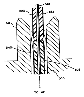
Figure 14 is a side elevational cross-section of an optical embodiment
according to the present invention.
CA 02330300 2000-10-26
WO 99/56352 PCT/US99/09163
11
--
Best Mode for Carrying Out the Invention
Referring first to the drawings, Figures 1 A and I B depict a high-density
electrical interconnect system 30 including a backpanel connector 40 and a
daughter card connector 35 according to the present invention. One side of the
backpanel connector 40 is mounted to a backpane142 and one side of the
daughter
card connector 35 is mounted to a daughter card (not shown) so that the
electrical
interconnect system 30 can be used to effect electrical interconnection of a
large
number of electrical signals between the backpanel 42 and the daughter card
when
the backpanel connector 40 and a daughter card connector 35 are mated
together.
As can be appreciated, the principles of the present invention can be applied
to
devices other tium daughter cards and backpanels and such are only used herein
for descriptive purposes. For example, instead of right angle connection
depicted
in Figure 1, the daughter card connector could be a straight connector. As
depicted, the invention is described with respect to a horizontal orientation
although the invention is usable in any orientation. As is later described,
the
backpanel connector 40 and the daughter card connector 35 each include
grounding means to avoid cross-talk between signals carried on adjacent pins
and
the introduction of other spurious signals into the signal path on either the
daughter card or the backpanel 42.
The backpanel 42 can be formed of a conventional multi-layer printed
circuit card having high-density electrical signal paths (not shown). The
backpanel connector 40 includes a body 44 having side walls 46, 47 and a base
48. A plurality of upstanding pillars 50 are formed in columns and rows in a 6
x 6
grid array for convenience. Any column and row grid pattern can be used. For
example, a 6 x 12, a 4 x 6 and 4 x 12 are contemplated. The 6 x 6 grid array
is
longer in the horizontal direction than in the height direction as depicted in
Figure
1. The sidewall 46 includes a longitudinally extending metallic plate 53
attached
to an outer surface of the sidewal146. The plate 53 is press-fit to the ground
plane
in the backpanel connector 40. Alternatively, the metallic plate 53 could be
CA 02330300 2000-10-26
WO 99/56352 PCT/US99/09163
12
formed by spraying an electrically conductive coating and then connecting same
-
to the ground plane in the backplane 42. The sidewall 46 is thus effectively
thicker than the sidewall 47 to provide polarity as discussed in detail below.
Although thirty-six pillars 50 are depicted, any number of pillars can be
used.
The backpanel connector 40 includes multiple projecting assemblies 49 which
include the pillar 50 and the signal contacts 52. Each of the projecting
assemblies
includes multiple sets 51 (Figure 2A) of projecting electrical signal contacts
52
arranged in sets of four around a central insulator pillar 50. The body 44
including side walls 46, 47 the base 48 and the central insulator pillars 50
is
preferably molded integrally from a thermoplastic polyester which is an
electrically non-conductive plastic material.
The electrical interconnect system of the present invention includes a
plurality of conductive contacts arranged in groups or sets, and each group is
arranged in a grid of groups of contacts to form a grid arrangement. Each
group
of conductive contacts may constitute the conductive section of a projection-
type
interconnect component that is configured for receipt within a corresponding
receiving-type interconnect component which includes a plurality of conductive
beams or, alternatively, each group of conductive contacts may constitute the
conductive section of a receiving-type interconnect component configured to
receive a corresponding projection-type interconnect component. The conductive
beams mate with the conductive posts when a projection-type interconnect
component is received within a corresponding receiving-type interconnect
component. The groups of contacts are arranged in rows and columns. For each
group of contacts, there is a set of four signal contacts and a central ground
contact. The projection type interconnect component (backpanel connector 40)
includes projecting type signal contacts and a receiving type ground contact.
The
receiving type interconnect component (daughter card connector 35) includes
receiving type signal contacts and a projection type ground contact.
CA 02330300 2000-10-26
WO 99/56352 PCT/US99/09163
13
The pillars 50 are each hollow and have a rectangular exterior with
surfaces 54, 56, 58, 60. For each pillar 50, a set of one of the four
projecting
signal contacts 52 abut the surfaces 54, 56, 58, 60, respectively. The
surfaces 54,
56, 58, 60 are each oriented at approximately 45 degrees relative to the
sidewalls
46, 47 as depicted in Figures lA and 1B. As depicted in Figure 2B, the
surfaces
54, 56, 58, 60 each include centrally located inwardly extending recesses 63,
64,
65, 66, respectively. Advantageously, the recesses 63, 64, 65, 66 are sized to
accept lateral edges of the signal contacts 52 to prevent lateral movement
thereof.
The projecting signal contacts 52 are electrically isolated from one another
by the
base 48 and the pillar 50. The projecting signal contacts 52 are inserted
through
the base 48 as described below. For each pillar 50, a central ground contact
62 is
positioned in the hollow pillar 50 and is electrically isolated from the
projecting
signal contacts 52 by the pillar 50.
The daughter card connector 35 includes a plurality of wafer assemblies
70 each connected to a hood enclosure 72. The hood enclosure 72 is made of
non-electrically conductive material such as thermoplastic polyester. As
depicted
in Figure 1B, there are six pairs of wafer assemblies 70 each having six sets
of
contacts 74 for a total of thirty-six sets of contacts corresponding to the
thirty-six
pillars 50. The wafer assemblies 70 are held together using an electrically
conductive stiffener 76 which is also connected to the hood enclosure 72. Each
set of contacts 74 includes four beam signal contacts 78. The beam signal
contacts 78 include beam sections for mating with the projecting signal
contacts
52 of the backpanel connector 40 as described in detail below. A central
ground
contact post 80 is positioned centeally between the four beam signal contacts
78
for mating with the central ground contact 62 in the backpanel connector 40.
In an alternative arrangement, either the central ground contact 62 or the
central ground contact post 80 can be omitted. Either the remaining ground
contact 62 or post 80 would then function as a ground shield. Spurious noise
and
signals would be carried by the contact 62 or post 80 to a respective ground
plane
CA 02330300 2000-10-26
WO 99/56352 PCT/US99/09163
14
in either the backplane 42 or daughter card. Also, alternatively the ground
contact
62 and the contact post 80 could be arranged so that the contact 62 and the
post 80
do not contact each other when the connectors 35, 40 are brought into the
mated
condition. In this manner, both the ground contact 62 and the contact post 80
function as ground shields.
Each of the wafer assemblies 70 comprises several electrically conductive
contacts 78 which include flexible beams 190. Preferably, the material of the
wafer is an insulative material thermoplastic polymer (Hoescht Celanese 3316).
Portions of the signal contacts 78 bend away from each other to receive the
projection-type interconnect component within the space between the flexible
beams.
Each signal contact 78 may be formed from the same materials used to
make the signal contacts 52 of the projection-type electrical interconnect
component. For example, each contact 78 may be formed of beryllium copper,
phosphor bronze, brass, or a copper alloy, and plated with tin, gold,
palladium, or
nickel at a selected portion of the conductive beam which will contact a
conductive post of the projection-type interconnect component when the
projection-type interconnect component is received within the receiving-type
interconnect component 35.
Alternatively, instead of contacts 78 and 52 carrying signals, these
contacts 52, 78 could be used as grounds and the contacts 62, 80 could carry
signals. This alternative arrangement has the disadvantage of carrying fewer
signals per square inch but the alternative arraiigement would approach the
performance of coaxial interconnect device. This alternative arrangement can
be
considered as psuedo-coax where each of the central signal carrying contact is
surrounded by four ground contacts. Because each of the signal carrying
contacts
is not surrounded by 360 degrees of ground, the arrangement is considered to
be
pseudo-coax. The center grounds 62, 80 could be replaced with optical
interconnect devices (Figure 14). Also the central contact could be replaced
by
CA 02330300 2000-10-26
WO 99/56352 PCT/US99/09163
shielded coaxial cable having a braid. The braid can act as a ground. The
center
post can be used to support an optical fiber which can be mated with a
corresponding optical fiber in the daughter card connector 35. The ends of the
optical fiber would be polished to optically transmit a signal.
5 Figure 2A is an enlarged view of a portion of the backpanel connector 40
depicting one pillar 50 and a set of the four signal contacts. In Figure 2A,
the
surfaces 54, 56, 58, 60 of pillar 50 are depicted having tapered upper
sections 82
to facilitate guiding the beam signal contacts 78 from the daughter card
connector
35 onto the projecting signal contacts 52. The projecting signal contacts 52
have
10 rounded upper sections 84 which further act to guide and effect a secure
mechanical and electrical contact between projecting signal contacts 52 in the
backpanel connector 40 and the beam signal contacts 78 in daughter card
connector 35 when the electrical interconnect system is mated. The ground post
62 is positioned in each pillar 50. The ground posts 62 may be commonly
15 connected to a ground plane within the backpane142.
Figure 2B depicts two pillars 50, 50a which are identical except for the
height of the pillars 50, signal contacts 52 and central ground contact 62.
The
different heights can provide for sequencing of contact. For example, the
taller
pillar and signal contacts 52 in the backplane connector 40 may contact the
contacts 78 in the daughter card connector 35 first.
Figure 2C illustrates that a pillar 50 can have signal contacts 52, 52b of
different heights. Sequencing may be achieved by varying the signal contact 52
height within the same pillar arrangement.
Referring now to Figure 3A, each projecting signal contact 52 includes
three contiguous sections: a contact portion 88, an intermediate portion 90,
and a
press-fit portion 92. In Figure 2, the contact portion 88 of each conductive
post is
shown in a position adjacent to and in contact with the pillar 70. The
intermediate
portion 90 is the portion of each projecting signal contact 52 that is secured
to the
base 48. The press fit portion 92 extends below the base 48 and into the
CA 02330300 2000-10-26
WO 99/56352 PCT/US99/09163
16
backpane142. As depicted in Figure 3B, a round press fit portion 94 extends
from
the intermediate portion 90 in a transverse direction for securing the
projecting
signal contact 52 to the base 48. The intermediate portion 90 has a lower
surface
96 to be brought into contact with a corresponding surface in the base 48. As
depicted in Figure 3B, the contact portion 88 has a flat surface 98 for
contact with
a corresponding surface 54-60 on the pillar 50. As depicted in Figure 3B, the
contact portion 88 of the projecting signal contact 52 includes a curved
contact
surface 100 having a peak 102, as depicted in Figure 3C. As depicted in Figure
3A, the press-fit portion 92 has two opposed spring like members 104 depicted
in
cross-section in Figure 3D. The press-fit portion 92 also has a lead-in
portion 106
at a distal end thereof.
The press-fit portion 92 shown is one type that may be used. Other press-
fit configurations may be substituted as required. Other termination methods
not
described here may be used if necessary, i.e., surface mount or through hole
solder type.
When the projection-type interconnect component 40 is received within a
corresponding receiving-type interconnect component 35, electrical signals may
be transferred from the press-fit portion 92 of each projecting signal contact
52
through the intermediate portion 90 and the contact portion 88 of projecting
signal
contact 52 to the receiving-type interconnect component (beam signal contact
78),
and vice versa.
Each projecting signal contact 52 may be formed of beryllium copper,
phosphor bronze, brass, a copper alloy, tin, gold, palladium, or any other
suitable
metal or conductive material. In a preferred embodiment, the projecting signal
contact 52 is formed of beryllium copper, phosphor bronze, brass, or a copper
alloy, and plated with tin, gold, palladium, nickel or a combination including
at
least two of tin, gold, palladium or nickel. The entire surface of each
projecting
signal contact 52 may be plated or just a selected portion corresponding to
the
portion of projecting signal contact 52 that will contact a beam signal
contact 78
CA 02330300 2000-10-26
WO 99/56352 PCT/US99/09163
17
when the projection-type interconnect component is received within the
corresponding receiving-type interconnect component.
The daughter card connector 35 includes thirty-six sets 74 of four beam
signal contacts 78. The beam signal contacts 78 may be arranged in groups of
four to electrically interconnect with projecting signal contacts 52 when
daughter
card connector 35 is mechanically connected with the backpanel connector 40.
The center of each group of signal contacts 78 includes the central ground
contact
post 80 which is received by ground contact 62 when the daughter card
connector
35 is mated with the backpanel connector 40.
Referring now to Figures 4A and 4B, the central ground contact 62 is
depicted having a pair of opposed flexible legs 110, 112 for mating with
central
ground contact post 80. The legs 110, 112 each have at their distal ends
curved
portions 114 for facilitating insertion of central ground contact post 80. The
central ground contact 62 is formed from a flat sheet of material and is
stamped
and flexible legs 110, 112 are twisted from an initially flat position 90
degrees to
oppose each other as depicted in Figure 4A.
At intermediate portions of the curved portions 114, the curved portions
114 extend toward each other and then away at the distal ends of the curved
portions 114. The central ground contact 62 has an intermediate portion 120
extending from the legs 110, 112. The central ground contact 62 is pressed
into
the base 48 through a hole 130 from the bottom side of the base 48 as
explained in
detail below. The central ground contact 62 is retained by an angled portion
132
spaced from a base portion 134. The angled portion 132 is spaced from the base
portion 134 a distance equal to the thickness of the base 48. The angled
portion
132 is sized and shaped to deflect the plastic material surrounding the hole
in the
base 48 so that the central ground contact 62 is permanently retained by the
base
48. The base portion 134 extends outwardly from the intermediate portion 120 a
further distance than the angled portion 132. A press-fit portion 136 extends
downwardly from the intermediate portion 120 so that the central ground
contact
CA 02330300 2000-10-26
WO 99/56352 PCTIUS99/09163
18
62 can be press-fit into the back plane 42. The press fit portion 136 can be
identical to the press fit portion 92 described previously. Alternatively,
other
electrical connection methods can be used.
The configuration of the press-fit portion 136 of each of the projecting
signal contacts 52 depends on the type of device with which that press-fit
portion
136 is interfacing. For example, instead of a press-fit portion, portion 136
can
have a rounded configuration if interfacing with a through-hole of a printed
wiring board. Other configurations may also be used. See for example the press-
fit pin disclosed in expired U.S. Patent No. 4,017,143, the teachings of which
are
hereby incorporated by reference in their entirety into the present
disclosure.
Figures 5A-5F depict the body 44 of the backpanel connector 40 without
either of the signal contacts 52 or the central ground contact 62 inserted
therein
for clarity. As depicted in Figure 5A, the holes 130 are located inside one of
the
corresponding pillars 50. Adjacent each of the pillars 50 are four slots 140
- through which signal contacts 52 are inserted. As depicted in Figure 5B, the
shoulders 142 are formed which extend inwardly from a lower surface 144 of the
base 48. As depicted in Figure 5C, the pillars 50 extend upwardly from an
upper
surface 146. As depicted in Figure 5D, the hole 130 is octagonal. As depicted
in
Figure 5E, a shoulder 146 is formed outwardly from the hole 130 . The ground
contact 62 is inserted into the hole 130 and the base portion 134 is brought
into
contact with the shoulder 146. The intermediate portion 90 is in contact with
the
shoulder 142.
The receiving-type electrical interconnect component of the present
invention includes several electrically conductive beams 190 (see Figure 6A)
preferably embedded in an insulative frame. The receiving-type electrical
interconnect component is configured to receive a corresponding projection-
type
electrical interconnect component within a space between the conductive beams.
The insulative frame insulates the conductive beams from one another so that a
different electrical signal may be transmitted on each beam.
CA 02330300 2000-10-26
WO 99/56352 PCT/US99/09163
19
Figure 6A illustrates a wafer assembly 70 attached to the stiffener 76 to --
form a portion of the receiving-type interconnection component 50 in
accordance
with an embodiment of the present invention. Each of the wafer assemblies 70
includes a right wafer assembly 162 and a left wafer assembly 164. As depicted
in Figure 6B, each set or group of the signal contacts 74 includes four signal
contacts 166, 168, 170 172 arranged at right angles to each around the central
ground contact post 80. As depicted in Figure 6A, signal contacts 166, 168 are
part of the right wafer assembly 162 and signal contacts 170, 172 are part of
the
left wafer assembly 164. As depicted in Figure 6A, all of the signal contacts
are
positioned at 45 degrees from vertical.
As depicted in Figure 6A, the wafer assembly 70 includes a right frame
180 and a left frame 182 which is injection molded around the plurality of
signal
contacts 78. Each of the frames includes a single column having six signal
contacts 78. Each of the signal contacts 78 is formed in a 90 degree arc and
is
formed such that contacts 78 have a flexible beam portion 190 extending from
front surfaces 240, 242 of the right frame 180 and the left frame 182. Each of
the
frames 180, 182 has a pie shape. Each signal contact 78 includes press-fit
portions 200, 202 which extend downwardly from frames 180, 182, respectively,
for electrical interconnection with a daughter card. The press-fit portions on
both
the daughter card connector 35 and the backpanel connector 40 advantageously
avoids soldering the connector to a circuit board. The press-fit connection
avoids
desoldering should the connector need to be repaired or removed from the
printed
circuit board which can be difficult because of the high density of the
electrical
interconnection system of the present invention. Alternatively, instead of
press-fit
portions 200, 202 other contact type portions or other portions can be used.
As
depicted in Figures 6A and 6B, the central ground contact post 80 is located
between a set of four conductive contacts 78. The wafer assemblies 180, 182
provide a right angle coiuiection between the daughter card and the backpanel
connector 42.
CA 02330300 2000-10-26
WO 99/56352 PCT/US99/09163
Figure 6A depicts that adjacent sets of signal contacts from the daughter
card may have ground pins 262 (ends not shown) interweaved therewith to reduce
cross-talk from signals carried on adjacent pairs of contacts 18. Needless to
say,
the contacts 78 and the ground pins 262 are formed and maintained to ensure
5 isolation between the signal carrying contacts 78 and the ground pins 262.
To
facilitate installation, either the signal contacts 78 or the ground pins 262
can have
insulated portions to reduce the possibility of electrical shorting between
the
central ground post 80 and the signal contacts 78. For example, portions of
each
signal contact can be formed with an insulated section, for example, by
spraying a
10 plastic insulation onto portions of the signal contacts to avoid having the
signal
pins from shorting out against the ground pins 262.
As depicted in Figure 7, a stamped frame 210 used in assembling the left
wafer assembly 164 is depicted in which adjacent signal contacts 78 are
connected by tabs 212. The interconnection of signal contacts using tabs 212
15 permits the stamped frame 210 to be placed in an insert reel-to-reel mold
and have
plastic embedded around the stamped frame 210. The tabs 212 are removed after
the insert injection molding process is completed.
Each of the frames 180, 182 each include a front frame portion 220, a
lower frame portion 222, a curved fr=une portion 224, and a left intermediate
20 frame portion 226 and a right intermediate frame portion 228. Because each
of
the frames is injection molded, frame portions 220-228 are integral with each
other. Front frame portion 220 is connected at a lower end thereof to a front
end
of the lower frame portion 222. The curved frame portion 224 is connected at
an
upper portion thereof to the front frame portion 222 and a lower portion
thereof to
the lower frame portion 222. The left and right intermediate frame members 226
and 228 extend from an upwardly extending portion 230 extending from the lower
frame portion 222 to intermediate portions of the curved frame member 224 to
form a hub and spoke.
CA 02330300 2000-10-26
WO 99/56352 PCT/US99/09163
21
The beam section 190 of the signal contact 78 is depicted in Figures 6C-
6F. With reference to Figure 6C, each flexible signal contact 78 includes the
beam
portion 190 which itself includes three sections: a contact portion 250, a
flexible
portion 252, and a stabilizing portion 254.
The contact portion 250 of each beam portion 190 contacts a conductive
signal contact 52 of a corresponding projection-type receiving component when
the projection-type receiving component is received within the corresponding
receiving-type interconnect component. The contact portion 250 of each beam
portion includes an interface portion 256 and a lead-in portion 258. The
interface
portion 256 is the portion of the beam portion 190 which contacts a tapered
upper
section 82 of the pillar 50 and the rounded upper section 84 of the signal
contact
52 when the projection-type and receiving-type interconnect components are
mated. The lead-in portion 258 comprises a curved surface which initiates
separation of the conductive beams during mating upon coming into contact with
the tapered upper surface 82 of the pillar 50 and the rounded upper surface 84
of
the signal contact 52.
Figures 8A-8D depict the left frame assembly 182. The right frame
assembly 180 is symmetrical to the left frame assembly 182 with the exception
of
a ground contact 300 which is included with one wafer and only a single ground
contact 300 per wafer assembly 70. A plurality of curved slots 270, 272, 274,
276, 278, 280 each extending in a 90 degree arc are spaced through left frame
182
for retaining the central ground contact posts 80. More specifically, there
are six
slots 270-280 which are formed in frame members 220, 226, 228 and 222 to shape
the central ground contacts 80 into a 90 arc. The curved slots 270-280 are
each
spaced from each other with each succeeding slot having a larger radius. The
central ground contact posts 80 (not shown in Figure 8) extend forwardly from
the
front frame portion 220 along with the beam portions 190 of each of the signal
contacts 78. The press-fit portions 202 extend downwardly from the lower frame
portion 222.
CA 02330300 2000-10-26
WO 99/56352 PCT/US99/09163
22
A plurality of pins 290, 292, 294 extend from the left frame 182.
Corresponding holes (not shown) are molded into right frame 180 so that the
frames 180 and 182 mate together to form a wafer assembly 70 after the ground
contact posts 80 are inserted between the left and right frames 180, 182. A
ground contact 300 is optionally embedded into the left frame 182 and has a
rearwardly extending portion 302 for contact with the electrically conductive
stiffener 76 and a forwardly extending portion 304 for contact with the
metallic
plate 53. The forwardly extending portion 304 is spring like and forms an
electrical connection against the metallic plate 53. Advantageously, the
ground
contact 300 provides a second grounding method preventing or reducing spurious
signals from affecting signals carried by the signal contacts 52, 78. If the
ground
contact 300 is omitted, then it is not necessary that the stiffener 76 be
electrically
conductive.
Referring to Figures 6 and 8A, the left wafer includes a tab 310 extending
upwardly and rearwardly from the intersection of the front frame portion 220
and
the curved frame portion 224 for insertion into a corresponding slot 320 in
the
stiffener 76. The slot 320 as depicted in Figure 9 includes a straight section
322
for receiving tab 200 and a pair of transverse receiving slots 324 for
receiving a
pair of tabs 326 which extend from an upper surface of the hood enclosure 72.
The hood enclosure 72 serves to locate and lock the wafer assemblies 70 in
position adding stability to the daughter card connector 35 after assembly to
the
stiffener 76. In addition, the hood enclosure provides alignment and
polarization
as discussed in detail below when the backplane connector 42 is being mated to
the daughter card connector 35.
In Figure 10, a snap receiving groove 330 is formed on the lower forward
surfaces of the right and left frames 180,182 for mating with a pair of
engaging
members 340 in the hood enclosure 72 as depicted in Figure 11.
In Figures 1 and 12A-12G a front protective member 400 is depicted for
protecting the beam portions 190 of the conductive contacts. The sets of
contacts
CA 02330300 2000-10-26
WO 99/56352 PCT/US99/09163
23
74 are vulnerable to damage without the front protective member 400. The front
-
protective member 400 has a plurality of openings 410 each for receiving a set
of
contacts 74. Surrounding each of the openings are extending portions 412 which
extend from a front surface of the front protective member 400 to close
proximity
of a front surface of the left and right frame members 180, 182.
In Figure 12E, the cover plate 400 is depicted in an exploded condition
and each of the signal contacts 78 is visible. In Figure 12F, the cover plate
400 is
depicted positioned within the hood enclosure 72. A distal end of the signal
contacts 78 is positioned inwardly from the cover plate 400. Advantageously,
the
cover plate 400 protects what might otherwise be vulnerable spring-like signal
contacts 78. The projecting pillars 50 and associated contacts 52 extend
through
the openings 410 to permit the contacts 52, 78, 62, 80 to make contact and
engage.
In Figure 12G, the cover plate 400 is illustrated as being aligned with the
hood enclosure 72 using a plurality of alignment tabs and slots including a
plurality of left alignment slots 420 and right alignment slots 430 formed in
the
cover plate which can be aligned with corresponding keys 440, 450 extending
inwardly from opposite sides of the hood enclosure 72. The cover plate can
only
be positioned in the hood enclosure in one orientation. Between upper 460 and
lower edges 462 of the cover plate 400 and an upper, inner surface 470 and a
lower inner surface 472 the hood enclosure 72 are formed two horizontal slots
having a first width and a second width. The wider slot can receive the wider
sidewall 46 and the narrow slot can receive the narrower sidewall 47.
Additionally, as depicted in Figure 12H, keys 480, 482 can be provided on the
body 44 to align with vertical slots 490, 492.
Figure 13 illustrates a projection-type interconnect component 40 received
within the conductive beams of a receiving-type interconnect component 35.
When the projection-type interconnect component is received within the
receiving-type interconnect component in this fashion, such interconnect
CA 02330300 2000-10-26
WO 99/56352 PCT/US99/09163
24
components are said to be mated or plugged together. When the projection-type -
-
and receiving-type interconnect components are mated, the flexible beam
portions
190 of the signal contacts 78 bend or spread apart to receive the projection-
type
interconnect component within the space between the contact portions of the
conductive beams.
The mated position shown in Figure 13 is achieved by moving the
projection-type interconnect component 40 and the receiving-type interconnect
component 30 toward one another. In the mated position, the contact portion of
each conductive beam exerts a normal force against a contact portion of a
corresponding one of the conductive posts.
The process of mating the backpanel connector 40 with a corresponding
daughter card connector 35 will now be discussed with reference to Figure 13.
The backpanel connector 40 and the daughter card connector 35 are moved
toward one another. Before the mating of the signal contacts 52, 78, the
central
ground post contact 80 spreads apart the legs 110, 112 of the central ground
contact 62. This preferably occurs before any contact occurs between the
signal
contacts 52, 78. Eventually, the contact portions 250 of each flexible signal
contact 78 contact the tapered upper sections 82 of the pillars 50 and then
the
rounded upper section of the signal contact 52. Upon further relative movement
of the interconnect components toward one another, the curved configuration of
the contact portion 250 causes the contact portions 250 of the flexible beams
190
to start to spread apart. Such spreading causes the flexible beams 190 to
exert a
normal force against the signal contacts 52 in the fully mated position,
thereby
ensuring reliable electrical contact between the signal contacts 52 and 78.
Relative lateral movement of the signal contacts 52 and 78 is prevented by the
rounded configuration of an intermediate portion of the signal contact and the
corresponding configuration of the interface portion 256 and lead-in portions
258.
With reference back to Figure 2B, it may be preferable to have different sets
of
contacts mate before other sets of contacts. Thus, pillar 50 height can be
adjusted.
CA 02330300 2000-10-26
WO 99/56352 PCT/US99/09163
For two different pillar 50 heights central ground contacts 62, 62a can
contact
simultaneously with posts 80, 80a and then signal contacts 52, 52a and 78, 78a
can be brought into contact. It should be understood that any sequencing can
be
attained to suit a particular application.
5 The insertion force required to mate the projection-type interconnect
within the receiving-type interconnect component is highest at the point
corresponding to the early phases of spreading of the flexible beams 190. The
subsequent insertion force is less as it relates to frictional forces rather
than
spreading forces. The insertion-force required to mate the projection-type and
10 receiving-type interconnect components can be reduced (and programmed
mating,
wherein one or more interconnections are completed before one or more other
interconnections, may be provided) using a projection-type interconnect
component having conductive posts which vary in height.
An alternative embodiment is depicted in Figure 14 where the central
15 ground contact 62 and the central ground contact post have been replaced
with an
optical fiber 500 and a fiber housing 502 and an optical fiber 510 and a fiber
housing 512, respectively. Surrounding the fiber housing 502 is an
electrically
conductive case 520. The optical fiber 510 and the electrically conductive
case
terminate to the daughter card (not shown). Surrounding the fiber housing 512
is
20 an electrically conductive case 530 and spring member 540. The optical
fiber 500
and the electrically conductive case 530 terminate to the backpanel 42. The
spring member 540 is annular and formed at the distal end of case 530 and is
coelctensive with case 520 to form an electrical contact to ground. The mating
ends of the optical fibers 500, 510 are polished optically flat as depicted in
Figure
25 14 for transmission of an optical signal. In all other respects, the
connector 30 is
the same as previously described.
It should now be apparent that an electrical interconnect system has been
described in which multiple grounding methods are used to ensure that spurious
signals and noise do not interfere with high speed transmissions. The
principles
CA 02330300 2000-10-26
WO 99/56352 PCT/US99/09163
26
of the present invention are particularly useful in high density electrical- --
connection systems which are susceptible to noise and interference .
It will be readily seen by one of ordinary skill in the art that the present
invention fulfills all of the objects set forth above. After reading the
foregoing
specification, one of ordinary skill will be able to affect various changes,
substitutions of equivalents and various other aspects of the invention as
broadly
disclosed herein. It is therefore intended that the protection granted hereon
be
limited only by the definition contained in the appended claims and
equivalents
thereof.