Note: Descriptions are shown in the official language in which they were submitted.
CA 02330433 2001-O1-09
1
Smart Exposure Determination for Imagers
Field of the Invention
The present invention relates to the field of image scanning devices and in
particular to scanning devices operating under a wide range of ambient light
intensity.
Background of the Invention
In the imaging industry, scanners are expected to operate effectively under a
wide range of ambient light. A number of solutions have been developed wherein
ambient light is measured in order to control the scanning system. The sensing
of
ambient light may be done by an ambient light detection circuit which is
separate
from the imaging array, or ambient light can be detected through the use of
the
imaging array itself . The ambient light measurement is then used either to
adjust the
exposure time of the imaging array/lens, to set the gain of the image signal
or to
control the brightness of a light source.
U. S. Patent 4,970,379 which issued on November 13, 1990 to Danstrom
discloses exposure/illumination control for a bar code scanner consisting of a
controllable light source and an optical sensor that is independent of the
scanner array.
The optical sensor converts the light reflecting from the object to be scanned
into an
electrical signal representative of the ambient light. This signal is coupled
to a
comparator which determines the illumination required by the scanner array and
then
adjusts the power to the controllable light source accordingly. A major
drawback of
this method is that during low light conditions the light source will be
driven by the
CA 02330433 2001-O1-09
2
comparator to generate bright illumination which consumes a large amount of
power.
In a hand held device this is extremely detrimental, as most hand held devices
have a
self contained power supply.
Other systems use the imaging array itself to determine ambient light levels
which is then used to control exposure time. U.S. Pat. 4,471,228 which issued
on
September 11, 1984 to Nishizawa et al describes an image sensor consisting of
non-
destructive readout-type image cells, the sensor uses the array of image cells
as both
photo-detector cells for the measurement of ambient light and as image
capturing cells
for imaging an object. The imaging array is exposed to the object and an
ambient
light measurement run is made through previously selected imaging cells. The
added
value of the selected imaging cells is compared to a reference value to
determine the
exposure level required. The selected imaging cells are then erased, and an
image
scan of the object is performed with a controlled exposure time.
The shortcoming of this method is that it consists of too many steps. The
process is slowed down by the multi-step process of using the array to measure
ambient light and then forcing the array to be reset before the image is
scanned.
Additionally, the extra step requires an extra expenditure of power, which is
a severe
detriment in a hand-held device.
U.S. Patent 4,338,514 which issued on July 6, 1982 to Bixby discloses a
further method of controlling exposure time by operating a mechanical shutter
in
response to radiant energy impinging on the sensor array. The semiconductor
array
substrate current is monitored during the exposure of the imaging array to
produce an
integrated signal that is proportional to the exposure level of the array. The
signal is
compared to a threshold voltage and when it exceeds a threshold value the
shutter is
closed.
CA 02330433 2001-O1-09
There are drawbacks to this method in that it requires additional processing
steps in order to create an apparatus to monitor the substrate current.
Specifically, the
apparatus requires the addition of a layer of conductive material between the
non-
conductive base-plate and the semi-conductive substrate. While this type of
process is
typical in some CCD imagers, it would be a costly addition in a CMOS imager.
A further system in which exposure time is adjusted is described in
U.S. Patent 5,986,705 which issued on November 16, 1999 to Shibuya et al. A
video
camera is described having an image sensing device, an exposure adjustment
apparatus which controls the gain of an amplifier to adjust the scanned output
signal
and further controls a drive pulse generator to control the exposure time of
sensing
device. In one embodiment, the video camera controls exposure by capturing an
image with the image sensing device, amplifying the output signal which is
driven
externally as well as being fed back into the exposure adjustment apparatus
where the
signal is compared to a reference. When the comparison indicates that the
image is
either overexposed, underexposed or without need of adjustment, control
signals are
sent to the drive pulse generator to adjust exposure time and to the amplifier
to adjust
the gain of the amplifier.
This method has several disadvantages, its iterative style of exposure control
is
only advantageous for a video camera. Controlling only exposure time and
signal
gain is limiting in terms of the range of light intensity under which the
device would
remain useful. Still cameras, bar code readers and the like, would not find
such a
method useful as it would require additional circuitry to filter out the
overexposed and
underexposed images. Low-light conditions would be difficult for the device to
image as it has no control over an external light source.
While each of the adjustment methods has its merits, the adjustment methods
are inherently limited by the range of light intensity in which they can
operate and in
the type of device to which they may be applied.
CA 02330433 2001-O1-09
4
Therefore, there is a need for scanning devices that can operate under a wide
range of ambient light intensity and maintain a high quality of image capture.
Summary of the Invention
S This invention is directed to a method and a system for maintaining the
output
signal of an imager at a predetermined operable level during the image capture
of an
object. This invention comprises sensing the intensity of the illumination on
the
object, storing a signal representative of the illumination intensity,
sampling the
representative signal and controlling the output signal as a function of the
sampled
representative signal.
In accordance with another aspect of the present invention, the output signal
may be controlled as a function of the sampled representative signal by
comparison to
a look-up table having a variety of control signal levels as a function of
light intensity,
exposure timing and amplifier gain.
With regard to a further aspect of this invention, the output signal may be
maintained by adjusting the exposure time of the imaging array, adjusting the
intensity of the illumination on the object and/or adjusting the amplification
of the
output signal.
In accordance with another aspect of this invention, the intensity of the
illumination on the object may be sensed from two or more sides of the imaging
array
by light detectors which are integrated on the imaging array die. These
detectors may
be used to repetitively sense the illumination on the object.
With respect to a further aspect of the present invention, the imager
comprises
a light source for illuminating the object to be imaged; the source may
include one or
more LED's positioned about the scanning array, preferably at the corners of
the
CA 02330433 2001-O1-09
array. The imager further includes light detectors which may include one or
more
photodiode/ integrator circuit combinations located along one or more sides of
the
imaging array.
S In accordance with a further aspect of this invention, alignment of the
imaging
array with the object may be determined by individually sensing the intensity
of the
illumination on the object from a number of position on at least two sides of
the
imaging array, comparing the signal representative of the illumination
intensity from
each of the positions to a signal representative of the outside edge of the
object, and
moving the imaging array over the object until the representative signals from
all of
the positions are substantially equal to the representative signal of the
outer edge of
the object as an indication of alignment. A further method of controlling
proper
image alignment comprises individually sensing the intensity of the
illumination on
the object from a number of position on at least two sides of the imaging
array,
comparing the signal representative of the illumination intensity from each of
the
positions to a signal representative of the outside edge of the object, and
isolating
portions of the imaging array that contains the object as a function of the
relative
signal levels. These alignment processes are particularly useful with image
recognition processes for imaged bar codes.
Other aspects and advantages of the invention, as well as the structure and
operation of various embodiments of the invention, will become apparent to
those
ordinarily skilled in the art upon review of the following description of the
invention
in conjunction with the accompanying drawings.
Brief Description of the Drawings
The invention will be described with reference to the accompanying drawings,
wherein:
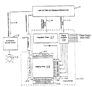
Figure 1 illustrates an embodiment of an imager with an imaging array and
light detection circuits in accordance with the present invention;
CA 02330433 2001-O1-09
6
Figure 2 illustrates an arrangement of light detection circuits about an
imaging
array;
Figure 3 illustrates a photodiode light detection circuit which may be used
with the present invention ;
Figure 4 is an arrangement of elements as seen from the scanner face;
Figure 5 is a block diagram of a further embodiment of an imager with an
image array and light detection circuits; and
Figure 6 is a block diagram of a controlled photodiode light detection
circuit.
Detailed Description of the Invention
CMOS image sensors are comprised of an array of light sensitive pixels
integrated on a die. After the pixels have been reset, the signal generated by
each
pixel is proportional to the amount of charge collected by the pixel during an
exposure
or integration period. The amount of light present when an image is being
captured
1 S by the image sensor can greatly influence the quality of the captured
image which is
particularly important when the captured image is being used for image
recognition in
instances such as for bar code reading. The amount of light present when an
image is
being captured may also influence the amount of amplification that the image
signals
require as they are being processed for image recognition.
Figure 1 illustrates the use of the present invention with a typical imaging
circuit 101 which is located on a wafer or die represented by broken lines.
The
imaging circuit 101 normally includes an imaging array 102, wordline drivers
103 and
wordlines 104, bitline readers 105 and bitlines 106, an integration timer 107,
and a
signal amplifier 108. The bitline readers 105 are connected to the signal
amplifier 108
which amplifies the bitline reader 105 signals to produce the image output
data.
Further in accordance with the present invention, light detector circuits 109
are also
located on the die 101 adjacent the imaging array 102. Though, the light
detector
circuits 109 are shown as being on two sides of the array 102, they may be
located on
all four sides of the array 102 as illustrated in figure 2, or even on one or
three sides of
the array.
CA 02330433 2001-O1-09
7
Figure 3 illustrates an example of a light detection circuit 109 that may be
used in accordance with the present invention. Light detection circuit 109
includes
one or more light detectors 301 each consisting of a p-n photodiode 302
(hereinafter
S referred to as a photodiode), an op-amp 303, a capacitor 304 and a reset
switch 305.
If a number of light detectors 301 are used in each light detection circuit
109, they
may be positioned in a row along the side of the imaging array 102. Generally,
the
control process for the light detectors 301 has the following steps. The reset
switches
305 are held closed until their corresponding photodiodes 302 are to be read.
The
photodiodes 302 may all be read simultaneously, however in the present
embodiment
the photodiodes 302 are sequentially read one at a time. When a photodiode 302
is to
be read the reset switch 305 is held open for a specified time so that the
charge related
to the ambient light can accumulate in the capacitor 304. The op-amp 303
integrates
the charge across the capacitor 304, which is coupled between its inverting
input
terminal 306 and its output 307. The non-inverting input terminal 308 is
connected to
a reference voltage.
The use of a p-n photodiode in the description of this embodiment is only
illustrative, any type of semiconductor light sensitive device could be used
in light
detectors 301, such as a p-i-n photodiode or a Schottky photodiode.
This process for detecting light level can be very rapid, thus allowing
several
cycles of light detection to be repeated during one cycle of image scanning by
the
imaging array 102.
Referring back to figure l, the imaging circuitry 101 on the die may further
include an averaging circuit 110, a look-up table and signal driver 111 and an
illumination source control 112. The signal driver 111 includes output lines
113 to
115 respectively for signals to control the signal amplifier 108, the
integration timer
CA 02330433 2001-O1-09
8
107 and the illumination source control 112. The illumination source control
112 is
adapted to control an light source 113 which itself would not be located on
the die. In
addition, components 110, 111 and 112 may not necessarily be located on the
imaging
circuitry die 101 as this will not affect the operation of the invention.
S
The operation of the imaging circuitry 101 follows. During the light detection
portion of the image acquisition cycle, the light detection circuits 109 are
allowed to
accumulate electric charge generated from the impact of light on their
photodiodes
302 or on other such light sensitive device. As the light detection circuit
109 is read,
the voltage is transferred to an averaging circuit 110 which produces a signal
or
plurality of signals representative of average ambient light; these signals
are
transferred to the look-up table and signal driver 111. The look-up table and
signal
driver 111 acts as a comparator, comparing the signals to an internal table of
values
for illumination, integration time, and signal gain corresponding to
particular ambient
light conditions.
The look-up table and signal driver comprises a microcontroller device such as
the Strong Arm SA1110, consisting of inputs for receiving information, outputs
for
driving external signals and a read-only memory. The read-only memory contains
a
software program that includes data relating to particular imaging needs in
terms of
light intensity, integration time and signal gain in response to a measured
level of
ambient light. The data mix contained therein would depend on the type of
application that the device is to be used; for example, a bar code reader
would rely
mostly on the adjustment of the integration time as this would be the power
conscious
method of acquiring a viable output signal.
Once the look-up table and the signal driver 111 determines the proper values
for the illumination source control signal, the integration time control
signal and the
gain control signal, these signals are fed to the illumination source control
112, the
integration timer 107 and the signal amplifier 108 to adjust the brightness of
the light
CA 02330433 2001-O1-09
9
source 113, the exposure time of the imaging array 102 and the gain of the
amplifier
108 respectively.
The light source 113 may consist of any type of conventional light source that
can be controlled in intensity. However, a particularly advantageous
arrangement is
illustrated in figure 4 which schematically illustrates the face of a scanner
401. The
imaging array 402 is located at the center of the scanner face 401, it has one
or more
light detectors 403 on one or more sides of the imaging array 402. In
addition, one or
more LED light sources 404 are positioned about the imaging array 402 to
provide
further lighting if required. In operation, the one or more LED's 404 may each
be
controlled by a separate line in order to turn each LED 404 OFF or ON as
desired.
For example, if an object or target is close to the scanner face 401, only one
or two
LED's might be turned ON; with the target a little further away, such as five
or six
inches, possibly three or four LED's 404 could be turned ON. Alternately, the
driving
current to each LED 404 could be controlled by the illumination source
controller 112
to increase or decrease the illumination from each LED 404 as required.
With reference to figure S, another embodiment of the invention using ambient
light detectors located on the same die as an imaging array will be described.
The
dual purpose of this embodiment is to measure ambient light conditions on an
object
being imaged and to align the imaging array with the object being imaged.
After the measurement of the appropriate exposure settings, as outlined in the
previous embodiment, the imaging array 502 must be aligned to the object to be
imaged, in the case of, for example, two-dimensional bar codes. This is
accomplished
by detecting the white space surrounding said bar code with the light
detection circuit
509 surrounding the imaging array 502. The detection circuit 509 includes a
plurality
of light detectors 511, each including a photodiode 512, a reset switch 515, a
capacitor
514 and an op-amp S 13 which operate similarly to the light detectors 301
described
with respect to figure 3.
CA 02330433 2001-O1-09
The ambient light detector control 503 is constructed to issue reset switch S
15
commands to each of the light detectors S 11. The light detectors S 11 are
held at reset
until a measurement of ambient light is required.
5 The ambient light detector control 503 allows the reading of individual
light
detectors 511 in sequence. In figure 5, light detectors S 11 are being read
starting at the
bottom left and proceeding upward and then to the right. In this particular
embodiment, there are 8 light detectors S 11 in a row to the left of the
imaging array
502 and 8 further light detectors S 11 in a row at the top of the imaging
array 502. For
10 simplicity, the light detectors 511 may be read in the order indicated
above, however
they may also be read in any order, as those skilled in the art will
recognize, the order
in which they are read can be varied significantly while yielding the same
result.
The averaging and image alignment circuit S 10 collects the data gathered from
the ambient light detectors 511, and performs two functions. The first is to
determine
alignment and the second is to average the light intensity signals. Alignment
may be
done by comparing the data to a value consistent with the background color.
The
comparison is repeated for the outputs of every light detector 511 until all
are found to
be consistent with the background color. This is achieved by moving and
adjusting
the scanner face 401 over the target. At this point, the averaging and image
alignment
circuit 510 outputs an image alignment indication signal to the image array
control
504 which indicates that the image is ready to be captured.
Alignment determination can also be performed in another way. The data can
be compared to a value consistent with the background color. The comparison is
repeated for the outputs of every light detector 511 until all have been
examined. This
data would then be communicated to a microcontroller for the purpose of
selecting
only a portion of interest from the object to be imaged. The microcontroller
then,
using this data relative to the positions of the detectors in relation to the
imaging array
CA 02330433 2001-O1-09
11
502, isolates the portions of the array 502 that can image the object of
interest. The
microcontroller then communicates to the imaging circuitry which portions of
the
array 502 to activate for the image acquisition cycle.
After these functions have been performed, the image array control 504 then
causes the imaging array 502 to capture an image of the object or target in
question.
The process by which the imaging array 502 captures an image is well known in
the
art and hence will not be explained further here. As with respect to the
system
described with respect to figure 1, the average ambient light signal 516 is
directed to a
look-up table and signal driver 111 which compares it to an internal table of
values for
illumination, integration time, and signal gain corresponding to particular
measured
ambient light conditions.
The look-up table and signal driver 111 determines the proper values for the
illumination source control signal, the integration time control signal and
the gain
control signal, and outputs those signals to the illumination source control
112, to the
integration timer 107 and to the signal amplifier 108 respectively which are
also
similar to those components as illustrated and described with respect to
figure 1.
An example of a controlled photodiode light detection circuit 600 of the type
which may be used in the system described with respect to figure 1 or 5 is
illustrated
in figure 6. The controlled photodiode light detection circuit 600 includes a
number
of light detection circuit 609 which as described with respect to figure 5 may
include
8 light detectors located in a row above the imaging array and 8 further light
detectors
located in a row along one side of the imaging array 502. Each light detector
comprises a photodiode and an integrator circuit.
The controlled photodiode light detection circuit 600 further includes a state
machine 602 which supervises the functionality of all of the blocks generating
logic
signals to control the timing of the controlled photodiode light detection
circuit 600.
A 16 channel analog multiplexer and sample/hold circuit 603 receives the
outputs of
CA 02330433 2001-O1-09
12
the 16 light detectors in the light detection circuit 609 and applies them to
a 5 bit
analog to digital converter 604 which consists of a comparator and a 5 bit
counter in a
typical single slope-A/D converter structure. A reference slope circuit 605
generates a
slope voltage that is selected by the state machine 602. Finally, the
controlled
photodiode light detection circuit 600 uses a data register 601 which
comprises an 8
bit write/read register and which is used as a buffer to a I2C Interface with
the look-up
table and signal driver 111.
By positioning the light detector circuits on the die adjacent to the imaging
array, and by providing the versatility of control of the light source, the
exposure
timing and/or the amplifier gain, the present invention provides a system
capable of
operating within a wide range of light intensities, from very low-light
conditions to
very bright conditions.
The present invention further has the advantage that it is able to measure the
ambient
lighting conditions from near the imaging array and has a low power
consumption.
The system in accordance with the present invention is further capable of
detecting
alignment of the image array with an object, thereby controlling the image
array to
produce an image that is conducive to image recognition.
In addition, since the light detectors are integrated on the same die as the
imaging array but function independently from the array, a signal
representative of the
ambient light at one location or another is always available for the control
of the light
source, the exposure time and or the amplifier gain at any time during the
image
scanning process. With light detectors located on opposite sides of the
imaging array,
ambient light can be detected for specific sides of the imaging array.
By using a number of LED's that can be controlled individually, substantial
power savings can be made by placing ON the minimum number of diodes required
and by varying the intensity of the LED's that are ON.
CA 02330433 2001-O1-09
13
While the invention has been described according to what is presently
considered to be the most practical and preferred embodiments, it must be
understood
that the invention is not limited to the disclosed embodiments. Those
ordinarily
skilled in the art will understand that various modifications and equivalent
structures
and functions may be made without departing from the spirit and scope of the
invention as defined in the claims. Therefore, the invention as defined in the
claims
must be accorded the broadest possible interpretation so as to encompass all
such
modifications and equivalent structures and functions.