Note: Descriptions are shown in the official language in which they were submitted.
CA 02330999 2000-11-O1
WO 99/66488 PCT/C1S99/11471
-1-
Description
CIRCUIT FOR TRANSFERRING HIGH VOLTAGE
VIDEO SIGNAL WITHOUT SIGNAL LOSS
TECHNICAL FIELD
The present invention generally relates to
video displays and more particularly such to displays
with capacitive elements and to circuitry for
transferring and storing high voltage video signals
without signal loss.
BACKGROUND ART
The pixels in a liquid crystal display
typically consist of a matrix of thin-film transistors
(TFTs) which are used to transfer a voltage to the liquid
crystal capacitor comprising each pixel of the display.
Gray scale imaging using liquid crystal displays
typically involve dividing each pixel into a plurality of
subunits. A desired gray level is obtained by activating
an appropriate number of such subunits. For example,
U.S. Patent No. 4,840,460 discloses a liquid crystal
display that is subdivided into a plurality of subpixels.
Each subpixel includes an effective capacitor, with the
liquid crystal material contained between the capacitor
plates. A control capacitor is coupled is coupled in
series with the effective capacitor. The capacitance of
the control capacitors can be controlled, thereby
activating the subpixels as a function of the applied
voltage across the series capacitance. Gray scale
imaging is achieved by activating an appropriate number
of subpixels for each pixel. U.S. Patent No. 5,576,858
teaches a similar structure of subpixels. These
approaches result in a complex pixel structure, and thus
increase the manufacturing difficulties in liquid crystal
panel fabrication.
A property of liquid crystal material is that
the transmissivity of the material to light is
CA 02330999 2000-11-O1
WO 99/66488 PCT/US99/11471
_2_
proportional to the voltage applied to the material.
While a high voltage level will cause the liquid crystal
material to become opaque, exposing the material to lower
voltages results in the attenuation of light passing
through the material. Thus, by storing an appropriate
charge at each pixel region in a liquid crystal layer
gray scale imaging can be obtained using a much simpler
structure than prior art approaches. However, a faithful
reproduction of an image requires accurate storage of
charge at each pixel.
Liquid crystal panels are commonly used in
computer display systems. The proliferation of laptop
units creates a demand for energy efficient displays,
owing to the fact that a laptop has a limited independent
source of power.
What is needed, therefore, is circuitry which
can transfer a video signal to a plurality of pixels
without degrading the quality of the signal. It is
desirable to provide circuitry which, for the most part,
operates at low voltage levels typical of CMOS devices,
but which can operate at the high voltage levels
typically encountered with the display of video signals
on a liquid crystal panel. It is further desirable that
low voltage operation be maintained whenever possible and
that high voltage operation is active only during the
creation of the image on the liquid crystal panel, thus
keeping to a minimum the power requirement of the liquid
crystal display.
SUMMARY OF THE INVENTION
In accordance with the present invention, a
video signal transfer circuit for transferring an analog
video signal from a video input node to a video output
node in response to receiving a select signal features a
pass transistor having a source-drain connection between
the video input node and the video output node; a second
transistor coupled to receive the select signal at a
first terminal thereof; a third transistor coupled to
CA 02330999 2000-11-O1
WO 99/66488 PCT/US99/11471
-3-
provide a voltage potential greater than the maximum
voltage level of the video signal to the gate of the pass
transistor in response to receiving a first logic level
at the second transistor; a fourth transistor coupled to
turn off the third transistor in response to receiving a
second logic level at the second transistor; and a fifth
transistor coupled to provide ground potential to the
gate of the pass transistor in response to receiving the
second logic level at the second transistor.
Further in accordance with the present
invention, a video display circuit for receiving and
displaying an analog video signal includes at least one
video signal storage element, a first transistor coupled
to receive the video signal and to pass the signal to the
storage element. A first drive circuit biases the first
transistor in a manner that the video signal is passed,
unattenuated, in response to receiving a first select
signal. A second transistor is coupled to a video source
and passes a received video signal to the first
transistor, unattenuated, in response to receiving a
second select signal.
BRIEF DESCRIPTION OF THE DRAWINGS
Figs. lA and 1B show a video display chip in
accordance with the invention.
Fig. 2 illustrates the signal flow owing to the
circuitry of the present invention.
Figs. 3A and 3B show the driver circuits of the
invention.
BEST MODE FOR CARRYING OUT THE INVENTION
A video display chip 100 in accordance with the
present invention comprises an array 102 of video storage
elements 20, as shown in Fig. lA. A liquid crystal layer
formed atop the array of storage elements responds
locally to the presence of a charge stored in a storage
element 20. The liquid crystal layer is separated from
storage elements 20 by an insulative layer (not shown).
CA 02330999 2000-11-O1
WO 99/bb488 PCT/US99/11471
-4-
Consequently, the area of the liquid crystal layer above
each storage element is capacitively coupled to it.
These areas in the liquid crystal layer are represented
schematically by capacitor elements 22. Typically, the
liquid crystal layer is coupled to ground potential.
This is shown schematically by a conductive line 106
representing a ground plane where XBIAS is ground. The
electric field from the charge stored in a storage
element 20 and its corresponding capacitive element 22
affects the transmissivity of light through the liquid
crystal layer; a greater stored charge, and hence a
greater resulting electric field, causes the liquid
crystal to become more opaque.
Continuing, a column selector 110 outputs logic
signals via a plurality of column select lines 118 to
provide column addressing of the array. Column select
lines 118 feed into column driver circuitry 116, each of
which has an output that controls the gate of a column
pass transistor 114. Similarly, a row selector 120
outputs logic signals via a plurality of row select lines
128 to provide row addressing of the array. Row select
lines 128 feed into a plurality of row driver circuitry
126, each of which has an output that controls the gate
of a row pass transistor 124. Thus, each video storage
element 20 is individually addressed by proper selection
of a column select line and a row select line. In the
preferred embodiment of the invention, column selector
110 and row selector 120 are CMOS devices powered by
V[~~], which for CMOS devices is typically a 5V power
rail. Consequently, the column and row logic signals
vary between one of two voltage levels, namely Ov and 5V.
A video signal source 10 provides the video
signal to be stored in video storage elements 20. The
video signal is a continuous analog signal having a
signal range between OV and 16V. A video signal line 12
is coupled via pass transistors 114 to deliver the video
signal to column lines 112. Column lines 112, in turn,
are coupled to storage elements 20 via pass transistors
CA 02330999 2000-11-O1
WO 99/66488 PCT/US99/11471
-5-
124 so as to deliver the video signal to individually
selected storage elements.
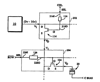
Referring now to Fig. 2, a selected column and
row define video signal transfer circuitry 202 and 204,
respectively, which cooperate to transfer the analog
video signal to a target video storage element 20. Each
video signal transfer circuit includes a select input
SEL, a video signal input VI, and a video signal output
VO. Video signal transfer circuit 202 comprises column
driver circuit 116 and column select transistor 114.
Column select line 118 is coupled to select input SEL
which feeds into an input 216I of driver circuit 116. An
output 2160 of driver circuit 116 feeds into the gate G
of transistor 114. Video signal line 12 is coupled to
video input VI which feeds into the drain terminal D of
transistor 114, passing the video signal to its source
terminal S as video output VO and onto column line 112.
Video signal transfer circuit 204 comprises row
driver circuit 126 and row select transistor 124. Row
select line 128 is coupled to select input SEL which
feeds into an input 226I of driver circuit 126. An
output 2260 of driver circuit 126 feeds into the gate G
of transistor 124. Column line 112 is coupled to video
input VI which feeds into the drain terminal D of
transistor 124, passing the video signal to its source
terminal S as video output VO and into storage element
20, which in the preferred embodiment is a capacitive
element.
Turn for a moment to Figs. lA and 1B. Video
source 10 of the embodiment shown in Fig. lA provides a
single video signal line 12 which feeds into each column
of array 102. Thus, storage elements 20 are loaded with
a video image in sequential order, each element being
addressed and charged up with the appropriate charge from
video signal line 12. Alternatively, video source 10 can
be designed to provide two or more video signal lines as
shown by video signal lines 12A and 12B in Fig. 1B. In
this embodiment, array 102 is divided into side 1 and
CA 02330999 2000-11-O1
WO 99/66488 PCT/US99/11471
-6-
side 2. Video signal line 12A feeds the column lines 112
belonging to side 1 and video signal line 12B feeds the
column lines 112 of side 2. This embodiment has the
advantage of allowing for a faster loading of a video
image by splitting the image into two halves and loading
each half simultaneously, albeit at the expense of
additional circuitry for proper synchronization of the
split image.
With reference to Figs. 3A and 3B, shown are
the column and row driver circuits 116 and 126
respectively the video signal transfer circuitry 202 and
204. Column driver circuit 116 comprises an input
terminal 216I that is coupled to a first terminal 302A of
N-channel MOS transistor 302. A second terminal 302B is
coupled to a node 392. The gate terminal 3026 is coupled
to V~~, typically a 5V power rail as mentioned above. A
P-channel MOS transistor 308 has a gate terminal coupled
to node 392, a source terminal coupled to Vh, and a drain
terminal coupled to a node 394. In accordance with the
invention, Vh is greater than the maximum voltage level of
the video signal, namely 16V. In the preferred
embodiment of the invention, V,, is an 18V power rail. A
second P-channel MOS transistor 306 has a gate terminal
coupled to node 394, a source terminal coupled to Vh, and
a drain terminal coupled to node 392. A second N-channel
transistor 304 has a gate terminal coupled to node 392, a
source terminal to ground, and a drain terminal coupled
to node 394. Finally, node 394 is coupled to output
terminal 2160 of video signal transfer circuit 116.
With reference to Fig. 3B, row driver circuit
126 comprises an input terminal 216I' that is coupled to
a first terminal 302A' of N-channel MOS transistor 302'.
A second terminal 302B' is coupled to a node 392'. The
gate terminal 302G' is coupled to V~~. A P-channel MOS
transistor 308' has a gate terminal coupled to node 392',
a source terminal coupled to Vh, and a drain terminal
coupled to a node 394' A second P-channel MOS
transistor 306' has a gate terminal coupled to node 394',
CA 02330999 2000-11-O1
WO 99/66488 PCT/US99/11471
a source terminal coupled to Vh, and a drain terminal
coupled to node 392'. A second N-channel transistor 304'
has a gate terminal coupled to node 392', a source
terminal to ground, and a drain terminal coupled to node
394'. Node 394' is coupled to the gate terminals of a
third P-channel transistor 310 and a third N-channel
transistor 312. Third transistors 310 and 312 have a
common drain connection, which in turn is coupled to
output terminal 2260 of video signal transfer circuit
126. The source terminal of third PMOS transistor 310 is
coupled to V," while the source terminal of third NMOS
transistor 312 is coupled to ground.
Operation of the video signal transfer
circuitry will now be discussed with reference to the
Figs. 2 and 3A. Consider first, video transfer circuit
202 shown in Fig. 2 and the associated driver circuit 116
shown in Fig. 3A. The voltage appearing at input
terminal 2161 is going to be either OV or 5V, recalling
that the column select signal is either OV or 5V (V
Consider the first case where column selector 110 outputs
a column select signal at a first logic level, feeding OV
into input terminal 216I. Since transistor 302 is always
ON by virtue of its gate being coupled to V~~, node 392
will also be at OV. This has the effect putting
transistor 304 in a non-conducting state. However,
transistor 308, a P-channel device, becomes conductive,
bringing node 394 to a potential equal to Vh. In
addition, transistor 306 is put in a non-conductive state
by virtue of the high potential (V,,) at node 394.
Continuing with Fig. 2, the gate terminal of transistor
114, being coupled to node 394, is biased at Vh thus
turning ON the transistor.
Recall that a transistor is conductive so long
as the gate-to-source voltage is greater than the
threshold voltage Vt,, of the transistor. Since the gate
of transistor 114 is biased at Vh, the source terminal of
conducting transistor 114 can rise to a voltage level
equal to Vh - Vth. Since Vh is 18V and Vth is typically
CA 02330999 2000-11-O1
WO 99/66488 PCT/US99/11471
_g_
0.7V, the source terminal of pass transistor 114 can rise
to a potential roughly equal to 17.3V. Since the video
signal has a maximum voltage level of 16V, the drain
terminal will see a maximum voltage level of 16V which
can be transferred to the source terminal, leaving
approximately a 1.3V margin for error. Thus, video
transfer circuit 202 is capable of selectively
transferring a video signal from its video input line VI
to its video output line VO without any degradation to
the video signal.
Consider next the case where column selector
110 outputs a column select signal at a second logic
level, feeding a 5V potential into input terminal 216I
switches to 5V. Node 392 will rise to approximately
4.3V, assuming Vth of transistor 302 is 0.7V. This will
have the effect of turning ON transistor 304 which will
take node 394 to ground potential. This in turn will
turn OFF pass transistor 114, thus preventing the
transfer of the video signal from video input line VI to
video output line VO.
Notice, however, that transistor 308 remains in
the conductive state despite the 4V bias on its gate
terminal, and thus burns power by virtue of the ground
path through transistor 304. The reason transistor 308
remains ON is that its V9a remains greater than its Vtn,
recalling that transistor 308 is P-channel and Vg is at 4V
and Vg is at Vh = 18V. In order to turn OFF transistor
308, its gate potential must be raised to a potential
greater than V,, - Vth. Transistor 306 provides the needed
potential. Since node 394 is at ground potential,
transistor 306 becomes conductive and its drain terminal
begins to rise to a potential of Vh. This will take the
gate terminal of transistor 308 to a potential sufficient
to turn it OFF.
Since the drain of transistor 306 is coupled to
node 392, the potential at node 392 will also rise to Vh.
This high potential would be damaging if it passed back
to the circuitry of column selector 110. Transistor 302,
CA 02330999 2000-11-O1
WO 99/66488 PCT/US99/11471
-9-
however, serves to block Vh. The potential at terminal
302A is 5V and the potential a terminal 3028 is at Vh, and
since transistor 302 is an N-channel device, terminal
302A acts as the source and terminal 3028 serves as the
drain. As such, transistor 302 becomes non-conducting
when V,, appears at node 392 because V9g is less than the
transistor's Vt,,. The effect is that the high potential
at node 392 does not pass back into the circuitry
comprising column selector 110, being blocked by
transistor 302.
Referring now to Figs. 2 and 3B, it can be seen
that operation of video signal transfer circuit 204 in
connection with the row select signal is virtually
identical to the foregoing discussion in connection with
transfer circuit 202. Drive circuit 126, however,
includes two additional transistors 310 and 312. In
accordance with the preferred embodiment of the present
invention, the row select signal is active LOW, as
indicated in Fig. 2. Transistors 310 and 312 therefore
are configured as an inverter to reverse the polarity of
the control signal that feeds into the gate terminal of
pass transistor 124. Note that the inverter circuit is
powered by Vh. This is to ensure that the HIGH output of
the inverter circuit is at V,, in order to properly bias
the gate terminal of pass transistor 124 for the reason
as discussed in connection with pass transistor 114.
In summary, video signal transfer circuit 202
transfers the analog video signal appearing at video
input line VI to video output line VO when a OV logic
level is presented at select line SEL. Conversely,
transfer circuit 202 blocks the video signal from video
output line VO when a 5V logic level is presented.
Similarly, video signal transfer circuit 204 passes the
video signal when the row select signal is at a logic
level of 5V and blocks the video signal for a logic level
of OV. Thus, by appropriately setting the column and row
select signals, the video signal can be transferred to
any of the storage elements 20.
CA 02330999 2000-11-O1
WO 99/66488 PCT/US99/11471
-10-
The video transfer circuits 202 and 204 permit
the use of a low power source (V~~) to power most of the
systems of the video display chip, while at the same time
providing unattenuated transfer of high voltage video
signals. By limiting the use of V,, only to the transfer
circuitry, the power requirements of the display chip are
kept to a minimum.