Note: Descriptions are shown in the official language in which they were submitted.
CA 02331430 2001-01-18
1
I)ernodulation structure and method
Fielci of the Invention
The present invention relates to a ciemodulation strueture anci a method for
downconverting and demodulating a modulated digital signal.
Back,iround of'the Invention
Demodulation structures ancl methods for downconvertina and demodulating a
di,,itally
modulated signal are known from and uscd in many ditferent applications, in
which
si27nals are transmitted from a transmitting apparatus to a receiving
apparatus. Thc
transmission can be eit~ier wireless over an air intertace or through a wired
connection.
Or` course, the chosen structtire and method for downconvertina and
demodulatin~~, a
transmitted digitally modulated sigral depends essentially on the moclulatiol
sch:,,mc
used on the transmitting sicle and the transmission medium.
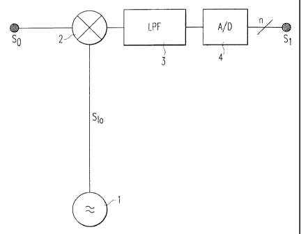
Figure 10 shows an example for a demodulation strueture for downconverting and
demodulating a dibitally modulated si~nal St). The shown demodulation
structure is
e.-. used for downconverting and demodulating a high frequency signal (RF
signal)
receiveci in a mobile terminal of a wireless telecommunication systern, such
as the GS NI
or the UNITS systein. Hereby, a transmitted RF signal is received by an
anterina of the
mobile terminal and supplied to a KF receiver. The diQital RF sianal is then
supplied to
a demociulation structure as e.g. shown in fi(yure 10. Another possibility
could be to
downconvert the RF sil-nal into an intermediate frequency band, whereatter the
intermediate signal is further downconverted and demodulated in a structure as
shown
in tivure 10.
In wireless telecommunication, usually <in I/Q-modulation is used, :n which
the
modulation states can be represented in an I/Q-diaaram. The horizontal axis
herebv
represents the I part, i.e. the part of the signal component which is in phase
to the
carrier si-nal, and the vertical axis represents the Q part, i.e. the
quadrature component
perpendicular to the phase of thc carrier signal. The digitat informatioil
signat is ':hus
transmitted by means ot the phase of the carrier signal, whereby the phasc of
tlle carrier
signal is switched bttw,cen the ditterent cliscrete states depenctinl- on tl,e
symbol to be
transmitted. Ttlis so-called phase shift key modulation (PSK modulation) is
used in
rnany ciifferent application areas, very otteri in combination with amplitude
shitt keyi:h-Y.
'1'he GSNI e.g. uses a GNISK modulation (Gaussian rninimum shift keying
mo(lulation).
CA 02331430 2008-03-06
2
Demodulation and downconversion of correspondingly I/Q-modulated signals is e.
g.
done by analog demodulation structures as shown in figure 10 comprising a
local
oscillator 101, two mixers 102, 103, a 90 degree phase shifter 104, two
lowpass filters
105, 106 and two analog-to-digital-converters 107, 108. A local oscillator
signal
generated in the local oscillator 101 is directly supplied to the first mixer
102 and
indirectly supplied to the second mixer 103 via the 90 degree phase shifter
104. In the
mixers 102 and 103, the digitally modulated signal So is mixed with the
corresponding
local oscillator signal and the phase shifter local oscillator signal,
respectively, so that
two separate output streams, one for the in phase (I) part and one for the
quadrature
phase (Q) part are generated. After further processing in the lowpass filters
105 and 106
and the analog-to-digital converters 107 and 108, the in phase part and the
quadrature
phase part are obtained in parallel as digital signals SI and SQ.
The disadvantages of this conventional approach are that the necessary 90
degrees phase
shifter is an analog device which is inherently frequency dependent and thus
limiting the
frequency range of the entire demodulation structure due to the increasing
phase and
amplitude imbalances. Further, since two parallel output streams are
generated, two
mixers, two lowpass filters and two A/D-converters are required, so that the
entire
demodulating structure requires many parts and becomes therefore expensive.
Summary of the Invention
The object of the present invention is therefore to provide a demodulation
structure and
a method for downconverting and demodulating a digitally modulated signal,
which is
simple in construction but still effective in operation.
This object is achieved by a demodulation structure for downconverting and
demodulating a digitally modulated signal, with a local oscillator
means for providing a local oscillator signal, a mixer means for mixing said
local
oscillator signal and said digitally modulated signal in order to obtain a
mixed signal, a
lowpass filter means for lowpass filtering said mixer signal from said mixer
means, and
an analog-to-digital converting means for converting the filtered signal from
said
lowpass filter means into a downconverted and demodulated digital signal,
whereby said
local oscillator signal is set in respect to said modulated digital signal so
that said
downconverted and demodulated digital signal output from said analog-to-
digital
converting means comprises two serially arranged information parts.
Compared to the state of the art, the demodulation structure and method are
particularly
advantageous since the two information parts are obtained serially instead of
parallel
CA 02331430 2001-01-18
}
which allows a very simple construction of the respective devices. This is
particularly
advantageous in case of an application of the present invention in mobile or
portable
terminals, like mobile terminals for a wireless telecommunication system,
since the
overall weight can be significantly reduced. Further, the usually analog phase
shifters of
the prior art devices can be omitted and therefore the amplitude and the phase
iinbalances can be essentially reduced. Further, the present invention has the
potential
to provide demodulation structures and methods with a larger bandwidth of
operation as
the prior art.
Advantageously, the digitally modulated signal is I/Q-modulated and the two
serially
arranged inforrnation parts comprised in the downconverted and demodulated
digital
signal are an I-part and a Q-part of the I/Q-modulated digital signal.
Further advantageously, the digitally modulated signal is modulated in a
signal band
having a center frequency and said local oscillator signal has a center
frequency, which
is, in respect to the center frequency of the signal band, offset by half of
the signal
bandwidth of the modulated digital signal.
Alternatively, the local oscillator signal is modulated with at least two
modulation states
having different phases during the synlbol period of the digitally modulated
signal. In
this case, the two different modulation states may have the same magnitude and
a 90
degree phase shift in respect to each other. The demodulation structure
according to the
present alternative of the present invention may further comprise a modulation
control
means for supplying a modulation signal to the local oscillator means in order
to
internally modulate the local oscillator signal with the two modulatiori
states.
Alternatively, the demodulation structure of the present alternative of the
clemodulation
structure according to the present invention may comprise an analog circuit
means for
nlodulating the local oscillator signal from the local oscillator means with
the two
modulation states and outputting a modulated local oscillator signal to the
mixer means.
Hereby, the analog circuit means may comprise a switch means which can be
switched
between a first branch having a phase shift means and a second branch having
no phase
shift means, whereby the switch means is switched by means of a control signal
with a
frequency of at least two times ttle symbol fl-equency of the digitally
modulated signal.
The present alternative of the demodulation structure according to the present
invention
may further advantageously comprise a bandpass tilter for bandpass tiltering
the
modulated local oscillator signal. Advantageously, the bandpass filtcr has a
center
frequency corresponding to the center frequency and a bandwidth corresponding
to the
bandwidth of the sianal band of the digitally niodtilated signal.
CA 02331430 2008-03-06
4
Brief Description of the Drawings
In the following description, the present invention is explained in more
detail in relation
to the enclosed drawings, in which
figure 1 shows a schematic block diagram of a first embodiment of a
demodulation structure according to the present invention,
figure 2 shows the block diagram of figure 1 with additional representations
of
center frequencies and frequency bands of the signals in the different parts
of the
demodulation structure,
figure 3 shows a simulation result for I/Q-values obtained for the modulation
structure as shown in figure 1,
figure 4 shows a schematic block diagram of a second embodiment of a
demodulation structure according to the present invention,
figure 5 shows a schematic block diagram of a third embodiment of a
demodulation structure according to the present invention,
figure 6 shows a more detailed representation of an analog circuit means
comprised in the demodulation structure shown in figure 5,
figure 7 shows a simulation result for I/Q-values obtained for a demodulation
structure as shown in figure 4 or 5,
figure 8 shows a schematic representation of center frequencies and frequency
bands for a demodulation structure as shown in figure 1 in a multichannel
environment,
figure 9 shows a schematic representation of center frequencies and frequency
bands for a demodulation structure as shown in figures 4 or 5 in a
multichannel
environment, and
CA 02331430 2001-01-18
J
tigure 10 shows a scheinatic block dia,gram of a demodl_iiation structure
accorcfing to the prior art.
Detailed Description ol'thc Pi-efei-red Enibokliments
The following description relates to the downconversion and demodulation of an
IiQ-
modulated signal. However, it is to be unc'erstood that the demodulation
structures and
methods shown in ancf explained in relation to the enclosed fiQures mav be
applied to
the downconversion and demodulation of other digitally modulated signals.
Figure 1 shows a schematic block diagram of a lirst embociiment of a
der:iodulation
structure tor downconverting and demodulatinQ an 1/Q-rnodulated signal S,,.
The I/Q-
modulated siLnal S,, may e.g. be supplied from a HF part of a receivino
device, C.g.
comprise(i in a mobile terminal or a base station of a wireless
telecommunication
system. The demodulation structure shown in fi-ure 1 comprises a local
oscillator
means 1 for generatinn a local oscillator si, nal S,,,. The local oscillator
si nal provided
from the local oscillator means 1 has a center frequency f, which, in respect
to the
center frequency f~ of the I/Q-modulated sigyna[ S, in the respective Signal
band, is
offset by half of the Signal bandwidth of the I/Q-modulated sil-nal S,'). Sõ
is e.g. pa:t ot
a high frequency band or an intermediate frequency band dependinc', if a
received high
frequency Signal is downconverted before being supplied to the demodulatiorl
structtire
shown in figure 1 or not.
Schematic representations of the frequency bands and center frequencies of the
[/Q-
modulated signal S, and the local oscillator signal S,. are shown i.n [igure
2. .Assuming
that the I/Q-modulated signal Sõ has a signal bandwidth B and a center
trequericy t_, the
center frequency t, of the local oscillator siLnal S,,, may e.,'. be locatcd
on the upper
end of the signal band of the I/Q-111odulated signal S,,, so that the cente.r
frequency f, ot
the local oscillator signal S,,, is equal to f_4-B/2. Alternatively, the
center frequency f,,,
of the local oscillator si-nal S,,, may be located at the lower edge of the
signal band of
the I/Q-modulated sional S,,(f,,,=fc-B/2).
The local oscillator signal S,~ and the I/Q-modulated signal So are mixed in a
single
mixer means 2 in order to obtain a mixed signal, which is lowpass liltered in
a lowpass
lilter ineans 3 so that a baseband signal with a cutoff frequency B
corresponding to the
sional bandwidth of the I/Q-modulatcd sigrial S,, is obtained. The hltercd
signal output
from the lowpass tilter means 3 is supplied to an analog-to-digital converter
4 tor an
analog-to-di'aital conversion at a sampling rate of twice the symbol rate of
the IiQ-
modulated sibnal S,,. In other words, the sampling is performed twice per
symbol len-th
of the 1;Q-modulated signal S,,. However, a tlip in the si,_,n of the samplud
1- and
CA 02331430 2001-01-18
0
Q-values from clock cycle to clock cycle occurs so that some further
processing- in this
respect is required.
Considering the case that the local oscillator signal S,o has a centel-
freqtiency of
f,o=f,+B/2, the operation of the demodulation structure shown in figure 1 anci
tigure 2
is explained. The I/Q-modulated signal S, can be represented by:
s(t)=i(t)cos(w,t)+q(t)sin(ca,t)
whereby w,=2;zf, ancl i(t) and q(t) are a baseband I signal and Q signal,
respectively.
They should be filtered such that symbol interference is avoidecl. In the
mixer me.ans 2,
the I/Q-modulated signal S, is multiplied with the local oscillator signal S,,
having a
center frequency f,,=f,-f-B/2, so that the followin(Dr mixed signal is
obtained:
s'(t)=sJt)*sõ(t)= acos((co,+TcB)t)*sjt)
= a i(t)cos(((~,+,7B)t)cos(co,t)+ a q(t)cos((o,+7iB)t)sin(o,t)
u a
_ 2 -i(t)[cos(,j7Bt)+cos((2(o,+TcB)t)]+ 2 q(t)[sin(,-rBt)+sin((2(0,+,-CB)t)]
After filtering out the higher frequency component in the lowpass filter
mearis 3, the
low frequency component is obtairied:
a a
s(t) ~ i(t)cos(~Bt)+ ~ q(t)sin(rrBt)
By sampling at discrete points in time at t=n/2B, either the cosinus or the
sinus
function is zero, so that i(n/2B) and q(n/2B) can be extracted at either
sainple. Since the
sampling rate f, is twice the synibol rate (fd=2B), the lowpass filter means 3
must have
a corner or a cutoff frequency of at least B. The signal output from the
anal.og-to-digital
converter means 4(signal S,) then serially comprises the I part and the. Q
part within
each symbol period of the I/Q-modulated signal.
In figure 3 the signals versus time are depicted in a simulation result. Here,
the clock is
indicated by hairlines and the original I (dashed) and Q(dash-dotted) signals
are also
shown as ideal rectangular signals in parallel. At last, the demodulateci
analoo signal
(thick line) is shown, where I and Q at different halves of each clock cycle
inciicate
whether the I or the Q signal can be picked up at this time. The ad(litional
sign " - "
indicates a flip in the sign of the value due to the theory of operation. As
an example
the tirst two clock cyclk~s are considered. In the first half the value of the
downconvertcd signal is high lcading to a"1" fOr the I-value. In the ')Ccund
half the
CA 02331430 2001-01-18
value is still high, but due to an a-priory known change in the sign we yielcl
"-1" as the
Q-value. Third half: analog value high, which equals "-1" for I(because of
minus si"'n)
and at last again "-1 " for Q (low analog value, no minus sign) and so forth.
"_Chus, we
obtain the serial sequence 1-1-1-1... or as usual I=1-1... and Q=-1-1...in
parallel. For
simplicity in this example we have only used QPSK modulation, but hi-her order
modulation schemes should equally be possible. The correct analog I- anci Q-
values or
parts serially comprised in the output signal S, are available at the
timepoints
(1/4+n/2)*Tg, whereby n is the sarnple number and T,=1/2B, so that the I part
is
obtained for even n and the Q part is obtained for odd n.
Figure 4 shows a schematic block diagram of a second embodiment of a
demodulation
structure aecording to the present invention. The entire structure comprises a
local
oscillator means 5 generating and outputting a local oscillator signal S,,
which is
modulated by means of a modulation signal generated and output by a modulation
control means 7. The local oscillator signal S,o is modulated witl, at least
two
modulation states with clifferent phases. Preferably, the second modulation
state has the
same magnitude and the 90 degree phase shift in relation to the first
modulation state,
whereby the modulation states are changing alternatively, as e.g. 010101...,
whereby at
least two modulation states have to be within one symbol perioci of the I/Q-
modulated
signal So. The center frequency f, of the local oscillator signal S,o is
directly in the
middle of the signal band of the I/Q-rnodulated signal So. The modulated local
oscillator
signal S,o is supplied to a bandpass filter means 6. The bandpass filter means
6 has
advantageously a bandwidth of at least B and most advantageously 2B, whereby B
is the
signal bandwidth of the signal band of the I/Q-modulated signal So.
The output signal from the bandwidth hlter means 6 is supplied to a mixer
means 2, in
which the bancipass filtered and modulated local oscillator signal S,o is
multiplied with
the I/Q-modulated signal So. The demodulation structure shown in tigure 4
further
comprises a lowpass tilter nieans 3 and an analog-to-digital converter means
4. The
mixer means 2, the lowpass tilter means 3 and the analog-to-digital converter
means 4
have the same function as shown and explained in relation to the first
embodime.nt
shown in tigure 1 and explained in relation to figure 1, 2 and 3, so that the
explanation
of the function thereof is omitted. The analog-to-digital converter means 4
outputs the
output signal S, comprising the I part and the Q part in a serial
arrangeme.nt.
Figure 5 shows a block diagram of a third embodiment of a demodulation
structure
according to the present invention, which is similar to the second embodiment
shown i.n
tigure 4. In contrary to the second einbodirnent shown in tiOure 4, in which
the local
oscillator signal S,,, is intcrnally modulated, the local oscillator signal of
the thircl
CA 02331430 2001-01-18
81
embociiment shown in tigure 5 is externally modulated. The demodulation
structure of
the third embodiment comprises a local oscillator means 8 outputting a local
oscillator
signal being urunodulated anci having a center frequency in the middle of the
signal
band of the 1/Q-modulated signal S, The local oscillator signal is supplied to
an analo,
circuit means 9 for modulating the local oscillator signal with two modulation
states
within one symbol period of the I/Q-modulated signal S,) and outputting a
modulated
local oscillator signal to a banclpass filter means 6 corresponding to the
bandpass ti'ter
means 6 of the second embodiment. The analog circuit means 9 mociulates the
local
oscillator signal from the local oscillator means 8 with at least two
different modulation
states having different phase values. Preferably, the second modulation state
has the
same magnitude and is 90 degree phase shifted in relation to the first
modulation state.
Further preferably, the modulation states are changiilg alternatively twice as
fast as the
symbol rate of the I/Q-modulated signal So. An example for an analog circuit
means 9
is schematically shown in figure 6. The analog circuit means 9 shown in figure
6
comprises a switch means 10 which can be switched by a control signal between
a first
branch 12 having a phase shift means 11 and a second branch 13 having no phase
shift
means. The control signal has a frequency of at least two times the symbol
frequency of
the I/Q-modulated signal So. The local oscillator signal supplied to the
switch rneans 10
from the local oscillator means 8 is therefore switched between the first
branch 12 and
the second branch 13. Since the first branch 12 comprises a phase shift means
11,
preferably causing a 90 degrees phase shift, the local oscillator means is
modulated with
the two niodulation states having different phase values.
The third embodiment of the demodulation structure shown in figure 5 further
comprises the mixture means 2, the lowpass filter means 3 and the anatog-to-
digital
converter means 4 as the first and the second embodiment. Like in the first
embodiment, the cutoff frequency of the lowpass filter means 3 and the
sampling rate of
the analog-to-digital converter 4 of the second and third embodiinent have to
be set
according to the signal spectrum bandwidth at the input of the mixer means 2.
The
minimum requirements of the cutoff frequency of the lowpass filter means 3 is
B
(channel bandwidth or signal bandwidth of the I/Q-modulated signal S,)) and
the
sampling rate of the analog-to-digital converter 4 is f,-1/2B.
In the demodulating structure of the second embodiment shown in ligure 4, the
local
oscillator signal is internally modulated and in the demodulation structure of
the third
embodiment shown in tigure 5, the local oscillator signal is externally
modulated by
passing through an analog circuit means 9.. Hereby, a clock recoverv or soine
other
conventional synchronisation is ernployed to control the switch rneans 10
comprisec:. in
the analo- circuit means 9. In thc second embodiment and the third embodiment,
tl,:z
CA 02331430 2001-01-18
9
in-phase (I) component is downconverted irr the first half of the clock cycle
and ~he
Q component is downconverted in the second half of the clock cycle. The local
oscillator signal is then given by the following mathematical description:
acos(~,t); 0<tl(n7')<1/2
s (t)= lasin(~~t) 1/2 <tl(r17) <1
whereby n is an integer value denoting the number of the respective symbol and
T
denotes the symbol time. Thtis, the local oscillator signal needs to take two
modulation
states during one symbol of the I/Q-modulated signal So, which requires a wide
band
receiver with at least a bandwidth B as the bandpass filter 6. With this
modulateci local
oscillator signal, the downconverted and lowpass filtered signal outpLrt by
the lowpass
filter means 3 is
~1(t); 0<tl(nT)<1/2
s(t) 1/2<t/ (i17)< 1
and so the correct I part and Q part can be extracted at the respective time
intervals.
However, because of the switching or the nlodulation of the local oscillator
signal, the
local oscillator signal would exhibit an infinite spectrum without the
bandpass filte.r
means 6. Since the local oscillator signal must have at least two modtilation
states
during one symbol period, its spectrum has to be limited, advantageously to a
bandwidth of 2B, in the bandpass filter means 6, which still allows a correct
detection
of the related I/Q-values. Figure 7 shows a simulation result for the I/Q-
values obtained
for a demodulation structure according to the second or third embodiment,
which shows
the originally transmitted I/Q-values and the received I/Q-values sinlilar to
ti-are 3, to
the description of which reference is made. However, in figure 7 it is to be
noted that
no sign flips in the I- and Q-values occur.
As can be seen from the above description, the demodulation structure and
method for
downconverting and demodulating a I/Q-modulated signal S, according to the
present
invention provide a simplitied denlodulated technique, which requires only one
mix:er,
one lowpass filter and one analog-to-digital converter for generating the I
and Q-parts.
However, a local oscillator signal with a correspondingly aclapted and pi-
ecletuled
spectrum and a faster analog-to-cligital conversion is required as compared to
a prior
art, as e.g. shown in tigure 10. Particularly, since at least one analo~ phase
shifter
compared to the prior art can be omitted, and only a sin~,l~ mix~- is n-
ees5arv,
CA 02331430 2001-01-18
amplitude and phase imbalances may be reduced signihcantly. Thus, the present
invention provides a lower complexity and better I/Q imbalances behaviour as
known
dernodulators.
5 In a multichannel environment, in which I/Q-modulated signals are
transmitted in a
plurality of channels, correct channel spacings need to be respected, which is
explained
in relation to figures 8 and 9. Figure 8 shows the minimum channel raster
requirements
for a demodulation structure according to the first embodiment shown in figure
1.
Hereby, figure 8 only shows a theoretical setup, in which the center frequency
of the
10 local oscillator signal output froni the local oscillator means 1 is placed
on the high
frequency edge of channel I and only channel 1 shall be demodulated. Thus, in
order
not to have channel interference, the upper channel 2 must be at a distance B
above the
frequency of the local oscillator signal. The lower channel 3 may be directly
adjacent to
channel 2, since all mixing products of channel 2 with the local oscillator
signal are
outside the baseband with a signal bandwidth B. However, the asymmetric
orciering of
the channels as shown in tigure 8 is only a theoretical limit and will
probably not be
used in praxis. Thus, the channels must be at: least the signal bandwidth B
apart.
The same is true for the demodulation structure of the second and fourth
embodiment.
The corresponding situation is shown in figure 9, which shows that even in
tL.eory the
lower channel 3 must be at least the signal bandwidth B apart from channel I
for the
reasons given above in relation to tigure 8. Thus, the proposed demodulation
scheme is
well suited for applications in which the channel under consideration is
extracteci from
the RF band before the I/Q-demodulation.