Note: Descriptions are shown in the official language in which they were submitted.
CA 02331487 2000-11-09
1
PROCESS FOR WRITING BRAGG GRATINGS, APPARATUS FOR
THE USE OF THIS PROCESS AND BRAGG GRATING DEVICES
OBTAINED BY THIS PROCESS
Technical field
This invention relates to a process for writing
Bragg gratings, and an apparatus for the use of this
process.
It applies to obtaining a large number of Bragg
grating devices and in particular to the manufacture of
phase skip Bragg gratings with high spectral
selectivity, overwriting of one Bragg grating to erase
it and replace it with another, the manufacture of
Fabry-Perot cavities and the manufacture of Bragg
gratings with a predefined index modulation envelope,
both for optical fibers and for integrated optical
guides.
State of prior art
Bragg gratings were first used in optical fibers
about twenty years ago. Before this time, these
components were frequently used in the field of
integrated optics, acousto-optics and in semi-
conductors, for example in distributed Bragg reflector
lasers.
A conventional Bragg grating behaves like a
spectral filter with regard to the wave that passes
through it. It reflects a band of wavelengths with a
given width (typically a few hundred picometers) around
a central resonance value kB called the Bragg
wavelength. In transmission, by complementarity, the
B12960.3 PV
CA 02331487 2000-11-09
2
spectrum of the guided wave loses this same band of
wavelengths (see Figure 1 on which the variations of
the transmission T of a conventional Bragg grating are
represented as a function of the wavelength, where XB =
1319 nm).
There are many applications for Bragg gratings,
mainly for telecommunications (for example for
multiplexing, demultiplexing, add-drop devices,
distributed feed back lasers). Bragg gratings made
from optical fibers also revolutionized the field of
optical fiber sensors due to their role as transducers
(for example for temperatures and elongations).
Conventional Bragg gratings are known formed by a
simple sinusoidal modulation, for which the spectral
response is given in Figure 1, and advanced Bragg
gratings on which the sinusoidal modulation is modified
to enable the creation of filters with particular
spectral shapes; it is thus possible to improve
conventional Bragg gratings depending on the field of
application considered or needs, or even to make new
components.
In practice, the production of an advanced Bragg
grating requires a process and an apparatus with a
number of qualities. The following problems need to be
solved:
- the apparatus must be capable of producing a
Bragg grating conform with the required
theoretical result,
- the manufacturing process used with the
apparatus must provide access to a number of
parameters involved in making Bragg gratings,
B12960.3 PV
CA 02331487 2000-11-09
3
- writing two Bragg gratings twice in succession
using the same protocol must give the same
result,
- the process and the apparatus must be simple and
must be useable by anyone working in this field
to obtain the required Bragg grating, and
- if it is to be marketable, the apparatus must be
inexpensive and must be useable to make various
families of Bragg gratings at an inexpensive
price.
Description of the invention
This invention is designed to solve the above
problems.
The first objective of the invention is an process
for writing a Bragg grating in a transparent substrate
forming a light guide, particularly in an optical
fiber, the Bragg grating forming a spectral filter with
regard to a light wave that passes through it, process
according to which the interference pattern between two
light beams with the same wavelength and coherent with
each other but with an angular offset, is transferred
directly into the substrate due to a photosensitivity
phenomenon within the same said substrate, this
interference pattern being transferred in the substrate
in the form of a modulation of the refraction index of
this substrate, this process being characterized in
that at least one of the said light beams is divided
into at least two sub-beams offset in phase with
respect to each other.
B12960.3 PV
CA 02331487 2000-11-09
4
According to a first particular embodiment of the
process according to the invention, the interference
pattern is transferred according to an amplitude
separation configuration.
According to a second particular embodiment, the
interference pattern is transferred according to a wave
front separation configuration.
In the invention, the position of the phase shift
or the value of this phase shift or the position and
value of this phase shift in the light beam formed by
the two sub-beams, can be modified with time.
The invention also applies to an apparatus for use
of the process according to the invention, this
apparatus being characterized in that it comprises:
- at least one phase splitter capable of creating
a phase shift between at least two sub-beams,
due to a difference in the optical path, and
- a means of adjusting the position of the phase
splitter, this adjustment means having at least
two degrees of freedom, one being angular degree
of freedom provided for adjustment of the value
of the phase shift, and the other being a
translation degree of freedom provided for
adjustment of the position of the phase shift in
the light beam formed by the two sub-beams.
The composition of the apparatus according to the
invention is very simple, it is easy to adjust and use,
and it is very flexible in use.
According to a first particular embodiment of the
apparatus according to the invention, this apparatus
also comprises interferometric means with two or three
B12960.3 PV
CA 02331487 2000-11-09
mirrors for transferring the interference pattern
according to an amplitude separation configuration.
According to a second particular embodiment, this
apparatus also comprises interferometric means with a
5 prism or a Lloyd folded mirror for transferring the
interference pattern according to a wave front
separation configuration.
The invention also relates to:
- a phase skip Bragg grating with high spectral
selectivity obtained by the process according to
the invention, the phase shift between the two
sub-beams advantageously being equal to n,
- a Bragg grating obtained by the process
according to the invention, this Bragg grating
being identical to a pre-written Bragg grating
and being written on this pre-written grating,
at the same position, with a phase change of 7t
over the entire length of the pre-written
grating, to erase all or some of the original
grating in order to obtain a given reflection
coefficient,
- a Fabry-Perot cavity delimited by two Bragg
gratings at different positions in space, these
two Bragg gratings being obtained by the process
defined in the invention,
- a Bragg grating with a determined index
modulation envelope, particularly an apodized
Bragg grating, obtained by the process according
to the invention, by successively writing two
Bragg gratings comprising parts in phase
opposition, the time taken to overwrite one
B12960.3 PV
CA 02331487 2000-11-09
6
Bragg grating by the other being variable, to
give a variable phase shift and a variable value
of the phase shift, for example the position of
the phase shift being displaced by a
programmable movement.
Brief description of the drawings
This invention will be better understood after
reading the following example embodiments given for
information only and in no way restrictive, with
reference to the attached drawings in which:
- Figure 1, described above, describes
transmission variations in a conventional Bragg
grating as a function of the wavelength,
- Figure 2 diagrammatically illustrates the
interference diagram for two plane waves with no
phase splitter,
- Figure 3 diagrammatically illustrates the
interference diagram for two plane waves in the
presence of a phase splitter,
- Figure 4 diagrammatically illustrates phase
splitters placed in series,
- Figure 5 diagrammatically illustrates a curved
phase splitter,
- Figure 6 diagrammatically illustrates a phase
splitter formed by a lens,
- Figure 7 diagrammatically illustrates a phase
splitter with an index change,
- Figure 8 diagrammatically illustrates a phase
splitter inclined with respect to an incident
light beam,
B12960.3 PV
CA 02331487 2000-11-09
7
- Figure 9 diagrammatically illustrates a support
device for a phase splitter that could be used
in the invention,
- Figure 10 diagrammatically illustrates an
amplitude separation writing process for a phase
skip Bragg grating according to the invention,
for an assembly with transverse irradiation,
- Figure 11 diagrammatically illustrates a wave
front separation writing process for a phase
skip Bragg grating according to the invention,
using the prism method,
- Figure 12 diagrammatically illustrates another
wave front separation writing process for a
phase skip Bragg grating according to the
invention, using a Lloyd mirror,
- Figure 13 shows variations in the transmission
of a phase skip Bragg grating as a function of
the wavelength,
- Figure 14 diagrammatically illustrates a partial
double reflection in a Bragg grating around a
phase change due to a cavity,
- Figure 15 diagrammatically illustrates
propagative and counter-propagative coupling in
a phase skip Bragg grating,
- Figure 16 diagrammatically illustrates an
example of an index modulation with linear
envelope, and
- Figure 17 diagrammatically illustrates an
example of an index modulation apodized by a
Gaussian curve.
B12960.3 PV
CA 02331487 2000-11-09
8
Detailed description of particular embodiments
According to this invention, interference is
generated with one or a plurality of phase sifts by
means of one or a plurality of optical phase shifting
elements or phase splitters.
The first step (Figure 2) is the simple case of
two plane light waves O1 and 02, output from the same
light beam and with no phase splitter. The electrical
fields for these two waves are denoted E, and E2, the
corresponding wave planes are denoted P1 and P2 and the
corresponding wave vectors are denoted k, and k2 The
modulus of k, and k2 is denoted k, and the modulus of
Ei and E2 is denoted ~o. The intensity I(z) resulting
from the interference of these two waves on the Oz axis
in Figure 2 is therefore in the form:
I (z) = 2~02 . [1+cos (2k sin (T) . z) ]
The period of the modulation thus created depends
on the angle T between the wave vectors k, and k2 and
the axis of observation OZ of the interference fringes.
The sequence of dark and light fringes can be
transferred in a wave guide by a photosensitive
phenomenon, the efficiency of which depends on many
parameters, for example such as the type of material
used in the guide, the power of the writing beams, and
the exposure time. Thus a Bragg grating can be written
in the guide.
We will now consider interference between these
two waves when a phase 2 splitter is located on the
path of the wave 02 parallel to the plane of wave P2
according to the invention. We will use the same
B12960.3 PV
CA 02331487 2000-11-09
9
notation as above, considering the effect of the
splitter on E2 (Figure 3).
Two zones I and II corresponding to two parallel
sub-beams formed by the wave 02 after it has passed
through the splitter 2, which is thicker in the part
facing area II than in the part facing area I. The
intensity I(z) then becomes:
I (z) = 2 402 (1 + cos(2k sin (T) . z) ) for 0 < z < zt
I (z) = 24a2 (1 + cos (2k sin (T) . z+A(p) for zt < z <
Zf
The phase change or shift 0(D introduced by the
phase splitter in one of the two beams associated with
the waves then takes place in the intensity modulation
that will generate the Bragg grating.
On Oz, the phase change abscissa is determined by
the relative position of the splitter 2 with respect to
beam 02. Therefore, this abscissa zt can be modified
very easily by the splitter translating along a y axis
parallel to this splitter. It can be seen that the
interference area is delimited by the abscissas 0 and
zf on the Oz axis.
The value 0(D is determined by the difference in
optical path in the splitter between areas I and II.
This splitter can be made such that 0(D _7C .
Furthermore, this value can be modified very simply by
rotating the splitter at an angle 0 to incline this
splitter with respect to beam 02.
According to the invention, two waves with
multiple phase changes can also be made to interfere;
in the same way as a phase splitter comprising a step
B12960.3 PV
CA 02331487 2000-11-09
induces a phase shift in the interference pattern as
shown in Figure 3, a series of splitters 4, 6, 8 placed
in sequence can be placed in one 03 of the two
interfering beams (for example ultraviolet beams)
5 (Figure 4). The result is then an interference pattern
with a series of phase changes corresponding to steps
10, 12, 14 in splitters 4, 6, 8 respectively.
Another solution is to combine this series of
splitters into a single splitter that induces a series
10 of phase shifts by multiple changes in the optical path
(stepped splitter).
We will now explain the production of a phase
splitter. The material from which this splitter is
made must be transparent to the wavelength(s) that will
be used to write the Bragg grating by photosensitivity
in a light guide.
In the following, the production of a single phase
change splitter is described, but splitters with
several phase changes could be made in a similar
manner.
The splitter, or the element creating the optical
phase shift that is the easiest to make and the most
practical to use has a parallelepiped shape. When this
type of splitter is inserted in a beam, the input wave
front also appears at the output, but there are one or
several additional phase shifts due to at least two
different optical paths (Figure 3).
For some applications of the invention, it may be
necessary to use a non-parallelepiped shaped splitter
in order to adapt the configuration of this splitter to
the wave front of the beam for which the phase is to be
B12960.3 PV
CA 02331487 2000-11-09
11
shifted. For example, it may be necessary to make a
phase change without changing the propagation
characteristics of a non-parallel beam in which the
splitter is inserted; for example (Figure 5) a
splitter 9 delimited by two coaxial cylindrical faces
11 and 13 can be made; due to the optical path
transition symbolized by line 15, a splitter of this
type placed in a beam that converges on the axis common
to the faces, induces a phase shift on the beam as
shown in the example in Figure 3.
A phase change may also be necessary with a change
in the beam propagation characteristics. For example,
this could be done using a lens that could be
considered as a non-parallelepiped shaped splitter.
The phase change is then inserted using the same
principle as above. A cylindrical lens 16 can be seen
in the example in Figure 6, that focuses a beam while
applying a phase skip to it due to the transition of
the optical path symbolized by line 17.
The phase skip in the splitter can be obtained by
changing its thickness. This can be done by etching
one or several parts of the splitter or by depositing
one or several layers on one or several parts of the
splitter. For example, considering a splitter with two
areas with thicknesses el and e2 respectively, the wave
front is deformed after passing through the splitter
due to the phase shift 0(D =(27t / ),) (n - 1) (e2 - el)
where n is the index of the material from which the
splitter is made and k is the wavelength of the beam
that passes through it.
B12960.3 PV
CA 02331487 2000-11-09
12
Thus, a splitter with a thickness e2 can be used
that is inserted in a certain beam thickness
perpendicular to the wave planes of the beam (hence el
= 0).
The wave propagation index in one or several parts
of the splitter can also be modified to induce one or
several optical path changes and therefore one or
several phase skips. For example, consider a splitter
with thickness e and index n. If the index becomes n'
for a thickness e' as shown in Figure 7, the result
will be e' (n'-n) = (2k +1) X / 2 (where k is an integer
number). However, when the splitter is inclined (in
order to adjust the phase shift), the two beams do not
"see" the same index and therefore will be deviated
differently. Therefore, a phase splitter with an index
change at normal incidence should be used.
In the case of a splitter with a thickness change,
different phase shift values can be obtained by
changing the inclination angle 0 of the splitter with
respect to the beam without inducing any angular
separation. The inclination or rotation may be made
about an axis A (Figure 8) parallel to the edges of the
step that delimits the phase skip, or about an axis B
perpendicular to the edges of the step and in a plane
parallel to the two faces of the splitter.
The phase shift can be written as follows as a
function of 0 and 0' where 0' = arc sin sin8
( ), where De
n
= e2 - el is the thickness of the deposit:
4(D = 2" . Ae. n - 1+ sin 0. (tan6 - tan6' )
k cose' cos0 ]
B12960.3 PV
CA 02331487 2000-11-09
13
For example, molten silica can be deposited on an
optical quality molten silica splitter (surface quality
=X/10) for use at k = 244 nm. The order k is chosen
to be 4 to obtain a variation of 7t of the initial
value of the phase shift (equal to 7t) for an angular
variation of 45 . Therefore, the thickness De = e2 -
el of the deposit will be:
(2k + 1) k = 2.15 pm
2(n-1)
where n = 1.51148 at 244 nm.
Figure 9 shows a device 18 supporting a phase
splitter 20 used to insert the phase splitter in a
beam. This device comprises adjustment means that
provide it with various degrees of freedom. The
stacking order of these adjustment means is arbitrary.
For the example shown, Figure 9 shows six adjustment
means 19-1 to 19-6 corresponding to six degrees of
freedom a, (3, 0, y, z and x ( y , z being the
translations along the y and z axes perpendicular to
each other; x being the translation along the x axis
perpendicular to each of the y and z axes; and a ,
(3 and 6 being the rotations about axes parallel to
y, z and x respectively). However, the support device
may have more or less degrees of freedom depending on
the configuration of the splitter and the wave front of
the incident beam, and depending on the interferometric
setup in which it is to be inserted (for example z is
not essential).
In order to facilitate the use of the support
device, one or several adjustment means are connected
to one or several software controlled motors.
B12960.3 PV
CA 02331487 2000-11-09
14
For example, a parallelepiped-shaped splitter can
be adjusted based on five degrees of freedom:
= a and R to keep the material change edges 22
vertical, that can also be achieved by
construction,
= x to position the splitter in the beam,
= 0 to adjust the phase shift value,
= y to adjust the position of the phase skip in
the Bragg grating.
We will now consider how a device according to the
invention can be inserted in an interference type
setup. We decided to present Bragg grating writing
setups made of optical fibers (for example fibers for
which the core is doped with Ge02) , but the invention
is also applicable to writing gratings in integrated
optical guides.
In the following examples, different
configurations of interference setups are shown with
the insertion of a phase splitter device in order to
introduce a single phase change in a Bragg grating.
Two writing configurations of a Bragg grating are
considered. The first is an amplitude separation
configuration in which the two beams are separated for
energy but keep the same shape. The second is a wave
front separation configuration.
We will distinguish two setups for the amplitude
separation configuration. The first corresponds to the
holographic setup described in document (10) which,
like the other documents mentioned later, is mentioned
at the end of this description.
B12960.3 PV
CA 02331487 2000-11-09
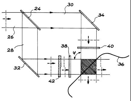
The second setup corresponds to a setup with three
mirrors (see document (1)). In both cases, a
separating splitter 24 (Figure 10) divides a light beam
26 into two identical beams 28 and 30. An
5 interferometric system with two or three mirrors (two
mirrors 32 and 34 in the example in Figure 10)
superposes these two beams 28 and 30 that form a given
angle T, at the fiber 36. The interferences thus
created write the grating in the fiber by cylindrical
10 focusing lenses 38 and 40. The phase splitter 42 needs
to be placed in one of the two interfering beams.
In general, the disadvantage of the amplitude
separation setup is due to the fact that the phase
splitter has to be adjusted each time that the Bragg
15 wavelength is modified since the orientation of the
insolation beam is modified. In order to overcome this
disadvantage, the splitter support device (not shown)
must be controlled along degrees of freedom y and 0
(see above) by a program that takes account of the
setup beam movements necessary for adjustment of the
Bragg wavelength.
We will now consider wave front separation
configurations, and firstly an interferometric setup
with a prism. Note that the method of separating the
wave front has the advantage that the phase splitter
can be placed immediately after the beam expansion
system before the wave front separation. An important
advantage of this configuration is that the phase shift
can be adjusted by rotating the splitter independently
of the Bragg wavelength adjustment that is obtained by
rotating the interferometric system.
B12960.3 PV
CA 02331487 2000-11-09
16
The prism writing method (see document (8)) is
diagrammatically illustrated in Figure 11 in which an
extended beam 44 is "folded on itself" by reflection on
a face of the prism 46. In Figure 11, the reference 48
shows a cylindrical lens. It can be seen that the
determination of the Bragg wavelength fixed by the
inclination of the two interfering beams, can be
adjusted by rotating the prism, against which the fiber
36 is placed. If this rotation is made about an axis
perpendicular to the plane of the Figure and passing
through the phase skip projected in the optical fiber,
then the phase splitter 42 placed on the trajectory of
the beam 44 in front of lens 48, does not need to be
adjusted for the different prism positions.
A wave front separation method that uses a Lloyd
mirror (see document (11)) and that is illustrated in
Figure 12, can also be used. A second return mirror
symmetric to the Lloyd mirror about the center of the
grating, and a CCD camera type position system
sensitive to ultraviolet radiation and particularly to
the writing wavelength (244 nm in our case) is used to
display and adjust the writing beams, in order to
provide more flexibility in adjusting the parameters.
A Bragg grating can be written into an optical
fiber 36 by photosensitivity, advantageously making use
of an frequency doubled argon laser 50 that emits a
beam 52 with a wavelength of 244 nm, but other laser
lines or even other lasers can also be used such as a
KrF excimer laser or a neodymium doped YAG laser
quadrupled in frequency.
B12960.3 PV
CA 02331487 2000-11-09
17
The beam 52 is reflected by a series of mirrors
such as mirror 54 and is then filtered and stretched by
two telescopes, one spherical 56 and the other
cylindrical 58 after passing through a periscope 60.
The beam then passes through the phase splitter 42
placed on a support device 61 with several degrees of
freedom. The beam, in which the wave front has been
modified, is then focused by a cylindrical lens 62 in
the core of the optical fiber 36. This fiber is
located at the edge of the Lloyd mirror 64 that "folds"
the two half-parts of the beam on themselves. Thus,
the beam creates interferences focused in the fiber
core over a length defined by the position of a cover
66. The cylindrical lens 62 and mirror 64 are placed
on two rotation plates 63 and 65 respectively that can
advantageously be motor-driven. Their orientation with
respect to the beam defines the Bragg wavelength of the
written grating. Note that the polarization of the
laser beam is vertical (normal to the work plane).
A second mirror 68, placed symmetrically with
respect to the center of the grating to be written, is
used to display the distribution of intensity writing
the grating. When the beam is focused slightly above
the fiber, the second mirror returns a divergent beam
similar to the beam that is propagated without
reflection. These two parts of the beam are collimated
by a cylindrical lens acting as the inverse of the lens
62 and are finally analyzed by a CCD camera 72 fitted
with an objective 74 with an appropriate magnification.
The distribution of intensity in the plane of the
CCD camera is characteristic of the envelope of the
B12960.3 PV
CA 02331487 2000-11-09
18
intensity distribution of the two half parts of the
beam on the focusing line at the Lloyd mirror.
Provided that the Fresnel diffraction effect between
the grating and the camera can be corrected, this
distribution can be used to determine the envelope of
the beam intensity generating the Bragg grating. This
setup property is used to adjust the position in the
grating of the phase skip(s) (using the y degree of
freedom), with optimum control due to the diffraction
pattern generated by edge effects related to each
thickness change in the phase splitter. When this
adjustment has been made, the laser beam is focused in
the optical fiber and writing the required Bragg
grating can begin.
We will now describe several applications of the
invention for making Bragg grating devices.
A. The invention is applicable to the manufacture
of phase skip Bragg gratings, at high spectral
selectivity.
One of the improvements to the Bragg grating was
to demonstrate a thin secondary transmission band,
called the second transmission peak, in the reflected
wavelength. Thus, the corresponding component, usually
called a "phase skip Bragg grating", transmits a very
specific wavelength from the initial spectrum of the
guided wave in the reflected wavelength band (see
Figure 13, to be compared with Figure 1).
There are many applications of this type of
component in the various fields in which conventional
Bragg gratings are used. It can be used for the
manufacture of matchable lasers and laser diodes. It
B12960.3 PV
CA 02331487 2000-11-09
19
can also be used in wavelength multiplexing and
demultiplexing systems. Furthermore its very good
wavelength selectivity makes it a more efficient
transducer than conventional gratings. Finally, it
forms a new component with its own characteristics that
can easily be applied to solve many guided optics
problems.
Several techniques have been developed to make
this second transmission peak. All use the basic
principle of a phase mismatch between two parts of a
conventional Bragg grating. The guided wave 76 (Figure
14) that passes through a conventional Bragg grating 78
is reflected around the Bragg wavelength a,gragg since the
modulation with period A that forms the grating makes a
distributed reflection of the wave in phase around a
resonance wavelength (in other words a,gragg) given by the
relation kBragg = 2n.A. A constructive interference
phenomenon occurs throughout the length of the grating.
If a phase change is formed at the center of this
type of conventional grating (n = effective mode index)
the two halves of this grating interfere with each
other destructively. The wavelength thus selected can
no longer be reflected and is transmitted in the second
peak. If the transmission is to take place at agraggr
the two parts that interfere must "see" a total phase
shift Ocp equal to 7t (modulo 27t), which is the reason
for the name "7t phase skip Bragg grating".
The desired effect can be obtained if a resonant
cavity 80 with a length such that the total induced
phase shift is equal to 7t, is inserted in the middle of
B12960.3 PV
CA 02331487 2000-11-09
the grating. Thus, we usually consider a phase skip of
n/2, the phase shift due to passing through the cavity.
We can consider a phase shift of X/4, the value of the
optical width of the cavity necessary to produce a
5 forward-return phase shift equal to n.
We can also form a phase change grating. In this
case, the phase mismatch is no longer due to a cavity
but is due to a change in the phase of the periodic
modulation that forms the grating. The result is then
10 identical; a transmission peak appears at the Bragg
wavelength for two modulations with a phase difference
71 with respect to each other. The form of the index
modulation for the case of an amplitude index
modulation Ono with period A along an abscissa z and
15 for a grating of length L, and a phase shift at the
center equal to 0(D, is as follows:
An(z) = Ano.cos(2~z+(D,) for 0 < z < L
A 2
An(z) = Ono.cos(~ z+(D,+0(D) for ~< z < L
We will now study the spectral response of a phase
20 skip Bragg grating. We will consider the case of a
periodic modulation of the propagation index in the
core of an optical fiber. The index modulation is
represented by the following formula:
On ( z ) = Ano . cos (A ?~ z+ cD(z)J
where (D(z) = 0 for 0< z< zt and (D( z) _ A(D for
Zt < Z < Zf.
We will now consider the propagation and counter-
propagation modes A+ and A-. The index modulation will
B12960.3 PV
CA 02331487 2006-12-11
21
act as a disturbance causing coupling between the two
modes. This will be represented by the following coupling
equations:
j ~+ej[2op.Z+~(z)]
dz
dA+ = j f2A-e-j[2op.Z+(D (Z)]
dz
0 is the coupling coefficient at wavelength X in a
fiber with a confinement factor q (proportion of energy
guided in the core and interacting with the grating):
7tAno
~ 71
0(3 represents the phase match between the propagation
wavelength and the resonance wavelength (where n is the
propagation index) : 0(3 = 2~ n- 4~ ~ n.
We will now consider the two conventional Bragg
gratings adjacent to the abscissa z = zt with a phase skip
0(D. The system of equations in the two areas is solved
with the boundary conditions defined in Figure 15:
Ai (0) = 1 AZ (zf) = 0
A+,(zt) = AZ (zt) Ai (zt) = AZ (zt)
The value of IAz(zf)Iz then gives the expression for the
spectral transmission of the grating as a function of the
wavelength, the index modulation Ano, the phase shift A(D
and the lengths of the two areas 1 = zt and 1' = zf - zt
respectively. It is demonstrated that the transmission of
a single phase skip grating can be written:
T(X, Ano, 1, 1') =
Y4
F2 + (C, - r)[C, - I'(1 - 2 cos (0(D) )] + C2 (C2 - 2F sin (A(D) )
CA 02331487 2006-12-11
22
where: 2 = S2Z - 0(3Z L 1+ 1'
S = sinh (y.1) . sinh (y.1' ) C1 = yzcosh (yL)
I' = S22S C2 = 0(3ysinh (yL)
It can easily be checked that the typical
transmission formula for a uniform Bragg grating is
obtained for A(D = 0.
If 0(D =7c and 1 = 1', the formula is simplified to
give:
T = 4
0(32 (0(32 cosh2(yL) + yZ sinh2(yL) - 2522 cosh (yL) ) + SZ4
Note that if the resonant wavelength, A(3 = 0 is
considered, the result is T = 1 regardless of the values
of Ono and L.
If 0(D =7c and 1# 1', the value of the transmission
at the Bragg wavelength is no longer equal to one. The
result is:
T(kBrag9) - cosh2[Q(1 - 1')]
Thus, the transverse displacement of the phase
splitter in the writing beam makes it possible to
precisely define the value of the filter transmission
coefficient at kBragg=
If 0(D # n, the position of the secondary peak in
transmission is no longer matched to the Bragg wavelength.
Different methods are known for manufacturing phase
skip gratings, and particularly the method that
CA 02331487 2000-11-09
23
uses phase change masks. The method used in document
(4) is spatial frequency doubling lithography (SFDL)=
firstly a grating is formed on a mask using the
electron beam emission system (EBES), and the Bragg
grating is then written in the guide by SFDL. Document
(7) describes the phase skip Bragg grating written
using the phase mask method. The mask is composed of a
grating with a phase skip in its modulation period,
which is transmitted by photosensitivity in the fiber
core and the value of the phase skip in the Bragg
grating is fixed by the value of the phase skip in the
mask grating. With this second known method, the
parameters cannot be modified directly and therefore
the cost of a specific and limited implementation is
very high since a mask has to be created for each
spectral position of the grating.
We will now mention the advantages of the
invention for making these phase skip gratings in
optical fibers (but the invention is also applicable to
integrated optical guides):
1. Good manufacturing "flexibility": the
adjustment of the transfer function of the
phase skip grating in transmission, namely the
transmission level and the spectral position of
the peak, is adjusted simply and in a
decorrelated manner. The first adjustment
(transmission) is made by offsetting the
splitter with respect to the insolation wave
half-front (degree of freedom y) and the second
adjustment (spectral position) is made by
rotating the splitter with respect to the beam
B12960.3 PV
CA 02331487 2000-11-09
24
(degree of freedom a or 0). The Bragg
wavelength of the written grating is
independent of the splitter. Therefore, the
splitter can be used to produce the required
spectrum at any position within the normal
wavelength band for this type of application.
This is the main advantage provided by the
process according to the invention compared
with the phase mask method. Furthermore, any
type of grating can be written (for example a
variable modulation pitch grating or an
apodized grating) since the invention only
influences the phase.
2. Control of the result; the different
parameters are adjusted by moving the splitter
(using rotation plates and translation plates,
preferably motor-driven). Since these
movements can be very precisely quantified, the
instrument can give very good control of
grating manufacture.
3. Reproducibility of the manufacturing process is
just as good as for a conventional Bragg
grating written by an interferometric setup
since a phase skip grating is produced in a
single step.
4. Ease of use: it is very easy to use the
instrument, it simply needs to be placed in the
writing beam and the adjustment settings are
made by moving plates. In the same way as for
the phase mask method, the grating is written
B12960.3 PV
CA 02331487 2000-11-09
in a single step, which is also an important
advantage compared with other methods.
5. Production cost: the cost of the apparatus is
not very high since it is not expensive to
5 manufacture a phase splitter by deposition, and
it is relatively easy to install it on a moving
plate. Since the apparatus is also capable of
writing all possible wavelengths, it can also
be considered as being very cost effective. It
10 is also economically attractive since it can be
used to make other components.
Another advantage of this apparatus is related to
its adaptation capabilities. It can thus be used to
write Bragg phase skip gratings in optical fibers or in
15 planar guides or even in semi-conductors. Since the
splitter only influences the phase of the beam,
modifications usually used for writing Bragg gratings
(for example apodization of the spectral response in
order to reduce secondary spectral lobes in the
20 transmission spectrum) can be adapted to the writing
process.
If several phase splitters are placed in the path
of the beam, Bragg gratings with multiple phase skips
can be written, the advantage of which has already been
25 described (see document (13)).
For example, a Bragg phase skip grating has been
written with the following characteristics; grating
length = 10 nm; insolation power = 10 mW; optical
fiber type = hydrogenated SMF28; writing duration = 10
minutes. After writing, the spectrum was analyzed with
a matchable source with a resolution of 1 pm. The
B12960.3 PV
CA 02331487 2000-11-09
26
experimental plot agrees well with the theoretical plot
obtained using the equations described above. The
phase skip is determined by comparing the two plots.
B. The invention is also applicable to the
manufacture of erasable Bragg gratings.
When writing a Bragg grating using an
interferometric method like the methods described
above, it is possible that the Bragg wavelength of the
written grating is different from what is expected.
This is due to the poor reproducibility of these
methods (particularly due to uncertainty about
knowledge of the real writing angle) . It is possible
that the characteristics of the written grating are not
the same as were originally required, due to the lack
of stability of the setup or due to a setting error or
poor knowledge of the effective propagation index of
the guide. In general, the fiber in which this grating
is written must be sacrificed.
One elegant solution for solving this problem is
to be able to erase gratings that do not have the
originally expected characteristics. Thus, test
gratings can be written in a fiber without altering its
spectral properties. In this way, interferometric
methods become more reproducible.
A Bragg grating written in a guide was considered.
It can be represented by the following expression:
2.'K
n (z) = na + Ondver + Ono. cos
n z
Suppose that a grating is then written identical
to the previous grating at the same position, except
B12960.3 PV
CA 02331487 2000-11-09
27
for a phase change equal to n over the grating length.
The result is then:
2.71 2.z:
n ( Z ) =no+Anaver+Ano. cos n Z) +Onaver-On0 = COS ( n z) =no+2 . Onaver
The modulation term has disappeared, and all that
remains is an average increase in the index. If the
transmission spectrum around the Bragg wavelength is
observed, the filtering effect is no longer seen. The
Bragg grating has been erased.
One possible practical solution would be to move
the grating in translation by a half-period in order to
rewrite a grating in phase opposition, but this would
require the use of a translation plate with the
precision of at least 0.1 micrometers (the interference
pitch is usually about 0.5 }zm). Furthermore, the
translation could degrade the focusing setting in the
core.
The invention solves this problem in a very simple
and inexpensive manner. The phase splitter is placed
in the beam using the device with several degrees of
freedom. The position of the phase skip is outside the
grating such that the phase in the grating is constant.
The grating is then written in the same way as if there
had been no splitter. If the decision is made to erase
the grating, then the device is ordered to translate
the splitter to create a phase change of Tt over the
entire grating. For example, for a Lloyd mirror
grating, this is equivalent to placing the phase skip
on the optical axis of the beam, to shift the two
interfering parts out of phase by 7t. This then
prolongs writing until the grating spectrum disappears.
B12960.3 PV
CA 02331487 2000-11-09
28
The final effect is what could be called an opposite
overwriting.
For example, a conventional Bragg grating with a
length of 4 millimeters is written in an hydrogenated
optical fiber (140x105 Pa for three weeks). At a given
writing level, the device is moved in translation in
order to over-write another grating identical to the
first grating, in phase opposition. The reflection
coefficient decreases after translation of the device
to return to its initial value. The grating erase time
is equal to the writing time, and a new grating can be
written continuously once the previous grating has been
completely erased.
We will now describe the advantage of the
invention for making erasable gratings:
1. Good "flexibility": unlike the solution
provided by translation, the setting in this
case is independent of the value of the
modulation pitch and therefore of the grating
wavelength. Since only the phase is changed,
this erasing principle can be applied to all
sorts of gratings (for example chirped
gratings) and phase skip gratings.
2. Control of the result: the phase change
parameter is well-controlled due to the use of
this apparatus. Very high precision is not
necessary for translation of the splitter; 0.1
mm is sufficient. The grating can be erased
with the required precision on the residual
reflection value, provided that the variation
of the spectrum can be monitored in real time.
B12960.3 PV
CA 02331487 2000-11-09
29
3. Reproducibility: reproducibility is not a
problem in this case. Erasing can be done
reproducibly since the phase shift is
controlled.
4. Ease of use: there are no difficulties in
erasing, provided that the change in spectral
characteristics of the grating can be monitored
in real time, since all that is necessary is a
translation control on the splitter support
device and closing of the laser beam at the
right time.
Note that, due to the invention, the writing bench
can be calibrated regularly without modifying the
transmission spectrum of the fiber used to write the
test grating.
Furthermore, erasing the grating is a means of
obtaining a low reflection coefficient at the end of
writing and not at the beginning. Thus, the focusing
adjustment in the core has already been made and does
not disturb growth of the grating.
C. The invention is also applicable to the
production of Fabry-Perot cavity Bragg gratings.
A Fabry-Perot interferometer comprises a cavity
delimited by two mirrors with reflection coefficients
R1 and R2. A matched resonance phenomenon occurs on
the phase shift induced by the cavity when a light wave
with wavelength 4 penetrates into the cavity. When
there are no losses in the two mirrors and R1 = R2 = R,
the intensity at the output from the interferometer is
in the following classical form:
B12960.3 PV
CA 02331487 2000-11-09
I (~) = 1
1 4R 2
+ . .e
sin ?" n cavity
(1-R)2
ncavity is the intra-cavity index assumed to be
equal to one for the case of two mirrors in air and e
is the width of the cavity. The response as a number
5 of waves (6 = 1/k) is a periodic function corresponding
to a comb. The interval between two peaks (or a free
spectral interval denoted ISL) is given by the
relation:
A6
2.n cavity .e
10 The thinness of the lines depends on the value of
the reflection coefficient from the two mirrors and
their height depends on the difference between the two
reflection coefficients.
A Bragg grating may be considered like a mirror
15 about its resonant wave length. It reflects a spectral
band with a given reflection coefficient. If two Bragg
gratings with the same period are put one after the
other, then a Fabry-Perot cavity is created. In the
example of application A, a single secondary peak was
20 added. A series of peaks can be added into the band
reflected by the complete set of the two gratings by
adjusting the distance e between the two gratings.
The fact that a Bragg grating is not a plane
reflector like a mirror, but is rather a reflector
25 distributed over its entire length, implies that the
free spectral interval of a Fabry-Perot cavity grating
is not constant.
B12960.3 PV
CA 02331487 2006-12-11
31
The cavity can be made by opposite overwriting.
Consider a Bragg grating with an index modulation
amplitude Ono/2 with a phase change of 7 at abscissa
z = zl. The total length of the initial grating is denoted
L, the modulation period is denoted A, and the final
average index variation is denoted Anaver. This grating can
be represented by the following index change equation:
On, (z) = A~ eY + A~ . cos( ~ z ) f or 0S z _ zl
An,(z) = An 2ver + A~ . cos( A z) for z15 z_L
Another grating identical to the first grating is
considered but with a phase change at the abscissa zz
(zl <_ z2) . Let An2(z) be the representative function. The
index modulation that will be obtained from the sum of
these two variations is written as follows, with the two
parts of the grating in phase opposition cancelling each
other out:
An(z) = On,(z) + OnZ(z) = Onaver + Ono. cos( A.z)
for 0 5 z S zl
An(z) = On, (z) + An2 (z) = Onaver f or zl < z<_ z2
An(z) = On,(z) + 4n2(z) = Anaõer - Ono. cos( A.z)
for z2 5 z< - L
If z, = L 2 e and z2 = L 2 e, the result will be a
Bragg grating with a Fabry-Perot cavity.
Different methods are known for manufacturing a
Fabry-Perot cavity Bragg grating, particularly as
CA 02331487 2000-11-09
32
described in document (9) in which it is achieved by
writing two successive Bragg gratings at a spacing
equal to the length of the cavity. The match on the
spectral interval and on the position of the peaks is
obtained by uniform insolation of the cavity that
modifies the value of the propagation index in this
area. With this method, the Fabry-Perot cavity grating
has to be written in three steps. In particular, it is
necessary to write two successive gratings, which
increases the manufacturing difficulty.
The invention can be used to make a Fabry-Perot
cavity grating by opposite overwriting. The invention
is a means of positioning a phase skip of 7t in a
grating, an apparatus according to the invention needs
to be placed at a certain abscissa during a time tl and
then at another abscissa during a time t2 in order to
make a Fabry-Perot cavity. An(t) needs to be qualified
during the experimental protocol for making the Fabry-
Perot cavity Bragg grating, in order to determine the
total writing time.
The first step is to determine the experimental
conditions for the Fabry-Perot cavity grating to be
written; the lengths 11 and 12 of the two Bragg
gratings and their reflection coefficients R1 and R2,
the length of cavity e, the fiber type and the
insolation power. All these parameters are used to
plot the spectrum using a matrix method (see document
(12)) and thus to predict the shape of the spectral
response of the Fabry-Perot cavity grating. The length
of the cavity and the value of the average index change
B12960.3 PV
CA 02331487 2000-11-09
33
need to be known to determine the free spectral
interval. The following procedure can be used:
Ono is deduced using the following relation:
~n0 = k Bragg arg talh( R. ) where i = 1, 2
7Z.Y1.1 i
where rl is the confinement factor for the wave guided
in the core. The total length L of the grating is
given by L 11 + e + 12. There is a reflection
coefficient R corresponding to this length L and this
index modulation, given by:
~.On
R = tanh .~.L
a' Bragg
Therefore, a grating with length L is written to
obtain a reflection coefficient R. Let the measured
insolation time be ttotal. During this writing, the
Bragg wavelength was offset by OXBragg corresponding to
the increase in the value of the average index Anaver:
~ Bragg
Onaver =
2.A
The free spectral interval can thus be determined:
06 = l
2.(110 +Ariaver).e
There are two possibilities if the value of the
ISL is not suitable; either e can be changed and
writing can be repeated to determine the new value of
ttotal, or the process can be continued and writing can
be finished by a uniform insolation of the cavity which
will have the effect of increasing the average index.
The insolation times for the two gratings with
opposite phases are equal: tl = t2 = t' 'a]
2
B12960.3 PV
CA 02331487 2000-11-09
34
The first two test gratings can be erased using
the method described above. We can now write the
Fabry-Perot cavity grating. The phase skip is placed
at a distance 11 from the edge of the grating using an
apparatus conform with the invention, a grating is
written for a time tl, and the splitter is then moved
by translation using its support device over a distance
e, and writing is prolonged by a time t2. The Fabry-
Perot cavity Bragg grating is written.
We will describe the advantages of the invention
for making this type of Bragg grating.
1. Manufacturing "flexibility": any Bragg
wavelength can be written, in the same way as
for the phase skip grating. The cavity length
and the length of the two gratings is limited
by the maximum size of a Bragg grating that can
be written by the interferometric setup used.
It is not limited by the apparatus, which
includes a means of adjusting the length of the
cavity with the precision possible by the
adjustment in y. The reflection coefficients
of these two gratings can be chosen by varying
the total writing duration and the relative
length of the two gratings. Therefore, it can
be seen that most of the parameters are
accessible with good "flexibility".
2. Reproducibility: there is no reproducibility
problem related to the value of the wavelength
of the two Bragg gratings since they have the
same period. This is an advantage compared
with known methods.
B12960.3 PV
CA 02331487 2000-11-09
D. The invention is also applicable to the
manufacture of a Bragg grating with a particular index
modulation envelope.
The equation for a non-uniform Bragg grating can
5 be written in the following form:
2.71
On ( Z ) =0naver ( Z ) + Anmod ( Z ) . COS -.Z
Onavery(Z) is the average index distribution (as a
function of the abscissa z), Anmod(z) is the index
modulation envelope of the Bragg grating, and A is the
10 modulation period;
More sophisticated components can be obtained by
making non-uniform gratings. For example, it is often
desirable to apodize the gratings. The transmission
spectrum of an apodized grating includes very small
15 bounce on each side of the central peak, making it a
particularly attractive component for all types of
applications.
We will now consider the principle of dynamic
phase shifted overwriting; we will use the basic
20 principle presented in application examples B and C
(successive writing of two gratings with parts in phase
opposition), except for the difference that overwriting
is done for variable times and for variable phase skip
positions and values. Analytically, this is equivalent
25 to considering a grating growth defined by the
following relation:
An (z, T) = la (z,t)+b (z,t) . co42~n. z+0(Z,t)), dt
0
where a(z,t) = a0r~ver (z,t) and
B12960.3 PV
CA 02331487 2000-11-09
36
b(z,t) = aAn am d (z,t)
a(z,t) characterizes the growth kinetics of the
average index change in the grating,
depending on a large number of parameters
(for example the insolation power and fiber
type) and can be determined by studying the
variation of the Bragg wavelength while
writing a test grating.
b(z,t) characterizes the growth kinetics of the
index modulation envelope in the grating,
and depends on many parameters and can be
determined by studying the variation of the
maximum reflection coefficient while
writing a test grating.
(D (z,t) is the function defined by the position and
inclination of the splitter(s). This is a
step function.
The variation of the average index cannot be
modified using the invention. Therefore, we will only
use the value of the index modulation:
Onper. (z, T) = T b(z,t).cos ~.z+~(z,t) .dt
0
We can write:
Onpe r.( z, T) = f[b(z, t).cos((D(z, t)ldt .cosC 2=" z
A
J
0
T
- {[b(z, t).sin(~(z, t)]~dt .sin( n.z
o
It can be seen that the modulation term is the sum
of two amplitude modulations determined by the function
B12960.3 PV
CA 02331487 2000-11-09
37
(D (z,t). A special application case is given when the
value of a) is 0 or 7c. Firstly, we will consider a
dynamic opposite overwriting with a single skip. We
can define:
(D(z,t) _n if 0<_ z 5 zn(t)
(D(z,t) = 0 if zn (t) S z< L (L = length of the
Bragg grating).
The zn(t) function defines the phase skip
movement. The grating growth at abscissa z is a
function of the phase shifted modulation time (t,t(z))
or the unshifted modulation time (to(z)) applied to the
elementary part of the grating. The total writing time
is denoted T. The final index modulation amplitude of
the grating at abscissa z is denoted OnTmod(Z) . We can
write:
to(z) T
OnTmod ( z)= J b(z, t).dt - Jb(z, t- t o(z)).dt
0 to(z)
The standard modulation envelope A(z), is defined
as Onmod(z)=OnoxA(z) . In general, the minimum value of
this function is denoted Ao. A(z) is the function to
be obtained in the grating. This cannot be done unless
the growth dynamics of the index modulation are known.
It will be assumed that this growth function is known
and is independent of the abscissa in the grating. We
will set:
to
An mod (t 0)= J b(t) . dt
0
hence:
B12960.3 PV
CA 02331487 2000-11-09
38
A (z) = On mod (T - t 0(Z)) Anmod lt o(Z)~
Ano Ano
Thus, there are two possible cases that correspond
to two choices of the phase skip movement (move then
rest or rest then move). These two movements give
exactly the same result.
We will now consider the case:
A(Z) = An mod (T - t 0(Z)) On mod \t 0 (Z))
Ono Ono
This choice defines the time interval of the phase
skip movement:
A ( z ) ?Ao implies Onmod (to ( z ) ) < Anmod ( T-to ( z ) ) - OnoxAo
which implies to (z) <_ tsõp
A(z)-1 implies Onmod(to(z) )? Onmod(T-to(z) ) - Ono which
implies to ( z ) < tinf
We can deduce:
z,,(t) = A-1 (1) for 0<-t<-tinf
zn (t) = A-1 rAnmod(T-1)Anmod(t) for
Ono Anp
tinf<t<tsup
zn (t) = A-1 (Ao) for tsup<_t<-T.
Therefore, we can see that making an index
modulation according to function A(z) in the case of a
method with dynamic opposite overwriting with a single
skip is only possible if A(z) is a reversible function.
If A(z) is not defined over a bijection interval,
another method has to be applied. This interval has to
be broken down into bijection parts. The number of
phase skips to be placed in the beam is then equal to
the number of the bijection intervals.
B12960.3 PV
CA 02331487 2000-11-09
39
Let N be the number of bijections, and let i be
the number of bijection interval of A(z) [zi-1; zi].
We can define dno: dno = max(Ono.A(z)) in [zi-l;zi]
and Ai (z) as an application of [0; zi-zi-1] in [0; 1]
which associates dn dn. A( zi-1 + Z) with Z.
o
This problem is solved in the same way as in the
case of a single skip. This is done by determining the
movement of N phase skips by applying the formulas to
series of functions Z' T (t) defined with respect to each
origin zi_1. Therefore, regardless of the shape of
A(z), the dynamic opposite overwriting method with
multiple skips can be used to produce the corresponding
grating.
We will now consider the production of a
particular index modulation envelope according to the
invention. The y translation of the splitter support
device can be used to position the phase skip at any
place in the grating. Therefore, a software controlled
motor can control the movement zn(t) and thus induce a
modification to the grating index modulation envelope.
If the function A(z) is not defined over a
bijection interval, it is possible to place a series of
devices provided with splitters in sequence to make the
modification using the multiple skips method. In the
same way as for a single support device, the various
motors can be controlled to make the component. This
production requires precise knowledge of the grating
growth function, Onmod(t). This knowledge can be
obtained by studying a test grating for which the
B12960.3 PV
CA 02331487 2000-11-09
variation of the reflection factor is measured with
respect to time. This measurement must be made at the
same power as the power that will be used later to make
a grating in the form A(z). The required function is
5 deduced using the following relation:
Anmod (t)=~ Bragg arg t111h( R't))
7r. 1. L
(see above for writing a Fabry-Perot cavity Bragg
grating).
More simply, the function A(z) may be approximated
10 by assuming the growth of the modulation index to be
linear with respect to time. In this case, the
formulation of the equations is very much facilitated.
We will now describe the advantage of the
invention for making a Bragg grating with a particular
15 index modulation envelope.
1. Manufacturing "flexibility": a Bragg grating
with a constant or chirped spatial period can
be written at any Bragg wavelength and any
shape of index modulation or average index
20 envelope, provided that an appropriate number
of support devices equipped with phase
splitters are placed.
2. Ease of use: it is easy to produce the
grating. All that is necessary is to measure
25 the growth function of a grating at a given
power, and then to invert the function A(z) to
be produced. Each splitter support device,
with its control software installed on it, then
manages displacement of the corresponding
30 splitter.
B12960.3 PV
CA 02331487 2000-11-09
41
Note that the growth function of the modulation
index with respect to time may be determined
experimentally.
We will now give a few example applications.
The case of a linear approximation is considered,
to describe them easily Onmod(t) = a.t.
a) We can attempt to write a grating with a linear
modulation envelope of the type shown in Figure 16.
The phase skip movement for a linear approximation is
defined as follows:
Z7c(t)- T.t for 05 tT and
z,~(t) = L for ~_< tT.
b) An attempt can be made to apodize a Bragg
grating. A gaussian envelope is chosen:
A(z) = exp[-(z-L/2)2/(L/N)2]
The shape of the grating when N = 4 is as shown in
Figure 17. This shape is used to apodize the grating,
or more precisely its spectral response. The secondary
lobes in the reflection spectrum for this grating are
smaller than with a conventional grating.
In the example considered, A(z) is not defined
over a bijection interval. Therefore, two functions
are defined:
Interval 1: [0; L/2] :
A1 (z) = exp[- (z-L/2) 2/ (L/N) 2] for z within [0; L/2]
Aa=0
An'o = Onmod (T)
Interval 2: [L/2;L]
B12960.3 PV
CA 02331487 2006-12-11
42
Al(z) = exp[- (zz / L/ NZ] for z within [0; L/2]
Aa = 0
An0 = Anmod (T)
We can deduce the movement of the two phase skips:
Interval 1:
z'n(t) = L. 1-?. ln T for 0t< T
2 N 2.t) 2
z,'n(t)=0 for ~ St - T
Interval 2:
z~(t) = L . 1 + 2 , ln( T I for 0 t< T
2 N T-2.t1 2
zn(t) = L for ~<_ t< T
The following documents are referenced in this
description:
(1) C.G. Askins, T.E. Tsai, G.M. Williams, M.A.
Putnam, M. Bashkansky and E.J. Friebele, "Fiber Bragg
reflectors prepared by a single excimer pulse", Optics
Letters, 17, 11, (1992), pp. 833-835.
(2) F. Bilodeau, K.O. Hill, B. Malo, D.C. Johnson and
J. Albert, "High-return-loss narrowband all-fiber bandpass
Bragg transmission filter", IEEE Phot. Tech. Lett, 6, 1,
(1994), pp. 80-82.
(3) I. Baumann, J. Seifert, W. Nowak and M. Sauer,
"Compact all-fiber Add-Drop-Multiplexer using Fiber
CA 02331487 2000-11-09
43
Bragg Gratings", IEEE Phot. Tech. Lett., 8, 10, (1996),
pp. 1331-1333.
(4) C.H. Henry, Y. Shani, R.C. Kistler, T.E.
Jewell, V. Pol, N.A. Olsson, R.F. Kazarinov, K.J.
Orlowsky, "Compound Bragg reflection filters made by
spatial frequency doubling lithography", J. Lightwave
Technol., 7, 9, (1989), pp. 1379-1385.
(5) K.O. Hill, D.C. Johnson, F. Bilodeau and S.
Faucher, "Narrow-bandwidth optical waveguide
transmission filters", Electron. Lett., 23, 9, (1987),
pp. 465-466.
(6) R. Kashyap, G.D. Maxwell et B.J. Ainslie,
"Laser-trimmed four-port bandpass filter fabricated in
single-mode photosensible Ge-doped planar waveguide",
IEEE Phot. Tech. Lett., 5, 2, (1993), pp. 191-194.
(7) R. Kashyap, P.F. McKee and D. Armes, "UV
written reflection grating structures in photosensitive
optical fibres using phase-shifted phase masks",
Electron. Lett., 30, 23, (1994), pp. 1977-1978.
(8) S. Legoubin, M. Douay, P. Bernage, P. Niay,
J.F. Bayon and T. Georges, "Photoinscription de filtres
de Bragg dans des fibres dopees a l'oxyde de germanium"
(Photo-writing Bragg filters in fibers doped with
germanium oxide), J. Optics, 23, 4, (1992), pp. 143-
156.
B12960.3 PV
CA 02331487 2000-11-09
44
(9) S. Legoubin, M. Douay, P. Bernage, P. Niay,
J.F. Bayon, T. Georges, J. Opt. Soc. Am., A12, (1995),
P.1687.
(10) G. Meltz; W.W. Morey and W.H. Glenn,
"Formation of Bragg gratings in optical fibers by a
transverse holographic method", Optics Letters, 14,
(1989), pp. 823-825.
(11) I. Riant, P. Sansonetti, H. Fevrier, A.
Artigaud, "Realisation d'un filtre de Bragg photo-
inscrit dans une fibre optique a l'aide d'un montage
interferometrique constitue d'un miroir unique"
(Production of a photo-written Bragg filter in an
optical filter using an interferometric setup composed
of a single mirror), Paper presented at the JNOG,
(1993), Marseilles, Session 2.
(12) M. Yamada and K. Sakuda, "Analysis of almost-
periodic distributed feedback slab waveguides via a
fundamental matrix approach", Applied Optics, 26, 16,
(1987), pp.3474-3478.
(13) R. Zengerle and 0. Leminger, "Phase-shifted
Bragg-Grating Filters with Improved Transmission
Characteristics", J. Lightwave Technol., 13, 12,
(1995), pp.2354-2358.
B12960.3 PV