Note: Descriptions are shown in the official language in which they were submitted.
CA 02331610 2000-11-08
WO 9915901 I PCT/US99/10564
MICRO-LASING BEADS AND STRUCTURES, AND ASSOCIATED METHODS
CLAIM OF PRIORITY FROM COPENDING PROVISIONAL PATENT
APPLICATIONS:
Priority is herewith claimed under 35 U.S.C. ~119(e) from
copending Provisional Patent Application 60/085,286, filed
5/13/98, entitled "Cylindrical Micro-Lasing Beads for
Combinatorial Chemistry and Other Applications", by Nabil
M. Lawandy; Provisional Patent Application 60/086,126,
filed 5/20/98, entitled "Cylindrical Micro-Lasing Beads for
Combinatorial Chemistry and Other Applications", by Nabil
M. Lawandy; Provisional Patent Application 60/127,170,
filed 3/30/99, entitled "Micro-Lasing Beads and Structures
for Combinatorial Chemistry and Other Applications,
Including Techniques for Fabricating Same", by Nabil M.
Lawandy; and from Provisional Patent Application
60/128,118, filed 4/7/99, entitled "Search, Point and Shoot
Technology for Readout of Assays", by Nabil M. Lawandy. The
disclosure of each of. these four Provisional Patent
Applications is incorporated by reference herein in its
entirety.
FIELD OF THE INVENTION:
This invention relates generally to beads and other
structures typically used in combinatorial chemistry
applications, as well as to structures capable of emitting
electromagnetic radiation, and to optical encoding
techniques and to techniques for reading out and detecting
encoded information.
CA 02331610 2000-11-08
WO 99/59011 PCT/US99/10564
2
BACKGROUND OF THE INVENTION:
In an article entitled "Plastic microring lasers on fibers
and wires", Applied Physics Letters, Vol. 72, No. 15, pp.
1802-1804, 13 April 1998, S.V. Frolov, Z.V. Vardeny, and K.
Yoshino demonstrate that photopumped, pulsed, narrow laser
emission lines with very low threshold excitation
intensities can be obtained using luminescent conducting
polymer (LCP) films deposited around thin optical fibers
and metal wires. For the laser active material the authors
l0 chose a derivative of polyp-phenylene-vineylene) (PPV),
namely, 2,5-dicetyloxy PPV (DOO-PPV), which has been shown
to be an excellent laser-active medium in the red/yellow
spectral range. The lowest excited states in DOO-PPV are
excitons with energy levels similar to those of organic
laser dyes, which under optical excitation form a four-
level laser system. The polymer laser transition then
occurs at longer wavelengths compared to the pump
wavelength, and thus, population inversion can be achieved
at relatively low excitation densities.
In a combinatorial chemistry application a large number of
so-called solid supports or beads are provided so as to
have a matrix or growth matrix phase (also referred to as
a functionalized support) to which various compounds can
adhere during the synthesis of diverse new compounds, some
of which have, ideally, useful physiological or other
properties. A problem in the use of such beads is in
providing an identification for the beads that facilitates
the subsequent screening and identification of, for
example, an oligomer sequence that is synthesized.
OBJECTS OF THE INVENTION:
It is an object of this invention to provide an improved
structure useful in combinatorial chemistry and other
applications, the structure employing one or more optical
gain medium layers or films deposited around or over a
CA 02331610 2000-11-08
WO 99/59011 PCT/US99/10564
3
core.
It is a further object of this invention to provide a
technique for fabricating structures suitable for use in
combinatorial chemistry and other applications, wherein the
5 structures comprise regions of optical gain medium capable
of providing each structure with a characteristic optical
emission signature.
It is another object of this invention to provide an
optically-based technique to excite optical gain mediums
10 disposed on the structures, and to detect the
characteristic optical emission signature from different
ones of the structures.
SUMMARY OF THE INVENTION
15 A structure in accordance with an aspect of this invention
can include a core or other substrate, at least one and
preferably a plurality of optical gain medium films
disposed about said core for providing a plurality of
characteristic emission wavelengths. The structure may
20 further include a functionalized support suitable for the
synthesis therein or thereon of a chemical compound.
Various structure geometries are disclosed, such as disks
and spheres, as well as several suitable pump sources and
detectors. A technique for fabricating planar-type
25 structures is also disclosed, wherein a micro-laser bead
structure contains a plurality of areas or dots of optical
gain material and is contained between protective
substrates using, for example, a solvent resistant cross-
linked polymer adhesive. At least one of the protective
30 substrates is substantially transparent (at the excitation
and emission wavelengths of interest) and is disposed
between a substrate surface that bears the micro-laser dots
and the environment.
CA 02331610 2000-11-08
WO 99/59011 PCT/US99/10564
4
In one embodiment a method employs a head with one or more
orifices for selectively printing optical gain material
into the areas, and a mechanism for causing relative motion
between the head and the substrate. The step of depositing
5 may deposit a full complement of optical gain material into
each of the plurality of areas. In this case the method
includes a step of selectively removing (e. g., mechanically
removing or laser or photo-ablating) or deactivating (e. g.
optically photo-bleaching) the optical gain material within
10 selected ones of the areas.
The substrate may have a large size for fabricating many
micro-laser bead structures, which are then physically
separated by sawing or dicing, in a manner similar to that
used in integrated circuit fabrication.
15 Also disclosed is a bead of a type that includes a
functionalized support (a growth matrix suitable for use in
at least a combinatorial chemistry application), and that
further includes a gain medium coupled to a structure that
supports the creation of at least one mode for
20 electromagnetic radiation, and/or which has a dimension or
length in one or more directions for producing and
supporting amplified spontaneous emission (ASE). The
structure can have boundaries that impart an overall
geometry to the structure that, in combination with at
25 least one material property of the structure, supports an
enhancement of electromagnetic radiation emitted from the
gain medium by favoring the creation of at least one mode
that enhances an emission of electromagnetic radiation
within a narrow band of wavelengths. Information is encoded
30 into the bead using only wavelength encoding, or by using
both wavelength encoding and signal level encoding. The
information may be encoded using one of a single level
encoding or multi-level encoding.
CA 02331610 2000-11-08
WO 99/59011 PCT/US99/10564
BRIEF DESCRIPTION OF THE DRAWINGS
The above set forth and other features of the invention are
made more apparent in the ensuing Detailed Description of
the Invention when read in conjunction with the attached
5 Drawings, wherein:
Fig. lA is an enlarged elevational view of a micro-lasing
cylindrical bead structure;
Fig. 1B is an enlarged cross-sectional view of the micro-
lasing cylindrical bead structure;
l0 Fig. 2 is a graph that depicts an exemplary lasing emission
from the micro-lasing cylindrical bead structure;
Fig. 3 is an enlarged cross-sectional view of a micro
lasing cylindrical bead structure capable of emitting three
distinct wavelengths and including a functionalized
15 support.
Fig. 4 is an enlarged cross-sectional view of a spherical
geometry micro-lasing structure, in accordance with one
embodiment, or a top view of a disk-shaped micro-lasing
structure in accordance with another embodiment;
20 Figs. 5-9 each depict an embodiment of a laser-based
optical system that employs Raman Scattering for generating
all or some of multiple pump wavelengths;
Fig. 10 is a schematic diagram of a Raman laser module
using a Nd:YLF pump laser;
25 Fig. 11 is a graph that illustrates a typical output
spectrum of the Raman laser module of Fig. 10;
Fig. 12 is a graph that plots power out versus power in,
CA 02331610 2000-11-08
WO 99/59011 PCT/US99/10564
6
and thus illustrates a slope efficiency curve for the Raman
laser module of Fig. 10;
Fig. 13 is a block diagram of an embodiment of a pump
source/reader system;
Fig. 14 is a block diagram of a lasing bead structure
fabrication print step;
Fig. 15 is an enlarged cross-sectional view of a lasing
bead structure laminate with a solvent resistant cross-
linked polymer;
l0 Fig. 16 shows further lasing bead structure fabrication
steps, wherein Fig. 16A shows an integrated solid support,
Fig. 16B shows attachment of resins, such as commercially
available LLC Dynospheres, by flexographic, intaglio, or a
reverse analox roll process, and Fig. 16C shows direct
grafting of the functionalized support;
Fig. 16D depicts a further embodiment wherein resin beads
are placed into wells and fixed in place with a mesh
structure, while Fig. 16D shows a multi-chip composite
structure;
Fig. 17 is a top view of wafer containing a plurality of
lasing bead structures, and a wavelength calibration and
slicing of the wafer into individual lasing bead
structures;
Fig. 18 depicts an exemplary Lawn Assay readout technique
in accordance with an aspect of this invention;
Fig. 19 illustrates a substrate having embedded fibers or
threads that emit narrow-band light, when exited by an
optical source such as a laser, containing one or more
CA 02331610 2000-11-08
WO 99/59011 PCT/EJS99/10564
7
characteristic wavelengths;
Fig. 20A illustrates a planchette embodiment of a bead
suitable for use in a combinatorial chemistry, or other
application, in accordance with the teachings of this
invention;
Fig. 20B illustrates a filament or fiber embodiment of a
bead in accordance with the teachings of this invention,
and which is suitable for embodying the threads shown in
Fig. 19;
Fig. 20C illustrates a distributed feedback (DFB)
embodiment of a bead in accordance with the teachings of
this invention;
Fig. 20D illustrates a top view of a planchette, as in Fig.
20A, or an end view of fiber, wherein the planchette or
fiber is sectored and capable of outputting multiple
wavelengths;
Fig. 20E illustrates a top view of a planchette, as in Fig.
20A, or an end view of fiber, wherein the planchette or
fiber is radially structured so as to be capable of
outputting multiple wavelengths:
Fig. 21 is an enlarged, cross-sectional view of an
embodiment of a bead that is also suitable for embodying
the threads shown in Fig. 19;
Fig. 22 is an enlarged, cross-sectional view of an other
embodiment of the bead of Fig. 21;
Fig. 23 depicts the emission peak of a selected dye in any
of the embodiments of Figs. 20A-20E, before (B) and after
(A) a spectral collapse;
CA 02331610 2000-11-08
WO 99/59011 PCT/US99/10564
8
Fig. 24 shows characteristic emission peaks for a thread
comprised of a plurality of constituent polymeric fibers,
each of which emits at a characteristic wavelength;
Fig. 25 is a graph that illustrates a number of suitable
5 dyes that can be used to form the gain medium in accordance
with this invention;
Fig. 26 is a simplified block diagram of one embodiment of
a bead identification system that is an aspect of this
invention;
i0 Fig. 27 is a simplified block diagram of a further
embodiment of a bead identification system that is an
aspect of this invention; and
Fig. 28 depicts emission wavelength signal amplitude and is
useful in explaining an embodiment of this invention
15 wherein both wavelength and signal level amplitude coding
are employed.
DETAILED DEBCRIPTION OF THE INVENTION
Referring to Figs. lA and 1B, cylindrical dielectric sheet
structures are equivalent to a closed two dimensional slab
20 waveguide and support a resonant mode. Modes with Q values
exceeding 106 are possible with active layer thicknesses of
1-2~,m and D-Sum-50~Cm. The structure may be constructed in
a similar manner to that described by Frolov et al. so as
to include a LCP layer or film.
25 Referring to Fig. 2, the presence of amplifying media in
the guiding region results in laser oscillation with
emission spectra narrower than about 1 Angstrom. Unlike
fluorescence, the lasing emission signature of the micro-
lasing bead is non-saturable and leads to detection with
30 high signal to noise ratios.
:,
CA 02331610 2000-11-08
WO 99!59011 PCT/US99/10564
9
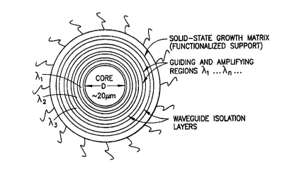
Referring to Fig. 3, the cylindrical geometry is ideal for
producing multi-wavelength (e.g. , .li, ~lZ, ~1~) laser emission
from micro-lasing beads. The core region can be metallic,
polymeric or scattering. The cylindrical geometry allows
5 for the use of economic extrusion and coating techniques in
the manufacturing of each micro-lasing bead code. Note that
the bead includes a solid-state functionalized support
layer or region, making it suitable for use in
combinatorial chemistry applications such as the one
l0 described above.
The typical amplification coefficients required are in the
100cm'~ range resulting in optical pump absorption depths
of 50~m-100~m. This allows for as many as N=30 different
lasing layers in a single micro-lasing bead. A possible
15 constraint of a 50um transverse dimension, along with a
waveguide isolation region (~l~cm) , leads to N-6 possible
wavelengths from a single bead.
The lasing optical bit number (M) for micro-lasing beads is
set by the excitation sources, detection range, and the
20 required wavelength spacing (<lnm) . By example, for a 532nm
excitation at the short wavelength side and silicon
detector response at the long wavelength side (900nm), one
has M-350. A binary coding scheme with up to N bits out of
a total of M possibilities leads to a coding capacity t.
25 Reader systems which have direct applicability in
combinatorial chemistry and HTS applications enable the
reading of the wavelength signatures of the beads. The
wavelength range and code capacity of the cylindrical
micro-lasing beads can be extended using compact and
30 intense nanosecond sources extending throughout the silicon
detector range. The excitation source can preferably
spatially locate and laser excite individual micro-lasing
in a wide field of view.
CA 02331610 2000-11-08
WO 99/59011 PCT/US99/10564
While described thus far in the context of LCP material as
a gain material, other gain materials may be used as well.
Other suitable gain medium materials include, but are not
limited to, semiconducting polymers, PPV, methyl-PPV, etc.;
5 dye-doped polymers, sol-gel glasses, and many other
glasses, such as semiconductor-doped glasses; and
stimulated Raman media. In general, any gain medium can be
used that has a higher index of refraction than the core
and the surrounding isolation layer(s).
10 The teachings of this invention are not limited to only
elongated, cylindrical structures. For example, and
referring to Fig. 4, a generally spherical geometry can be
provided, in an "onion-skin" embodiment, with one or more
gain material layers and isolation layers. Each generally
spherical micro-lasing bead can be used in a combinatorial
chemistry or some other application.
Furthermore, the structure could be manufactured in an
elongated fiber form and then cut into disk-shaped
structures. In this case a minimum disk thickness would be
on the order of one half wavelength.
Any suitable pump source can be employed. For a multi-
wavelength emission case one or more pump sources may be
required, or a single pump source that is capable of
emitting a plurality of wavelengths. A dye laser is one
such example.
Further in accordance with this invention another suitable
multi-wavelength pump source employs efficient stimulated
Raman Scattering in narrow linewidth, high Raman cross-
section salts such as Ba (NO3) z, Ca (C03) and NaN03 ( in
general: RX(M03)y). Such a source can be used to create an
all solid state, compact, low cost and low maintenance pump
source for exciting the bead structures. The preferred
r
CA 02331610 2000-11-08
WO 99/59011 PCT/US99/10564
11
crystals have Raman gains of the order of 10-50 cm/GWatt '
and exhibit excellent transparencies with typical shifts in
the 1000-1100 cm-~ range (e.g. , Ba (N03) z gives 1047cm-~) . In
addition, the Raman process is not phase matched so that
5 the source is extremely insensitive to crystal vibrations,
translations and rotations. Typical costs for such crystals
can be as $1000 or less, and simple single pass gain or
resonant cavity designs are adequate for most if not all
applications. Furthermore the use in some embodiments of a
10 robust Nd:YAG laser to drive all of the required
wavelengths results in greatly improved life and service
requirements.
Fig. 5 shows a first embodiment of an all solid state
optical source to for that is capable of providing red-
15 green-blue (RGB) pump wavelengths. The source 10 uses a
single Q-switches Nd:YAG laser that outputs 1.06 micrometer
light, an external frequency doubler, such as a KTP crystal
to produce 532 nm light, a further non-linear crystal to
generate 355 nm light, and two resonant cavity Raman
20 Scattering structures each using a selected one of a
Rx (MO3) Y crystal to generate the red and the blue light. The
green light is generated directly from the 532 nm frequency
doubled Nd:YAG output.
Fig. 6 shows a second embodiment of an all solid state
25 optical source 20 that uses an intra-cavity doubled Q-
switched Nd:YAG laser and a separate Q-switched Nd:YAG
laser. The two lasers are electrically and delay
synchronized such that combined pulses are applied to a
non-linear crystal in the blue light Raman channel. The red
30 light is generated by a second Raman scattering resonant
cavity structure from the 532 nm light, while the green
light is obtained directly from the 532 nm light. This
approach is capable of providing higher powers than the
embodiment of Fig. 5.
CA 02331610 2000-11-08
WO 99/59011 PCT/US99/10564
12
The embodiment 30 of Fig. 7 uses only 532 nm light and
Coherent Anti-Stokes Raman Scattering (CARS) to produce the
blue emission. The red and the green emissions are
generated in the manner shown in Fig. 6.
The embodiment 40 of Fig. 8 uses Raman shifting for both
the blue and red emissions.
The embodiment 50 of Fig. 9 uses the Anti-Stokes which is
emitted as a ring or "donut" mode from the resonator. This
ring is then converted by a diffractive optical element
into a solid spot, thus providing the solid state RGB
source with a single laser source. It should be noted that
the inventor observed up to the fourth Stokes (Z~o - 4T~R) and
the third Anti-Stokes, without using the resonator.
Fig. 10 illustrates a Raman Laser Module 60 that employs a
Nd:YLF pump laser. The mirrors in the Raman cavity are as
follows. The output coupler is highly reflecting from 527-
590 nm, and has R=70% at 630nm. The input coupler is
highly transmissive at 527 nm and highly reflective from
557-630 nm. The input coupler has a concave radius of
curvature of 10 cm, and the output coupler is flat. This
configuration is, of course, only an example for the 5 cm
barium nitrate crystal that was used in the cavity.
As but one example, a Photonics Industry Nd:YLF laser is
operated at a PRR of 300 Hz and a PW of 200 nsec. The
630/527 nm slope efficiency is about 17.5% with the maximum
630 nm power = 330 mW at 2.4 W green input.
Fig. 11 is a graph that illustrates a typical output
spectrum of the Raman laser module of Fig. 10: and Fig. 12
is a graph that plots power out versus power in, and thus
illustrates a slope efficiency curve for the Raman laser
module of Fig. 10.
CA 02331610 2000-11-08
WO 99/59011 PCT/US99/10564
13
Referring to Fig. 13, a device 70 for reading the emission
wavelengths can be comprised of a spectrometer, preferably
a monolithic spectrometer 72. Such a device may comprise an
optical fiber 74 and a prism or grating 76 for enabling
5 individual wavelengths emitted by a single lasing structure
or bead to be resolved and identified through the use of a
multi-pixel detector 78, such as a CCD array. A look-up
table (LUT) 80 can be used to output a code or bead
identification (bead ID) corresponding to the detected
10 wavelength(s). The laser source 82 for the reader device
could be any one of the various sources referred to above.
One suitable spectrometer is one referred to as a S2000
Miniature Fiber Optic Spectrometer that is available from
Ocean Optics, Inc.
15 The teachings of this invention also encompass the use of
a reader with a search phase, a targeting, or pointing
phase, and a laser excitation phase (i.e., Search, Point
and Shoot (or SPS), such as one based on or similar to the
ones described in commonly assigned U.S. Patent Application
20 Serial Number 09/197,650, filed 11/23/98, entitled "Self-
Targeting Reader System for Remote Identification" by
William Goltsos, the disclosure of which is incorporated by
reference herein in its entirety. This type of reader
system may be used to quickly read out the results of any
25 "reporter" assay in a one, two, or three dimensional field.
In one example, a Lawn Assay using E-coli (or other
bacteria) and a reporter gene (e. g., a green fluorescent
protein or a chemiluminescent assay) can be used to provide
an optical signature correlated to a specific target, when
30 a compound-containing solid support is placed on it.
Optically coded beads with synthesized material are
deposited at random on the medium (e. g., agar), resulting
in about a 6mm to emm zone of activity that arises from a
successful assay. This activity further results in
s,
CA 02331610 2000-11-08
WO 99/59011 PC'T/US99/10564
14
fluorescence which is detected by the search phase (e. g.,
a camera digitization of intensities with a defined range '
and/or affected zone parameters (e.g., radius, etc.)) The
SPS then points to or targets the bead and then illuminates
(shoots) it with a laser pulse sufficient to read its
optical code. The optical code could arise from a lasing
material or fluorescing material on the bead, such as those
described above and/or described below in the planar
embodiment.
l0 The SPS system can then read the Lawn Assay at a rate of
about 2o msec/bead, a time which is several orders of
magnitude faster than is possible with currently available
millimeter or submillimeter scale element or solid support
bead. In addition, no handling is required to read the
code, such as manipulation for chemical or mass
spectroscopy deconvolution.
The method can use thresholding to set the level of assay
activity, allowing for the screening of different levels of
activity. This allows users to refine their understanding
of which molecular parameters (e. g., ring position) create
activity for a specific (drug) target.
For other assays, such as direct binding or fluid based
assays, the search phase can be replaced by any source of
coordinates. For liquid systems in assays, beads located
in sample plate and other types of wells can be read out by
coordinates which are supplied to the point and shoot
stages. For x-ray and Y-ray radioactive assays,
coordinates can be obtained from CCD arrays (e. g., those
comprised of amorphous silicon) or from scintillation
plates to create a signal for the optical point phase.
Other assays which create temperature changes can also be
used with patterned calorimetric, piezoelectric or
thermoelectric sensors to create a coordinate location for
CA 02331610 2000-11-08
WO 99/59011 PCT/US99/10564
the point and shoot phases of the optical code readout.
Referring to Fig. 18 there is depicted an exemplary Lawn
Assay where exemplary fluorescent GFP rings (R) result at
bead sites with assay activity. A UV source 92 is used to
5 illuminate the micro-lasing beads in accordance with
embodiments of this invention. UV irradiated GFP or
chemiluminescent assays radiate and provide input to a
suitable sensor 94 (possibly thresholded) for the Search
phase of the SPS system. The bead coordinates are then
10 provided to a laser 96 (L) having a pointable beam, and the
laser 96 then targets in turn specific beads (e.g., 9, 11,
22) with the pointable interrogation beam 96a. A detector
(D) 98 that is capable of discriminating the various
possible emission wavelengths (7~s) that result from the
15 laser excitation, such as the monolithic spectrometer 72 of
Fig. 13, sends a list of the detected wavelengths to an
associated processor (P) 100. The processor 100, which may
include the lookup table (LUT) 80 of Fig. 13, outputs the
bead identification (ID) based on the detected emission
wavelengths that encode the bead ID, thereby identifying
the beads of interest. As was mentioned above, the Search
phase can be calibrated to detect activity levels via
multiple threshold levels, and is not limited to a single
threshold (binary, yes/no) necessary to deal with the slow
rates of bead deconvolution. The Search phase can be
sensitive to the presence of a particular region or ring of
fluorescent or chemiluminescent emission, as well as to the
size of the region (or the diameter of the ring).
This aspect of the invention thus provides a system and
method for identifying a particular bead in a combinatorial
chemistry, or similar application. The method includes a
first step of providing a population of beads, where each
bead includes a functionalized support and a means for
optically encoding bead identification information. A
CA 02331610 2000-11-08
WO 99/59011 PCT/US99/10564
16
second step uses the sensor 94 that is responsive to a
desired bead activity for identifying a location of one or
more beads of interest within the population of beads. A
third step uses the identified location to aim an
5 interrogation beam 96a at a particular bead, and another
step determines, using the detector 98, processor 100 and
LUT 80, an identification of the particular bead from a
plurality of wavelengths emitted by the particular bead in
response to the interrogation beam 96a. The sensor 94 can
10 be comprised of at least one of an optical energy detector,
an ionizing radiation detector, or a thermal energy
detector. The sensor 94 may be capable of operating with
more than one sensitivity threshold.
It should be noted that the sensor 94, particularly when
15 detecting ionizing radiation energy (e. g., alpha, beta,
gamma) or thermal energy, may be integrated into or placed
beneath the plate, dish or other type of container holding
the beads, as indicated generally by the sensor 94'. The
sensor 94' could be, by example, a scintillation type
20 imager or a CCD for ionizing radiation, or a bolometer or
other type of thermal energy detector. Preferably, the
sensor 94' is spatially patterned or differentiated in some
manner so as to provide a desired degree of spatial
resolution when detecting a location of a bead or bead of
25 interest.
For the optical energy detector 94, the detector could be
sensitive to fluorescent or a chemiluminescent emission
from beads of interest, or in some embodiments to a lack of
an optical emission (e. g., the beads normally fluoresce,
30 and the fluorescence is deactivated by a desired bead assay
activity.) In this latter case the system 90 can instead
search for "dark spots" in a fluorescent background, and
may then aim the interrogation laser at the dark spots.
CA 02331610 2000-11-08
WO 99/59011 PCT/US99/10564
17
Although described primarily in the context of a
combinatorial chemistry application, it should be
appreciated from the foregoing that these teachings apply
as well to high throughput screening applications,
5 including products that work against a target, such as the
above-described Lawn Assay, as well as to genomic
applications, including genomic products, targets and/or
polymorphisms.
Figs. 14-17 show various fabrication-related steps for the
micro-lasing beads, also referred to as laser bead
structures, in accordance with further embodiments of the
teachings of this invention.
Fig. 14 is a block diagram of a lasing bead structure
fabrication print step, wherein an N 'color' head 102 is
15 controlled by a head controller 104 and a computer 106. A
substrate 110, such as a one meter by one meter polymeric
(e.g., a cross-linked polystyrene) or glass substrate (or
other suitable material), is placed on an X-Y stage 108
beneath the head 102. The head 102 includes a capillary
20 dispenser 102a, preferably capable of movement along a Z-
axis, for controllably placing or printing "dots" of
selected gain medium material, such as one or more of those
listed previously, onto a surface region of the substrate
110. Each dot can be considered to be a micro-laser capable
25 of a laser-like emission at a predetermined wavelength or
'color'. The illustrated embodiment shows three dots for
emitting at ~1~, ~.2, and ~,3. Each region would thus contain
a plurality of dots and would be capable of emitting with
a plurality of distinguishable wavelengths.
30 Fig. 15 is an enlarged cross-sectional view of a lasing
bead structure laminate with a solvent resistant cross-
linked polymer. In this case a bead structure 120
containing the three micro-laser dots of Fig. 14 is
CA 02331610 2000-11-08
WO 99/59011 PCT/US99/10564
18
contained between protective substrates 122, 124 using a
solvent resistant cross-linked polymer adhesive 126. In
general, at least one of the protective substrates is
substantially transparent (at the excitation and emission
5 wavelengths of interest) and is disposed between the
surface that bears the micro-laser dots and the
environment.
Fig. 16 shows further lasing bead structure fabrication
steps, wherein Fig. 16A shows an integrated solid support,
10 wherein a functionalized support 130 (or growth matrix) is
attached or directly grafted, Fig. 16B shows an attachment
of resin particles 132 (i.e., the growth matrix or
functionalized support in a particulate form), such as a
functionalized support commercially available from LLC
15 Dynospheres, with a cross-linked adhesive 126 by
flexographic, intaglio, or a reverse analox roll process,
and Fig. 16C shows an embodiment employing direct grafting
of the functionalized support (growth matrix 130) onto the
protective substrate (122 or 124). Examples of suitable
20 polymers for the protective layer 122 include Poly(styrene-
oxyethylene) (PS-PEG), Aminomethylated polystyrene-PS,
Hydroxyethylmethacrylate-PE, Methacrylic acid/
dimethylacrylamide-PE, and Polyvinyl-glass/polystyrene-
glass . In all of these embodiments a substrate is optically
25 encoded in accordance with the teachings of this invention
so as to enable the bead structure to identified.
Fig. 16D depicts a top and side view of a further
embodiment 140 wherein a functionalized support comprised
of resin beads 144 are placed into wells formed in a frame
30 142 in combination with a coded film 146. The beads 144 are
held in the well with a polymer mesh structure 148. Fig.
16E shows a multi-chip composite structure comprising a
plurality of wells covered with the mesh structure 148. The
mesh structure 148 allows the beads 144 to be contacted by
CA 02331610 2000-11-08
WO 99/59011 PCT/US99/10564
19
chemicals.
The embodiment of Figs. 16D and 16E allows the use of
almost any commercial resin bead, and there is no need to
fix the reaction medium to the coded substrate. A well
5 headspace is provided to allow for resin swelling, and the
well size/volume can be adjusted to accommodate almost any
desired loading. Overall, the embodiment of Figs. 16D and
16E provides a relatively simple construction.
In another embodiment the functionalized support,
l0 preferably in the form of the resin particles, can be
sprayed onto a sticky or "tackified" coded substrate layer
(as in the embodiment of Fig. 16B), while in another
embodiment the resin particles can be fluidized in air, and
combined with "tackified" optically encoded substrates. In
15 either case the resin particles adhere to the tackified
surface of the substrate.
Fig. 17 is a top view of the substrate or wafer 110, such
as that shown in Fig. 14, which contains a plurality of
20 regions each defining one of the lasing bead structures,
and further shows wavelength calibration and slicing of the
wafer into individual lasing bead structures 110a. In this
case the particular wavelength signature of each bead
structure ll0a can be readout by illuminating with a
25 suitable excitation source (e.g., a laser), detecting the
emitted wavelengths, and then cataloging and storing
(possible in the LUT 80) the wavelength signature. The
slicing of the wafer into individual laser bead structures
can be accomplished by, for example, scribing and breaking,
30 mechanical sawing, or by laser cutting, i.e., by using
techniques based on or similar to those employed in the
semiconductor chip fabrication arts.
The embodiment od Fig. 14 depicts a technique to
CA 02331610 2000-11-08
WO 99159011 PCT/US99/10564
essentially print the desired individual micro-lasers onto
the substrate surface. For example, for each laser bead
structure a sub-set of nine different micro-lasers are
individually printed from a set of, for example, 25 micro-
s lasers. It should be realized, however, that in accordance
with a further embodiment of this invention the complete
set of 25 micro-lasers could be provided on each laser bead
structure (e. g., on the wafer), and then some number
selectively removed or deactivated. For example, a silk-
10 screening process could be used to simultaneously form some
large number of laser bead structures on the wafer (see
Fig. 17), with each laser bead structure initially
comprising a full compliment of micro-lasers. Then some
suitable process, such as laser-driven photo-bleaching or
15 ablation, can be used to selectively deactivate or remove
selected ones of the micro-lasers in each laser bead
structure, resulting in each laser bead structure
exhibiting its characteristic multi-wavelength emission
signature.
2o Having thus described a number of embodiments of this
invention, reference will now be made to Figs. 19-28 for a
discussion of further embodiments of this invention.
It is first noted that the disclosure of U.S. Patent No.
5,448,582, issued September 5, 1995, entitled "Optical
25 Sources Having a Strongly Scattering Gain Medium Providing
Laser-Like Action", by Nabil M. Lawandy is incorporated by
reference herein in its entirety. Also incorporated by
reference herein in its entirety is the disclosure of U.S.
Patent No. 5,434,878, issued July 18, 1995, entitled
30 "Optical Gain Medium Having Doped Nanocrystals of
Semiconductors and also Optical Scatterers", by Nabil M.
Lawandy.
This aspect of the invention employs bead structures that
CA 02331610 2000-11-08
WO 99/59011 PCT/US99/10564
21
contain an optical gain medium that is capable of
exhibiting laser-like activity (e. g., emission in a narrow
band of wavelengths when excited by a source of excitation
energy).
5 However, unlike the structures disclosed in the above-
referenced U.S. Patent No.: 5,448,582, the bead structures
in accordance with the teachings of this invention do not
require the presence of a scattering phase or scattering
sites to generate the narrow band of emissions. Instead,
10 the optical gain medium that provides the amplified
spontaneous emission in response to the illumination is
responsive to, for example, size constraints, structural
constraints, geometry constraints, and/or index of
refraction mis-matches for emitting the narrow band of
15 emissions. In other words, the size constraints, structural
constraints, geometry constraints, and/or index of
refraction mis-matches are used to provide for at least one
mode in the bead structure that favors at least one narrow
band of wavelengths over other wavelengths, enabling
20 emitted energy in the narrow band of wavelengths to
constructively add. In another embodiment the size
constraints, structural constraints, geometry constraints,
and/or index of refraction mis-matches are used to provide
for an occurrence of amplified spontaneous emission (ASE)
25 in response to a step of illuminating.
It should be noted that one may provide ASE within a mode,
but that one does not require a mode to have ASE. In
general, the ASE can occur in homogeneously and
inhomogeneously broadened medium.
30 The bead structure in accordance with this aspect of the
invention is thus comprised of a matrix phase, for example
a polymer or glass, that is substantially transparent at
wavelengths of interest, and an electromagnetic radiation
CA 02331610 2000-11-08
WO 99/59011 PCT/US99110564
22
amplifying (gain) phase, for example a dye or a rare earth
ion. The amplifying (gain) phase is placed within a
structure, in accordance with the teachings of this
invention, where the structure has a predetermined size, or
structural features, or geometry, and/or an index of
refraction that differs from the index of refraction of the
environment within which the bead structure is intended for
use. The structure tends to confine and possibly guide the
electromagnetic radiation output from the amplifying (gain)
phase, and may favor the creation of at least one mode, or
the creation of amplified spontaneous emission (ASE). In
either case the output may be contained in a narrow range
of wavelengths, e.g., a few nanometers in width, and is
considered herein as a narrowband emission. The matrix
phase may comprise the material that forms the bead
structure, such as a polymeric planchette that contains the
electromagnetic radiation amplifying (gain) phase.
Fig. 19 illustrates a first embodiment of this aspect of
the invention. A substrate, such as a polymer or glass
substrate l0, includes a plurality of embedded elongated
bodies or threads 212 that include a host material , such as
a textile fiber or a polymer fiber, that is coated or
impregnated with a dye or some other material capable of
amplifying light. The threads 212 exhibit electro-optic
properties consistent with laser action: i.e., an output
emission that exhibits both a spectral linewidth collapse
and a temporal collapse at an input pump energy above a
threshold level. In response to illumination with laser
light, such as frequency doubled light (i.e., 532 nm) from
a Nd: YAG laser 214 , the threads 212 emit a wavelength
that is characteristic of the chromic dye or other material
that comprises the illuminated threads 212. A reflective
coating can be applied so as to enhance the emission from
the threads 212 . An optical detector 214 , which may include
a wavelength selective filter, can be used to detect the
CA 02331610 2000-11-08
WO 99/59011 PCTNS99/10564
23
emission at the wavelength ~L. The emission may also be
detected visually, assuming that it lies within the visible
portion of the spectrum. In either case, the detection of
the emission at the characteristic wavelength Jl indicates
at least the presence of the bead structure, and possible
also an identity of the bead structure. As was discussed
previously, the addition of multiple wavelength emission
enables a larger number of beads to be individually encoded
and identified. In this case the threads 212 can be
l0 selected from different sets of threads, with each set
having a characteristic emission wavelength.
Fig. 25 illustrates a number of exemplary dyes that are
suitable for practicing this invention, and shows their
relative energy output as a function of wavelength. The
teaching of this invention is not limited for use with only
the dyes shown in Fig. 25.
Fig. 20A is an enlarged elevational view of a small disk-
shaped structure, also referred to as a planchette 212A.
The planchette 212A can be provided with a functionalized
support layer or region and can be used as a bead
structure, or it can be added to a substrate material of a
larger bead structure for optically encoding the larger
bead structure. The planchette 212A has, by example, a
circular cylindrical shape with a diameter (D) and a
thickness (T) that is less than the dimensions of the
substrate material to which the planchette will be added.
By example, both and D and T can be significantly less than
100 microns. Also, and in accordance with this invention,
T and rrD, the perimeter, can be chosen to have values that
are a function of a desired emission wavelength, such as
one half wavelength or some multiple of one half
wavelength. To this end the planchette 212A is comprised of
a polymer, or a glass, or some other suitable material,
which contains an optical amplifying (gain) material, such
CA 02331610 2000-11-08
WO 99/59011 PCT/US99110564
24
as one of the dyes shown in Fig. 25. One surface of the
planchette 212A may be provided with a reflective coating.
It is also preferred that the index of refraction (n) of
the planchette 212A be different from the index of
refraction (n') of the desired substrate material (i.e.,
the planchette 212A is non-index matched to the surrounding
substrate.)
A planchette can also be designed so that ASE across the
thickness T creates a narrowband emission, or such that ASE
along an internal reflection path, such as the perimeter,
leads to narrowband emission.
Fig. 20B depicts a fiber embodiment, wherein the diameter
(DM) of fiber 212B is made to have a value that is a
function of the desired emission wavelength, such as one
half wavelength or some multiple of one half wavelength. As
in the planchette embodiment of Fig. 20A, the fiber 212B is
comprised of a polymer, or a glass, or some other suitable
material, which contains an optical emitter, such as one of
the dyes shown in Fig. 25. It is also again preferred that
the index of refraction (n) of the fiber 212B be different
from the index of refraction (n') of the desired substrate
material so that the fiber 212B is non-index matched to the
surrounding substrate. In this embodiment the
electromagnetic radiation that is emitted by the dye is
confined to the fiber and propagates therein. Due at least
in part to the diameter of the fiber 212B one narrowband of
wavelengths is preferred over other wavelengths, and energy
in this band of wavelengths builds over time, relative to
the other wavelengths. Preferably the diameter DM is made
a function of the emission wavelength of the selected dye.
The end result is a narrowband emission from the fiber
212B, when the dye contained in the matrix material of the
fiber 212B is stimulated by an external laser source. A
plurality of different fibers 212B, each having a
CA 02331610 2000-11-08
WO 99/59011 PCCNS99110564
characteristic emission wavelength, can be added to the
substrate material of a bead for optically encoding the
bead identification.
Fig. 20C depicts a distributed feedback (DFB) embodiment of
5 the bead structure or an emitting structure that is
intended to be incorporated within a larger bead structure.
In the DFB embodiment a periodic structure comprised of
regions of first and second indices of refraction (n~ and
nz) alternate along the length of the DFB structure 2I2C.
l0 Preferably n~ is not equal to nz, and neither are equal to
n'. The thickness of each of the regions may be one quarter
wavelength, or a multiple of one quarter wavelength, of the
desired emission wavelength to provide a mode for the
desired emission wavelength.
15 Fig. 23 depicts the emission peak of the selected dye in
any of the embodiments of Figs. 20A-20E, before (B) and
after (A) the spectral collapse made possible by the
structure having a predetermined size, or structural
features, or geometry, and/or an index of refraction that
20 differs from the index of refraction of the substrate or
environment within which the structure is intended for use.
In general, and for the case of amplified spontaneous
emission for high gain, homogeneously broadened media, the
general expression is (for a cylinder-type geometry):
25 A~./A.~a = 1/sqrt (2gL) ,
where g is the gain (e. g., 200cm~~), and L is a length that
results in narrowband emission. The structure can include
a propagating mode, and the mode can help guide the
electromagnetic radiation, but the mode is not necessary
30 for ASE to occur. For a dye, the gain g is approximately
200 cm-~, so for a ten fold linewidth collapse (A7l/Ll~.o 0.1) ,
L is approximately 2.5 mm.
CA 02331610 2000-11-08
WO 99/59011 PCT/US99/10564
26
Fig. 2oD illustrates a top view of a planchette 212A, as in _
Fig. 20A, or an end view of fiber 212B, wherein the
planchette or fiber is sectored (e.g. , four sectors) and is
capable of outputting multiple wavelengths (~l~-.14) . Fig. 20E
5 illustrates a top view of a planchette 212A, as in Fig.
20A, or an end view of fiber 212B, wherein the planchette
or fiber is radially structured so as to be capable of
outputting multiple wavelengths. Such multiple wavelength
embodiments lend themselves to the wavelength encoding of
10 information, such as bead identification information, as
was discussed above and will be discussed in further detail
below.
Fig. 21 illustrates an embodiment of a structure wherein a
one or more regions (e. g. three) 222, 224, 226 each
15 include, by example, one or more dyes either alone or in
combination with one or more rare earths that are selected
for providing a desired wavelength ~~, ~2, ~3. An underlying
substrate, such as a thin transparent polymer layer 228,
overlies a reflective layer 230. The reflective layer 230
20 can be a thin layer of metal foil, and may be corrugated or
otherwise shaped or patterned as desired. The structure can
be cut into thin strips which can be used to form the
threads 212 shown in Fig. 19. Under low level illumination
provided by, for example, a UV lamp one can obtain a
25 characteristic broad band fluorescent emission (e. g., some
tens of nanometers or greater) of the dye and/or phosphor
particles. However, when excited by the laser 214 the
structure emits a characteristic narrowband emission (e. g.,
less than about 10 nm) at each of the wavelengths
30 ~,3. The presence of these three wavelengths can be detected
with the detector or detectors 216, in combination with
suitable optical passband filters (see also Fig. 26),
thereby providing also for the identification of the bead
containing the structure. Alternatively, a spectrum
35 analyzer (see also Fig. 27), such as monolithic detector
CA 02331610 2000-11-08
WO 99/59011 PCT/US99I10564
27
array with, by example, an optical wedge, can be used to
detect the spectrum. The output of the spectrum analyzer is
then analyzed for detecting ~1 peaks and derivatives, and
can be compared to the predetermined look-up table (see
also the embodiment described above with respect to Fig.
18) .
If desired, a suitable coating 232 can be applied to the
regions 222, 224 and 226. The coating 232 can provide, for
example, UV stability and/or protection from abrasive
l0 forces. A thin transparent UV absorbing polymer coating is
one suitable example, as are dyes, pigments and phosphors.
For the case where the coating 232 is applied, the coating
can be selected to be or contain a fluorescent material. In
this case the coating 232 can be excited with a UV source
to provide the broadband emission.
The threads 212 may be comprised of fibers such as nylon-6,
nylon 6/6, PET, ABS, SAN, and PPS. By example, a selected
dye may be selected from Pyrromethene 567, Rhodamine 590
chloride, and Rhodamine 640 perchlorate. The selected dye
may be compounded with a selected polymer resin and then
extruded. Wet spinning is another suitable technique for
forming the fibers. A suitable dye concentration is 2 X 10'3
M. Extrusion at 250 °C followed by cooling in a water bath
is one suitable technique for forming the fibers 212. When
used in a planar substrate the diameter is sized
accordingly, and in accordance with the selected emission
wavelength(s). A suitable excitation (pump 212) fluence is
in the range about 5 mJ/cmz and greater. Two or more
fibers, each containing a different dye, can be braided
together or otherwise connected to provide a composite
fiber that exhibits emission at two or more wavelengths.
Alternatively, the sectored embodiment of Fig. 20D can be
employed, or the radial embodiment of Fig. 20E. It should
CA 02331610 2000-11-08
WO 99/59011 PCT/US99/10564
28
be realized that simply slicing fibers so constructed can _
be used to create the planchettes 212A.
By example, Fig. 24 illustrates the emission from a braided
pair of nylon fibers, excited at the 532 nm line of a
5 frequency doubled Nd:YAG laser 212, containing 2 X 10⁻³ M
Pyrromethene 567 and Rhodamine 640 perchlorate with
emission peaks at 552 nm and 615 nm, respectively. By
varying the dye-doped fiber types in various combinations
of braided or otherwise combined fibers, the resulting
10 composite fibers or threads 212 make it possible to
optically encode information, such as the bead
identification and/or some other information concerning the
bead. The characteristic emission lines may be more
narrowly spaced than shown in Fig. 24. By example, in that
15 the emission lines of individual ones of the fibers are of
the order of 4 nm, one or more further emission wavelengths
can be spaced apart at about 6 nm intervals.
The dye can also be incorporated by a dyeing process of
polymers with active sites and specifically designed dyes
20 that bind to the active sites.
It is also within the scope of these teachings to provide
a single fiber with two dyes, where the emission from one
dye is used to excite the other dye, and wherein only the
25 emission from the second dye may be visible.
In one embodiment Rhodamine 640 is excited at 532 nm. The
Rhodamine 640 emits 620 nm radiation with is absorbed by
Nile Blue, which in turn emits at 700 nm.
30 Fig. 22 illustrates an embodiment wherein the polymer
substrate 228 of Fig. 21 is removed, and the regions 222,
224 and 226 are disposed directly over the patterned metal
or other material reflector layer 230. In this embodiment
CA 02331610 2000-11-08
WO 99/59011 PCT/US99/10564
29
it can be appreciated that a thickness modulation of the _
gain medium regions occurs, enabling multiple wavelengths
to be produced if multiple dyes are included.
Fig. 26 illustrates an embodiment of a suitable apparatus
for reading bead identifications in accordance with one
aspect of this invention. The bead reading system 250
includes the laser 214, such as but not limited to a
freguency doubled Nd:YAG laser, that has a pulsed output
beam 214a. Beam 214a is directed to a mirror M and thence
10 to bead structure 210 to be read (such as one of the planar
bead structures shown in Figs. 14-17). The structure 210
may be disposed on a support 252. One or both of the mirror
M and support 252 may be capable of movement, enabling the
beam 212a to be scanned over a population of the bead
15 structures 210. Assuming that the bead structure 210
includes the threads 212, and/or the planchettes 212A, or
any of the other disclosed embodiments of bead structures,
one or more emission wavelengths (e.g., x~ to ~.~) are
generated. A suitable passband filter F can be provided for
20 each emission wavelength of interest (e.g., Fl to Fn). The
output of each filter F1-Fn is optically coupled through
free space or through an optical fiber to a corresponding
photodetector PD1 to PDn. The electrical outputs of PDl to
PDn are connected to a controller 254 having an output 254a
25 for indicating bead identification(s). The head
identification can be declared when all of the expected
emission wavelengths are found to be present, i.e., when
all or some subset of PD1 to PDn each output an electrical
signal that exceeds some predetermined threshold. A further
30 consideration can be an expected intensity of the detected
wavelengths) and/or a ratio of intensities of individual
wavelengths one to another.
It should be realized that the support 252 could be a
conveyor belt or some other mechanism for moving bead
CA 02331610 2000-11-08
WO 99/59011 PCTNS99/10564
structures or containers or wells containing bead
structures the stationary or scanned beam 212a. It should
further be realized that a prism, wedge or grating could
replace the individual filters F1-Fn, in which case the
5 photodetectors PD1-PDn are spatially located so as to
intercept the specific wavelength outputs of the prism or
grating. The photodetectors PD1-PDn could also be replaced
by one or more area imaging arrays, such as a silicon or
CCD imaging array, as is shown in Fig. 27. In this case it
10 is expected that the array will be illuminated at certain
predetermined pixel locations if certain emission
wavelengths are present. It is assumed that the
photodetector(s) or imaging arrays) exhibit a suitable
electrical response to the wavelength or wavelengths of
15 interest. However, and as was noted above, it is possible
to closely space the emission wavelengths (e.g., the
emission wavelengths can be spaced about 6 nm apart). This
enables a plurality of emission wavelengths to be located _
within the maximum responsivity wavelength range of the
20 selected detector(s).
The controller 254 can be connected to the laser 214,
mirror M, support 252, and other system components, such as
a rotatable wedge that replaces the fixed filters F1-Fn,
for controlling the operation of these various system
25 components.
Fig. 27 is a simplified block diagram of a bead reading
system 250' that is a further aspect of this invention. The
apparatus of Fig. 27 can be similar to that of Fig. 26,
however, the controller 254' may also output a Count signal
30 254a', along with the bead identification signal, and may
also provide a signal to a diverter mechanism 253 for
directing one or more identified beads to a predetermined
destination. In this embodiment it is assumed that the
support 252 is a conveyor belt or some similar apparatus
CA 02331610 2000-11-08
WO 99/59011 PCT/US99/10564
31
that conveys beads past the stationary or scanned beam
212a. It should be noted that the beads could also be
located in a flow channel and flowed past the beam 212a. If
only a counting function is used then a minimum of one
5 wavelength (and hence one photodetector) need be employed,
assuming that only one type of bead is to be counted. One
wavelength could also be employed in the identification
case, if it were assumed that a desired type of bead emits
a predetermined wavelength while other beads do not emit
10 at all, or emit at a different wavelength. In this case
the diverter mechanism 253 may be activated either if the
expected emission is present or is not present.
Fig. 27 also shows the case where the discrete
photodetectors of Fig. 26 are replaced by a monolithic area
15 array 253 comprised of pixels 253a. The array 253, in
combination with some type of device for spatially
distributing the output spectrum over the array, such as a
wedge 255, provides a spectrum analyzer in combination with
controller 254'. That is, the spectrum (SP) emanating from
20 the bead structure 210 is detected and converted to an
electrical signal for analysis by software in the
controller 254'. By example, the peaks in the spectrum are
identified and are associated with particular wavelengths
by their locations on the array 253. Information that is
25 conveyed by the wavelength peaks (and/or some other
spectral feature, such as the peak width, or peak spacing,
or the derivative) is then used to at least uniquely
identify the bead structure 210, and/or to detect a type of
bead structure 210, and/or to ascertain some other
30 information about the bead structure 210, and/or to count
and/or sort the bead structures 210.
Further in accordance with the teachings of this invention
the coding of various substrates can be accomplished by a
35 strictly binary wavelength domain code, or by an approach
CA 02331610 2000-11-08
WO 99/59011 PCT/US99110564
32
that also includes the amplitude of the signals.
In the binary scheme the bead structures or other structure
substrates may be impregnated with combinations of N lasing
wavelengths out of a total palette of M lasing wavelengths.
The presence of a signal at a specific wavelength denotes
a "1" while its absence denotes a "0". If M wavelength
choices are available, for example in the form of fibers
212B or planchettes 212A, then there exist a total of 2"-1
possible codes. For example, M=3 different wavelength
l0 fibers can create seven different codes.
Furthermore, if only N wavelengths at a time are
incorporated in any given bead structure or substrate, then
there exist
_ M!
( M-N) ! N!
possibilities, where ! indicates factorial. For example,
with M=5 different laser wavelengths to choose from one
has:
Z5 (1 fiber in each substrate) = 5
Z5 (2 fibers in each substrate) = 10
Z5 (3 fibers in each substrate) = 10
Z5 (4 fibers in each substrate) = 5
Z5 (all 5 fibers in a substrate) - 1
An increased coding capacity can be obtained by allowing
for more bits to be associated with each wavelength. This
CA 02331610 2000-11-08
WO 99/59011 PCT/US99110564
33
may be accomplished by considering the signal levels at
each wavelength, as is indicated in Fig. 28 for a specific
wavelength ~o. The signal level may be directly controlled
by the density of each of the coding emitters in each
substrate. For example, three bits at a given Ao can be
created as:
"0" , no emission at .Lo
"1", emission at a signal strength = A
"2", emission at a signal strength = B>A,
l0 where A is a chosen signal level corresponding a given
loading of the lasing emitter.
Further by example, the information encoded at ~.o can be as
follows:
"0", no emission at ~o
15 "+1", emission at a signal strength = A
"-1", emission at a signal strength = B>A.
Using an exemplary trinary scheme as described, M different
wavelengths can create 3N-1 discrete codes. If Y discrete
amplitude levels are chosen, then there are YN-1 choices.
20 In an exemplary multi-level coding scheme, for M=3, Y=3, a
total of 26 codes are provided, as opposed to seven in the
strictly binary case.
The teaching of this invention generally encompasses the
use of bead structures, which are considered to be a multi-
25 component material, fibers, such as polymer filaments and
textile threads, as well as planchettes, which may be disk-
like round or polygonal bodies that are placed into the
substrate, and which may include a coating having the
optical emitter.
30 This invention thus teaches a bead structure comprising a
gain medium coupled to a structure that supports the
creation of at least one mode for electromagnetic
CA 02331610 2000-11-08
WO 99/59011 PCT/US99/10564
34
radiation.
This invention further teaches a bead structure comprising
a gain medium coupled to a structure having a dimension or
length in one or more directions for producing and
supporting amplified spontaneous emission (A5E).
This invention further teaches a bead structure comprising
an optical gain medium and a structure having boundaries
that impart an overall geometry to the structure that, in
combination with at least one material property of the
to structure, supports an enhancement of electromagnetic
radiation emitted from the gain medium for favoring the
creation of at least one mode that enhances an emission of
electromagnetic radiation within a narrow band of
wavelengths. Suitable, but not limiting, shapes for the
15 structure comprise elongated, generally cylindrical shapes
such as filaments, a sphere shape, a partial-sphere shape,
a toroidal shape, a cubical and other polyhedral shape, and
a disk shape. The structure is preferably comprised of at
least one of a monolithic structure or a multi-layered
2o structure or an ordered structure that may provide for
distributed optical feedback.
While described above in the context of providing lasing
beads for combinatorial chemistry, organic synthesis and
high throughput screening applications, it should be
25 realized that other important applications can be
addressed. For example, the disclosed multi-wavelength
emitting structures can be used for product authentication
and counterfeit detection, in paper for secure document and
currency authentication and coding, and in textiles.
3o Furthermore, while discussed above primarily in the context
of laser bead structures or micro-laser bead structures for
use in combinatorial chemistry, organic synthesis and high
CA 02331610 2000-11-08
WO 99/59011 PCT/US99/10564
throughput screening applications, it is within the scope
of the teaching of this invention to employ these
structures in genomic and pharmo-genomic applications. As
but one important example, the laser bead structures of
5 this invention may be used for the detection and screening
of Single Nucleotide Polymorphisms, or SNPs, and for the
detection and identification of genomic targets and
products.
In this invention the functionalized support can be any
l0 suitable commercially available substance, such as a resin,
so long as it is capable of binding to or attaching with a
desired substance. The desired substance can be, by
example, an organic or inorganic chemical compound, a
gendmic product or polymorphism, a fragment of DNA or RNA,
15 a bacterium, a virus, a protein, or, in general, any
desired element, compound, or molecular or cellular
structure or sub-structure.
Thus, while the invention has been particularly shown and
described with respect to preferred embodiments thereof, it
20 will be understood by those skilled in the art that changes
in form and details may be made therein without departing
from the scope and spirit of the invention.