Note: Descriptions are shown in the official language in which they were submitted.
WO 99/58989 PCT/US99/10393
METHODS FOR UTILIZING DIELECIROMETRY SIGNALS USING ESTIMATION GRIDS
RELATED APPLICATIONS
This application claims the benefit of Provisional Application No.
60/085,201, filed May 12, 1998, the entire teachings of which are incorporated
herein by reference.
BACKGROUND OF T'I~ INVENTION
The technical field of this invention is dielectrometry and, in particular,
the
electromagnetic interrogation of materials of interest to deduce their
physical,
chemical, geometric, or kinematic properties. The disclosed invention applies
to
semiconducting, both lossy and lossless dielectric media, very thin
metalizations,
and shape/proximity measurements for conducting and dielectric objects and
surfaces.
Dielectric sensors are commonly used for material property characterization
and defect detection in a material under test (MUT). The sensors respond to
the
absolute properties of the MUT, such as the electrical permittivity,
electrical
conductivity, thickness, and proximity, and changes in those properties.
Factors that
affect the dielectric properties include composition, chemistry and the state
of cure,
density, porosity, and contamination with other substances such as moisture.
The
property variations may be a normal part of the manufacturing process or a
result of
the presence of defects or damage. These defects can be created during the
manufacturing process, such as improper curing or incorrect layer thickness
for
stratified media, or when the material is placed into service by use- and/or
age-related degradation processes, such as fatigue. In manufacturing, the
continuing
drive toward defect-free products, yield improvement and operation near the
capability limits of the production system require sensing technologies for
CA 02331644 2000-11-03
WO 99/58989 PCT/US99/10393
-2-
monitoring as many critical process variables as possible. In operations,
service
maintenance, and repair and replacement activities, the continuing push toward
a
retirement-for-cause philosophy from the retire-for-time approach requires
reliable
measurements on all fatigue-critical components in the system, even at
S difficult-to-access locations.
Dielectric measurements can be performed with a wide variety of devices.
The simplest devices involve parallel plate capacitors where the MUT is placed
between a pair of electrodes. Often guard electrodes are used to minimize the
effects
of fringing electric fields at the electrode edges so that MUT is exposed to
an
essentially uniform electric field. The electrical terminal admittance or
impedance
of the device is then related to the material properties through geometric
factors
associated with the sensor geometry.
In many applications both sides of the MUT are not easily accessible and
single-sided sensor configurations are required. A common implementation of a
single-sided sensor is the interdigitated electrode stmlcture used for
chemical and
moisture sensing applications. U.S. Patent 4,814,690 further discloses the use
of
multiple sets of interdigitated electrodes as part of the imposed
frequency-wavenumber dielectrometry approach for spatial profiling of
stratified
dielectric media. These devices have been effective in determining the
dielectric
properties of fluids. However, the determination of solid dielectric
properties is
more complicated due to the presence of microcavities or unintentional air
gaps
between the solid dielectric and the sensor.
While one can attempt to compensate for the air gap, the thickness is usually
unknown and variable across the surface of the sensor. Therefore, effective
compensation may be difficult to achieve even with multiple sensors placed
onto a
single substrate. One of the difficulties is due to the fact that a sensor
having a
number of sensor elements, each with different electrode spacings, those
sensor
elements are not co-located and therefore are not located at exactly the same
places
relative to the MUT.
Generally dielectrometry measurements require solving of an inverse
problem relating the sensor response to the physical variables of interest.
Such
CA 02331644 2000-11-03
WO 99/58989 PCTNS99/10393
-3-
inverse parameter estimation problems generally require numerical iterations
of the
forward problem, which can be very time consuming often preventing material
identification in real-time. Real-time parameter estimations often need to be
provided for such applications as manufacturing quality control. In some
cases,
simple calibration procedures can be applied, but these suffer from requiring
and
assuming independent knowledge about the properties. More advanced model-based
techniques utilize multivariable parameter estimation algorithms to estimate
the
properties of interest, but these are generally slow, precluding real-time
measurement capabilities, and may not converge on the desired solution.
SUMMARY OF THE INVENTION
The present invention comprises of a method for generating property
estimates of one or more preselected properties or dimensions of a material.
Specific embodiments of the methods are disclosed for generating, calibrating,
measuring properties with, and selecting among two-dimensional response
databases, called measurement grids, for both single wavelength dielectrometry
applications and multiple wavelength dielectrometry applications.
One step in a preferred method requires defining or estimating the range and
property estimate tolerance requirements for the preselected properties or
dimensions of the material under test. The next step is the selecting at least
one of
each of an electrode geometry, configuration, excitation source, and
measurement
insrivment operating point. A continuum model, either analytical or numerical
or an
experimental approach using calibration test pieces of known properties and
dimensions or both are then used to generate measurement grids as well as
operating
point response curves for preselected operating point parameters.
The measurement grids and operating point response curves are subsequently
analyzed to define a measurement strategy. Operating point parameters and an
electrode geometry, configuration, and excitation source are then determined
to meet
the dynamic range and tolerance requirements. To accomplish this, property
estimation grids and operating point response curves are generated and
analyzed for
various operating points. The sensitivity and selectivity is calculated for
grids
CA 02331644 2000-11-03
WO 99/58989 PCTNS99/10393
-4-
representing varying electrode designs and operating conditions. Then the best
of
the lot of prechosen design parameters and operating conditions are selected.
If
inadequate to requirements, this evaluation process can be reiterated~with
improved
selections based on what was learned in prior rounds.
S A property estimator implements a model for generating a property
estimation grid, which translates sensed responses into preselected material
property
or dimension estimates. Accordingly, the present invention includes a method
for
generating a property estimation grid for use with a dielectrometer for
estimating
preselected properties or dimensions of a material under test. The first step
in
generating a grid is defining physical and geometrical properties of the MUT
and the
electrode geometry, configuration, and source excitation for the
dielectrometer are
defined.
The material properties, the operating point parameters, and the
dielectrometer electrode geometry, configuration, and source excitation are
input
into a model to compute an input/output terminal relation value. In a
preferred
embodiment, the input/output terminal relation is a value of transadmittance
magnitude and phase. The tenninal relation value is then recorded and the
process is
repeated after incrementing the preselected properties of the material under
test.
After a number of iterations, the terminal relation values are saved in a
database of
material responses and plotted to form a property estimation grid.
A preferred embodiment of the method according to the invention includes
the incorporation of geometric properties into the grid databases for the
representation of multi-layered media and the use of analytic properties of
the
measurement grid to map from measurement space to property space, such as
singular value decomposition, condition numbers (and visualizations of these},
to
improve selection amongst alternative sensor designs and operating conditions.
In
addition, the preferred embodiment uses methods for measuring with and
calibrating
dielectrometers, using single and multiple grids for multiple wavenumber
dielectrometry Exploiting the characterization and understanding of other
properties
of such mappings to aid in choosing and selecting among measurement grid
alternatives is also feasible.
CA 02331644 2000-11-03
WO 99/58989 PCT/US99/10393
-5-
A preferred method of the invention includes enhancing sensitivity and
selectivity by using fluids or solids of known properties and dimensions to
intentionally move the sensor response within the grid or to alter the grid
itself.
Movement within grids can also be achieved by varying other parameters such as
temperature that also affect permittivity. The method supports both
measurement
and calibration. One method uses "shims" of known dielectric constant,
conductivity, and thickness between the sensor and the material under test.
The need is also recognized for a sensor device configuration that reduce the
sensor sensitivity to undesired inhomogenities across the face of the sensor.
In a
preferred embodiment, a sensor has multiple electric field penetration depths
but
each with the same air-gap, fluid gap, or shim lift-off height, thereby
greatly
reducing the number of unknowns in parameter estimation algorithms.
BRIEF DESCRIPTION OF THE DRAWINGS
The foregoing and other objects, features and advantages of the invention
will be apparent from the following more particular description of preferred
embodiments of the invention, as illustrated in the accompanying drawings in
which
like reference characters refer to the same parts throughout the different
views. The
drawings are not necessarily to scale, emphasis instead being placed upon
illustrating
the principles of the invention.
Figure 1 is an overall schematic diagram of an apparatus for measuring the
electrical, physical, and geometrical properties of a material under test
according to
the present invention;
Figure 2 is a representative single wavelength interdigitated electrode
dielectrometer with spatially periodic driven and sensing electrodes of
wavelength ~,
that can measure dielectric properties of the adjacent material;
Figures 3A and 3B show two IDED sensors with different electrode
wavelengths and illustrates that the penetration depth of electric field into
the
material is proportional to the wavelength;
Figure 4 illustrates a three wavelength sensor on a single substrate with each
sensor having a different wavelength;
CA 02331644 2000-11-03
WO 99/58989 PCTNS99/10393
-6-
Figure SA shows a property estimation grid for measurement of dielectric
permittivity epsilon and ohrnic conductivity sigma for a single 2.5 mm
wavelength
sensor;
Figure SB shows the parameter space of complex permittivity, E' = E' - jE" ,
in a uniform medium j = ~ which allows calculation of e' and c" from
gain/phase dielectrometry measurements. In the plots E' and s" are normalized
to
the dielectric permittivity of free space, e~~ 8.854E-12 farads/meter, so that
the
numerical values are relative permittivities;
Figure 6 shows the property estimation grid of dielectric permittivity epsilon
and lift-off air gap thickness using a 1 xnm and 2.5 mm two wavelength sensor;
Figure 7 shows a property estimation grid for the dielectric permittivity and
thickness of a dielectric layer sandwiched between two dielectrics having
known
properties and over an insulating substrate;
Figure 8 shows transient measurements of the dielectric properties of two
curing epoxies plotted against a measurement grid;
Figure 9 shows the transient measurement of the permittivity as two epoxies
cure;
Figure 10 shows the transient measurement of the conductivity as two
epoxies cure;
Figure 11 shows a magnitude-phase grid for a single wavelength sensor,
where the parameters being measured are permittivity and conductivity;
Figure 12 shows a grid used when a non-contact measurement of a material's
pertnittivity is performed;
Figure 13 shows a grid used to measure a dielectric coating layer's thickness
and pernlittivity in a contact measurement;
Figure 14 shows a grid which uses phase information from two separate
sensors to estimate conductivity and permittivity of a material;
Figure 15 shows how the dielectric permittivity of a solid material can be
measured using two identical sensors with variable liquid mixtures of known
permittivity to fill any air gaps;
CA 02331644 2000-11-03
WO 99/58989 PCTNS99/10393
_7_
Figure 16 is a generalized procedure flow diagram for the estimation of
material under test properties and measurement tolerances according to the
present
invention;
Figure 17 is a flow diagram of the generation of a property estimation grid
using a continuum model according to the invention;
Figure 18A illustrates a dielectrometry sensor having three sets of electrodes
which alternate roles of drive, sense, and guard electrodes;
Figure 18B is a schematic of the dielectrometry sensor of Figure 18A and a
switching device connected to an admittance analyzer;
Figure 19 shows the calculated capacitance per meter versus air-gap lift-off
height of the three configurations of the sensor in Fig. 18 whereby the
electrode
widths are all 500 pin, and the distance between electrode centerlines in a
half wavelength is 2470 pin (FN), 1530 pin (NS), and thus 4000 pin (FS);
Figure 20 normalizes the calculated capacitance curves in Figure 19 to the
difference between zero distance and infinite distance; and
Figure 21 shows the calculated capacitance grids of near to sense (NS)
electrodes as a function of air lift-off height in mm and relative
permittivity for the 8
mm wavelength sensor dimensions given in Figure 19.
DETAILED DESCRIPTION OF THE INVENTION
Methods, techniques, and devices are disclosed for measurements of
electrical, physical, and dimensional properties of a material under test as
well as
geometric and kinematic properties of the measurement arrangement. These
measurements are made with both contact and non-contact of the material under
test
by a sensor. For contact measurements, the sensor may be embedded in material
under test (MUT).
A measurement apparatus 30 is illustrated in Figure 1. The measurement
apparatus 30 includes an electromagnetic element 32 comprised of voltage
driven
electrode 34, voltage or current sensing electrode 36, a dielectric substrate
38 that is
preferably highly electrically insulating, and a highly conducting back plane
40.
CA 02331644 2000-11-03
WO 99/58989 PCT/US99/10393
_g_
The driven electrode 34 has an imposed electrical excitation, typically either
a voltage or current that can be either periodically varying in time such as
sinusoidally or square wave varying with time at frequency f measured in Hertz
for
frequency domain measurements or can be a non-repetitive voltage or current
signal
such as a step, pulse, or impulse for time domain measurements. Measurement of
the electrical response, typically voltage or content, induced in the sensing
electrode
36 allows calculation or measurement of the transadmittance (or transfer
admittance,
or alternatively the transimpedance, or complex gain (i.e., either a Vout/Vin
or
Iout/Iin measure) between sensing and driven electrodes. The transadmittance
is
measured by the admittance analyzer 44 or an impedance analyzer.
The measurement apparatus 30 is connected to au analyzer 42. The analyzer
42 has an admittance analyzer 44 and a property estimator 46. Either the
current IS
or the voltage, VS, of the sensing electrode or some combination of the two
can be
used in this measurement. The magnitude 48 and phase 50 of measured
transadmittances, which is generated by the admittance analyzer 44, are used
to
estimate pre-selected properties or dimensions of a single, multiple layered,
or
continuously stratified material under test 52. The properties or dimensions
are
estimated, using a property analyzer 56 of the property estimator 46. The
property
analyzer 56 of the property estimator 46 interacts with a measurement grid 58
of the
property estimator. The measurement grid 58 represents properties of the
material.
The measurement grid 58 can be generated with continuum analytical or
numerical
models 60 or through experimental measurements on calibration test pieces with
known geometry and electrical properties or both. An example of a measurement
grid 58 is shown in Figures SA, 5B, 6-8, 11-14, and 21 and disclosed in U.S.
Patent
No. 5,453,689, September 26, 1995, titled "Magnetometer Having Periodic
Winding
Structure and Material Property Estimator," the entire contents of which are
incorporated herein by reference. The model 60, measurement grids) 58, and
property analyzer 56 are part of the property estimator 46 that converts
measurements at the sensor terminals for single or multiple operating points
(e.g.
multiple temporal excitation frequencies or multiple types of time varying
CA 02331644 2000-11-03
WO 99/58989 PCT/US99/10393
-9-
waveforms) to estimate pre-selected material under test properties or
diunensions of
interest,
Through proper design and selection of the electromagnetic elements 32,
methods for proper selection of operating points) parameters and methods for
selection of measurement details, e.g., instruments and their operating
points, choice
of measured values, grids used increase sensitivity, selectivity, and dynamic
and
other ranges of property estimation.
This increased capability through the selection of the elements, points, and
properties as explained below results in measurement of properties and or
dimensions of interest for the material under test which are not measurable
with
traditional electrode structures.
The grid measurement methods provide a real-time capability for solving the
inverse problem relating the material properties to the sensor response. These
grid
measurement methods use a database of sensor responses to map the measured
signals into the desired properties for the material. The database is derived,
prior to
the data acquisition, using a "forward model" of the sensor response using
either a
continuum model or a finite element or other numerical method for the sensor
and
the specific problem of interest and/or a preselected set of calibration
experiments.
The measurement databases can be visualized as grids, as seen in Figure 13,
that
relate measured parameters, such as the magnitude and phase of the impedance,
to
the unknown parameters, such as the permittivity and thickness of a dielectric
layer.
These measurement methods are applied to capacitive sensing
dielectrometry, where the dielectric properties of a material can be described
by two
parameters, the permittivity and conductivity. The permittivity is a
constitutive
parameter that relates the displacement current density in the material to the
applied
electric field, whereas the conductivity applies to the conduction current
density.
The dielectric properties of materials vary significantly and can provide a
means for
characterization of the materials and their geometric properties such as size
or layer
thickness.
It is convenient to represent the complex permittivity of a material as e* =
e' j~", where E' is the real part and e" is the imaginary part of the complex
CA 02331644 2000-11-03
WO 99/58989 PCT/US99/10393
-10-
permittivity. The real part is the dielectric constant, or pennittivity, of
the material
(e' = e); whereas, the imaginary part (E"= a/w where a is the conductivity and
w is
the angular frequency of the electric field) describes the power dissipation
or loss of
the material. The dielectric spectrum of a material is.a representation of its
complex
permittivity, expressed as a function of frequency. The dielectric spectrum
provides
a signature of a material in a particular state.
Classical dielectrometry extracts information about the state of a material
construct from its dielectric spectrum The application of a sinusoidally
varying
potential of complex magnitude v and angular frequency w=2nf results in the
flow
of a terminal current with complex amplitude I, whose magnitude and phase are
dependent on the complex pernuttivity of the material.
Referring to Figure 2, an interdigitated electrode dielectrometer (IDED)
capacitive sensor 70 is illustrated. The IDED 70 utilizes a pair of
interdigitated
electrodes 74 and 76 to produce a spatially periodic electric field. The
electrodes 74
IS and 76 are positioned in proximity to the material of interest or under
test with an
insulating substrate 38 and a ground plane electrode 40 on the other side of
the
substrate, as seen in Figure 1. One of the two interdigitated electrodes, 74,
is driven
with a sinusoidally varying voltage, vD, (the driven electrode 34) while the
other,
76, is connected to a known load impedance and high-input-impedance voltage
buffer stage used to measure the magnitude and phase of the potential, vS,
(the
sensing electrode 36) with respect to the driving voltage vD. The periodicity
of the
electrode structure is denoted by the spatial wavelength 7~ = 2n/K, where x is
the
wavenumber. An interdigitated electrode dielectrometer (1DED) sensor is also
described in U.S. Patent No. 4,814,690, "Apparatus and Methods for Measuring
Pennittivity in Materials," of March 21, 1989, the entire contents of which
are
incorporated herein by reference.
The depth of sensitivity of the sensor is determined by the electrode spacing.
The electric scalar potential in the materials above and below the sensor
obeys
Laplace's equation. In Cartesian coordinates with linear lossy dielectrics the
potential can be written as an infinite series of sinusoidal Fourier modes of
fundamental spatial wavelength 1 that decays away in the z direction
CA 02331644 2000-11-03
WO 99/58989 PCTNS99/10393
-11-
~ (y, z) - ~ ~"e-k Z (A" sin k"y + B" cos k"y~
"=o
(1)
where k" =2~cn I ~, is the wavenumber of mode n. The periodicity of the
electrode
structure leads to sinusoidal variations in the y direction and exponential
decay in the
z direction for penetration into the dielectric MUT. For every mode the decay
rate in
the z direction is equal to the wavenumber k" of the variations in the y
direction.
Figures 3A and 3B illustrates two sensors 80 and 82. Each sensor shows
driven electrodes 34 and sensing electrodes 36. Sensor 80 shown in Figure 3A,
has a
distance between the electrodes 34 and 36 of 7~1 (a wavelength), wherein the
distance
between the electrodes 34 and 36 are illustrated as less and ~,2 in Figure 3B.
The
electric field 84 penetration depth into a material under test (MUT) increases
with
increasing sensor wavelength.
A three wavelength sensor 86 is shown in Figure 4. The sensor 36 has three
distinct sensors 88, 90, and 92. Each sensor is an iDED sensor with a driven
electrode and a sensing electrode. In a preferred embodiment, the wavelength
of the
sensors 88, 90, and 92 are 2.5 mm, 5 mm, and 1 mm respectively. The three
wavelength sensor is used for heterogeneous media, spatial profiles of
dielectric
properties or layer thickness.
Measurement of the gain and phase, the real and imaginary parts of the
transadmittance between the driven and the sensing electrodes, or the
transconductance and transcapacitance, provides two parameters which can be
related to conductivity and dielectric permittivity of a material. Liquid and
gaseous
dielectrics are most suitable for this type of measurement because the fluid
conforms
to the sensor surface. This eliminates the uncertainty in geometry that can
exist for
measurements with solid dielectrics due to surface roughness and deformation
of the
solid material and sensor electrodes. Alternatively, the comb-serpentine-comb
structure disclosed herein allows for improved accuracy in the determination
of the
properties of solid dielectrics by allowing different depths of penetration to
be
achieved within the same sensor footprint. An alternative method to achieve
multiple sensing wavelengths is disclosed in U.S. Patent Application No.
CA 02331644 2000-11-03
WO 99/58989 PCTNS99/10393
-12-
09/003,390, filed on January 6, 1998 titled " Magnetometer and Dielectrometer
Detection of Subsurface Objects," the entire contents of which are
incorporated
herein by reference.
Figure SA shows a property estimation grid generated for 2.5 mm
wavelength interdigital sensor immersed in a liquid dielectric. The properties
of the
liquid dielectric are to be estimated. The liquid dielectric, whose properties
can
range from semi-insulating (such as mineral oil) to conducting (such as
aqueous
solutions), flows around the sensor and allows for intimate contact between
the
sensor, the surfaces and MUT. The total sensing electrode length was assumed
to be
0.5 m Variation of the calculated conductance and capacitance with the
properties
of the dielectric is reflected in the grid by plotting lines of constant
dielectric
permittivity "epsilon" and conductivity "sigma". In this example, the
conductivity is
dependent on temperature while the permittivity has negligible variation with
temperature. The dielectric properties are monitored as temperature changes.
Several measurement points are indicated on the grid in Figure SA with the "*"
sign.
The experimental points fall along a constant "epsilon" line indicating
changes in
"sigma" only. The measured values of "sigma" can be obtained by interpolating
between constant "sigma" grid lines.
While property grids for the real and imaginary parts of the complex
permittivity for semi-infinite materials have been generated, measurement
grids have
not been incorporated into the design or operation of dielectrometry
measurement
systems. The property grids for semi-infinite material have been used to
illustrate
the mapping between the model response and the measured response, but the
inverse
problem of estimating the properties of the material under test use iterative
procedures which m~nimi~e the error (for example, the least square error)
between
the measure response and the response for estimate parameter. W contrast, the
method of the invention uses measurement grids to estimate properties of the
material under test. Different forms of measurement grids are required to
solve
specific problems. The measurement grids express two properties relative to
each
other. For example, Figure 7 shows measurement grids for variations in the
permittivity and thickness of a curing polymer layer sandwich between two
CA 02331644 2000-11-03
WO 99/58989 PCTNS99/10393
-13-
protective layers and the mapping into the measureable quantities of sensor
transcappacitance and thickness. This measurement grid is used in such cure
state
monitoring of a coating with using an independent determination of thickness.
An
example of a property grid is shown in Figure 8, which shows the variations of
the
permittivity and conductivity of a test material (MUT) placed above a
protective
layer and an IDED sensor and the mapping into measurable sensor magnitude and
phase.
The incorporation of geometric properties into the grids for the
representation of multi-layered media, methods for measuring with and
calibrating
dielectrometers, the use of single and multiple grids for multiple wavenumber
dielectromeuy, and the use of singular value decomposition and condition
numbers
to improve selection amongst alternative grids and grid representation
candidates, as
described below. This invention also includes new methods for enhancing
sensitivity and selectivity by using fluids or solids of known properties and
dimensions to intentionally move the sensor response within the grid. Movement
within grids, i.e., shifting of operating points, can also be achieved by
varying other
parameters such as temperature that also affect pertnittivity.
For general dielectrometry measurements of homogeneous solids, there are
usually at least three unknowns that need to be determined: the material
dielectric
constant and conductivity and an unknown air-gap thickness between sample and
sensor. This air gap can be intentional in the case of noncontact measurements
or it
can be the unintentional result of voids between the sample and the sensor due
to
sample roughness and deformation. Although these voids are usually quite
small, on
the order of a few micron spacing for smooth samples and greater for rough
samples,
the voids are located in the region of strong electric field and consequently
have a
significant effect on the sensor response. With a device containing two
wavelength
sensors, each wavelength provides two independent measurements of gain and
phase, so that in most cases the four measured values give more than enough
information necessary to evaluate the three unknowns. With more wavelengths,
the
additional redundant information can be used to further improve parameter
estimations via mathematical fits, such as using a least squares fit between
theory
CA 02331644 2000-11-03
WO 99/58989 PCTNS99/10393
-14-
and measurements, or using single or multiple measurement grids at each
frequency
and averaging the results. For nonhomogeneous dielectrics, other physical
parameters of interest may be the layer thickness, porosity, moisture content,
or
anisotropic property variations.
In some situations it is possible to simplify the measurements of the solid
MUT's dielectric properties by either eliminating one of the unknown
parameters or
operating the sensor in a regime that is independent of one of the material
properties.
In the simplest case, the air gap may be negligible for a contact measurement
if, for
example, the MUT is fluid or soft enough to conform the sensor geometry. Then
a
single wavelength measurement of the transcapacitance and transconductance
yields
the effective permittivity and conductivity of the MUT, as in Figure SA. In
cases
where the air gap cannot be neglected, the material properties can be inferred
from
independent measurements with two sensors with different wavelengths if the
sensors operate in a temporal frequency regime where the measurements are
independent of the either the dielectric constant or the conductivity. For
example, at
high frequencies such that the measured admittance is only capacitive then the
sensors ony respond to the permittivity and thicknesses of the air gap and the
MUT.
Shorter wavelength sensors are more sensitive to the thickness of the air gap
region,
while longer wavelength sensors have fields that penetrate further into the
MUT to
be more sensitive to the dielectric properties of the MUT. A plot of the
measured
capacitances for each wavelength results in a unique measure of the MUT
permittivity and equivalent air gap thickness.
Figure 6 shows a measurement grid generated for a l and 2.5 mm wavelength
sensors, both with 0.5 m total sensor electrode length Here, a two independent
spatial wavelength, high temporal frequency measurement can provide
independent
values for the air gap lift-off thickness and the permittivity of the MUT.
In another implementation, a single wavelength sensor can be used in
combination with information from other sources to provide estimates of the
solid
MUT's dielectric properties. In this generalization of the measurement grid
approach, variations in a dielectric or geometric property of the MUT are
mapped
into two measurable parameters, only one of which is from a conventional
CA 02331644 2000-11-03
WO 99/58989 PCT/US99/10393
-15-
dielectrometry measurement of capacitance or conductance. The other measurable
parameter, such as a layer thickness, temperature, or pressure, is an input
from some
other sensing device. As an example, consider a nonhomogeneous MITT consisting
of four layers of insulating polymers, with the only unknown parameters being
the
permittivity and the thickness of the second layer away from the sensor. This
represents, for example, a curing polymer layer sandwiched between two
protective
filins and placed onto an insulating substrate. A representative measurement
permittivity-thickness grid, with simulated data, is shown in Figure 7. The
expected
ranking of the sample data is indicated by the circled numbers in Figure 7. It
is
assumed that the thickness of the unknown layer could be measured with another
device such as a micrometer. In this case, simply using the transcapacitance
to infer
the pennittivity of the cure layer would give an incorrect ranking (2, 1, 4,
3) because
of the variations in the layer thickness. Using the measurement grids to
compensate
for the thickness variations allows the proper ranking of the samples (1, 2,
3, 4) to be
determined. It should thus be clear from this example that the measurement
grids do
not need to be based on a measurements from a single sensor (such as
capacitance
and conductance) or a single type of sensor (capacitance at one wavelength
versus
capacitance at a second wavelength) but rather that any combination of
measurement parameters is possible.
One example application that illustrates the grid measurement approach is
the curing of epoxies as shown in Figure 8. In these measurements, a thick
layer of
epoxy was placed on a 2.5 mm wavelength sensor that was covered with a thin
protective polymer layer. As the epoxy cures the dielectric properties change,
with
both the permittivity and conductivity generally decreasing as the cure
becomes
more complete. The measured sensor impedance for both a S and 15 minute epoxy
is plotted on the measurement grid in Figure 8. The actual transients for the
epoxy
dielectric properties, estimated from the measurement grid are shown in Figure
9 for
the permittivity and Figure 10 for the conductivity. In both cases the
dielectric
properties change rapidly until the nominal set time is reached, after which
the
dielectric properties change at a slower rate. The polymer layer covered the
sensor
to protect the sensor and allow its reuse. In order to get accurate
measurements of
CA 02331644 2000-11-03
WO 99/58989 PCTNS99/10393
-16-
the epoxy properties, the measurement grids accounted for the properties of
this
layer. With the measurement grid created prior to data acquisition, the
inversion
from the measured transadmittance to the dielectric properties can be
performed in
real-time as part of a quality control application.
Several other grids are presented to illustrate some variations on tlus
approach,
where different types of grids are generated to fit the needs of a particular
application.
Figure 11 shows a single wavelength sensor grid which can be used to
measure the permittivity and conductivity of a material. With significant
conductivity present there is information in the phase of the signal which can
be
used to estimate two quantities independently with a single sensor.
In cases where the materials are insulating, the magnitude values for two
separate sensors are used in a two-dimensional grid to estimate permittivity,
thickness, lift-off, or other geometric parameters with two unlmowns. Examples
of
such magnitude-magnitude grids are shown in Figure 12 and Figure 13. The grid
in
Figure 12 is used to perform non-contact measurements of the permittivity of a
dielectric coating, which is then related to other physical properties, such
as cure
state, porosity, etc. The grid method makes it possible to simultaneously
measure
the distance between the sensor head and the MI1T. This is useful in providing
a
real-tune signal which can then be used in the control of the head positioning
system
so that a constant separation between the sensor and the sample is maintained,
e.g.
when the sample is in motion. On the other hand, the fact that the lift-off is
being
estimated independently shows that with this grid method the measured material
property is independent of the exact position of the sensor.
In a related operation, Figure 13 shows a grid used in contact measurements.
It is a magnitude-magnitude grid, where the two material properties being
varied are
the permittivity and thickness of the coating layer. In cases where the
thickness of
the coating may not be independently measured, or where this thickness is
another
quality control characteristic that needs to be monitored, this method
provides
independent information for these two MUT properties.
CA 02331644 2000-11-03
WO 99/58989 PCT/US99/10393
-17-
Figure 14 illustrates a different embodiment of the method whereby results
from two different dielectric sensors are combined in a single grid. In this
case
phase of both sensors are used instead of phase and magnitude of one sensor.
In the case of a single wavelength measurement, only two measurement
values (gain and phase) are determined, which are insufficient to uniquely
determine
three or more unknowns. A well-calibrated shim of known permittivity,
conductivity and thickness can be inserted between sensor and sample; placed
on the
other side of the sample; or multiple precisely positioned shims including air
gaps
can be used. The gain/phase measurement can be repeated for any combination of
these shim variations. The shim can be either solid or a fluid (liquid or gas)
located
between the solid MUT and the sensor. One embodiment of a liquid shim is
described below with respect to Figure 15. Multiple measurements can be
performed for various thickness shims or for shuns placed at various locations
using
a precision positioning system such as that of a piezoelectric precision
positioning
system. These two or more independent measurements are now sufficient to
estimate the various unknowns. When well-calibrated shims are used with
multi-wavelength sensors, the additional redundant data can be used with
improved
signal processing methods withmulti-dimensional grids.
A variation of the calibrated shim measurement method is to use liquid
dielectrics of well known permittivity, conductivity and thickness with two
identical
sensors. One sensor has an unknown dielectric while the second sensor uses
well-calibrated known dielectrics. Well characterized miscible liquid
dielectrics of
precisely controlled volume are added to the calibrated sensor until the
gain/phase
results match those from the unknown dielectric measurement, so that geometric
and
physical properties of the unknown dielectric can be determined from
comparison to
measurements of known dielectrics.
Figure 15 illustrates this concept with measurement of the dielectric
permittivity of a solid material of arbitrary shape immersed in a liquid
dielectric
using two identical sensors. One is pressed against the solid test specimen,
and one
is immersed in the dielectric liquid. The liquid is electrically homogeneous
at all
times, and it can easily flow to fill in any void regions with the solid
specimen.
CA 02331644 2000-11-03
WO 99/58989 PCTNS99/10393
-18-
Initially, the dielectric permittivity of the liquid is lower than that of the
solid, which
results in the lower capacitance between the electrodes of the sensor immersed
in the
liquid. As a second miscible liquid with a higher dielectric permittivity is
being
added to the first liquid, the capacitance of both sensors increases. However,
the
capacitance of the liquid only sensor increases at a higher rate because it
responds to
the changes of properties in the entire volume, while the solid/sensor system
only
responds to the changes in properties of the relatively small void regions. At
a
certain point, the two capacitauces become identical. This point corresponds
to the
condition that the liquid mixture dielectric permittivity equals the solid
dielectric
permittivity.
Generalized Material Under Test Property Estimation Framework
The method and techniques of the disclosed invention comprise a general
property estimation framework. This approach is related to the one developed
by
Goldfine et al. in U.S. Patent No. 5,629,621, "Apparatus and Methods for
Obtaining
Increased Sensitivity, Selectivity and Dynamic Range in Property Measurements
using Magnetometers," the entire contents of which are incorporated herein by
reference. The application to dielectometry as opposed to magneometry is
complicated by differences in both the nature of the sensing techniques and
differences in the responses of materials. In magnetometry, the decay of the
sensing
field into the material is governed by the (vector) magnetic diffusion
equation, which
has partial derivatives with respect to both time and space. In contrast,
dielectometry is governed by the (scalar) Laplace's equation, which has only
partial
derivatives with respect to space. Thus, achieving multiple spatial decay
rates with
magnetometry requires changing only the temporal frequency of excitation.
Achieving this same capability for dielectometry requires specific designs in
the
electrode structures, as described both above and further below.
Similarly, there are differences in responses of materials; not all materials
have strong magnetic or conducting responses required to interact with
magnetometers, but all materials have some dielectric response. Therefore, air-
gap
lift-off layers, which are mere separation layers in magnetometry have more
direct
CA 02331644 2000-11-03
WO 99/58989 PCT/US99/10393
-19-
influence in dielectometry, which complicates the application to measurements
of
solids, due to the inavoidable, and typically non-uniform, sensor lift-off.
Many
other, but less troublesome differences exist, which are well known to those
versed
in both arts, magnetometry and dielectometry, which preclude the mechanical
tr ansferrance of methods from one domain to the other. The unavoidable lift-
off
layer is one of if not the most troublesome in applying this methodology to
measurements of properties of solids, so several means of overcoming this
obstacle
are disclosed herein.
A typical measurement procedure flow would include the following steps as
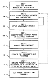
shown in the procedure flow diagram in Figure 16:
Step 1 (102): Define material under test (MITT) property
measurement requirements-define the dynamic range
and measurement tolerance requirements for the MUT
properties of interest.
Step 2 (104): Select sensor electrode geometry, configuration,
substrate material and dimensions, and source
excitation (e.g. for the periodic electrode structure in
Figure 1 select the structure, shape, and design of the
driven 34 and sensing 36 electrodes, the substrate 38,
and the conducting back plane 40 geometry).
Selection is based on test and evaluation of property
estimation sensitivity, dynamic range, and selectivity,
using the predicted responses and measurement grids
58 generated by the continuum model 60 and/or
through experimental measurements on calibrated test
pieces over the required range of properties for a
variety of electrode geometries, substrate materials,
dimensions, and configurations.
Step 3 (106): Analyze the property estimation grids and operating
point responses to define the measurement strategy-the
measurement strategy includes the number of
CA 02331644 2000-11-03
WO 99/58989 PCT/US99/10393
-20-
measurements required at different operating points
and with different sensor geometries, substrate
materials, dimensions, and configurations. A
continuum model 60 and/or set of experiments on
calibration pieces is used to generate property
estimation grids (i.e., databases) 58 and a set of
response curves which are functions of operating point
parameter variations. Operating point response curves
include (1) the standard temporal frequency or time
domain response, and responses to (2) variations in the
defined electrode geometry or for the case of periodic
structures the spatial wavelength of the sensor
electrode construct. The defined spatial wavelength.,
the wavelength of the dominant eigenfimction, or
fundamental Fourier component, in the electric scalar
potential distribution and imposed along the surface of
the MUT; the defined spatial wavelength can be
adjusted in actual measurements by including several
similar electrode constructs, each with a different
defined spatial wavelength as defined in U.S. Patent
No. 4,814,690. It can also be adjusted by use of
non-maximally symmetric sensors, such as shown in
Figure 18, together with varying the electrode pair
(e.g., NS vs. NF vs. FS pairings) used for the
measurement. (3) the relative position and kinematics
of the electrode construct to the MUT including the
height above or below the MUT surface, the position
along the surface, the orientation relative to the
surface, tilt angle and motion, and (4) adjusting the
geometry of the electrode construct (including the
distance between the driven and sensing electrodes),
CA 02331644 2000-11-03
WO 99/58989 PCT/US99/10393
-21-
the relationship between the driving and sensing
electrode widths to the wavelength ~,; the relative
position of the backplane 40 to the electrode plane;
and in the case of nonlinear, anisotropic, or
bianisotropic media the magnitude, direction, and
spatial or temporal variation of an applied DC or AC
bias electric and/or magnetic fields.
Step 4 (108): Determine useable and/or optimal operating points)
and electrode dimensions-a set of operation point
parameters, for one operating point, includes the
proximity to the MUT, the temporal frequency, and all
other adjustable parameters described in Step 3 (106).
Singular value decomposition on the Jacobian matrix,
relating variations in the transadmittance magnitude
and phase to variations in the MUT properties of
interest, is used when an accurate continuum analytical
or numerical model is available to determine the
relative performance potential at different operating
points. If such a model is not available a set of
carefully designed calibration experiments can be
used, along with models of related electrode and MCTT
geometries to provide additional insight. Relative
performance potential includes sensitivity to variations
in the MUT properties of interest, selectivity for pairs
of properties of interest, and dynamic range for each
property of interest. Then parameter estimation grids
58, also referred to as measurement grids, are
generated at optimal/selected operating points along
with operating point response curves for use in
property estimation in Step 6 (112).
CA 02331644 2000-11-03
WO 99/58989 PCT/US99/10393
-22-
Step 5 (110): Execute measurement strategy. Measure the
transadmittance at each prescribed operating point
defined in the measurement strategy, using the
admittance analyzer 44.
Step 6 ( 112): Estimate the preselected MUT properties-estimate the
MUT properties of interest, using, for example,
root-searching techniques, trial and error, table look up
and interpolation; and/or graphical interpolation from
measurement grids 58 generated with simulations, i.e.
contiliuum model, 60 and/or calibration experiments.
This is accomplished in the property estimator 46.
Step 7 (114): Estimate the property estimation tolerances-using
measurement grids 58 and operating point response
curves generated with the continuum model 60 (or
calibration experiments) and the measurement
tolerances and tolerance variations over the dynamic
range of interest for each pre-selected MUT property
of interest. If the property estimation measurement
requirements are not achieved (116), repeat Steps 2
(104) through 7 (114).
For any application, calibration experiments can be used to tune the model
parameters and improve MUT property estimation accuracy. Such calibration,
although not always required, should always be used when available.
Pronertv Estimation Grid Database and Operating Point Response Curve eneration
Each parameter estimation application will require a set of property
estimation grids, i.e., databases/measurement grids 58 and operating point
response
curves. The number of grids and response curves required will depend tin the
application. The grids and response curves have several different uses
throughout
the parameter estimation process. These uses include the following:
CA 02331644 2000-11-03
WO 99/58989 PCT/US99/10393
-23-
1) Develop a measurement strategy and select the measurement
operating points by evaluating the ML1T property estimation grids and
operating points response curves, at a variety of different operating
points over the required dynamic range for the MUT properties of
interest (Step 3 (106): of the generalized MLJT property estimation
procedure in Figure 16). Evaluating a property estimation grid
includes investigating the sensitivity, selectivity and dynamic range
for the MUT properties of interest. This is first accomplished by
visually inspecting the grids. For example, a grid which provides a
large variation iu the magnitude and phase of the transcapacitance in
response to relatively small variation in the MIJT properties of
interest would provide a good property estimation performance. This
is discussed fiwther in the next section, where the use of singular
value decomposition is described as an automated method for
identifying the "best" operating points, as well as determining the
dynamic range over which sensitivity requirements can be met for
measurement of specific MUT properties of interest.
2) Graphical estimation of the MLTT properties of interest (Step 6 (112):
of the generalized MLTT property estimation procedure in Figure 16).
For example, in Figure SA for a 2.5 mm wavelength IDED structure,
the transcapacitance and transconductance are calculated over a range
of conductivities and pennittivities, while in Figure 6 the
transcapacitances are calculated for 1 mm and 2.5 mm wavelength
)DED structures over a range of permittivities and lift-off distances.
The conductivity and permittivity for the case of Figure SA or the
permittivity and lift-off distance for the case of Figure 6 are then
estimated from each measurement for Figure 5 or pair or
measurements for Figure 6. Alternatively, the grids ar a used to obtain
first guesses for the conductivity, permittivity, or lift-off distance and
then the parameter estimated values are adjusted until the least
squares error between the measured transcapacitance and/or
CA 02331644 2000-11-03
WO 99/58989 PCT/US99/10393
-24-
transconductance and the response for the estimated permittivity,
conductivity or lift-off is minimized.
3) Determination of the estimate tolerances, as a function of the
estimated values for the MLJT properties of interest (Step 7 (114): of
the generalized MUT property estimation procedure in Figure 16).
The tolerances at a given grid point are estimated by averaging the
variation in transadmittance magnitude and phase between that grid
point and its neighboring grid points and dividing both by the average
change in magnitude and the average change in phase into the
corresponding change in the MUT property of interest. For example,
if a change in dielectric thickness of 1 mm causes a phase change of
10 degrees, the sensitivity is 1 degree per 0.1 mm If the admittance
analyzer 44 can accurately measure phase to 0.1 degrees then a 0.1
degree change in transadmittance phase would correspond to a 0.01
mm change in thickness. In other words, the limit on the
measurement precision for dielectric thickness for this example
would be 0.01 mm (the actual tolerances will vary significantly with
operatilig point specifications, MUT properties, and electrode
construct, geometry, and dimensions). Also, the value of the
measurement tolerance will vary with the MUT property estimate
value over the dynamic range for the MUT properties of interest. The
reported measurement tolerance should also include the effects of
other inherent errors due to unmodelled dynamics. These errors
could be determined for each sensor and model, using calibration test
pieces.
4) Provide comparison and evaluation of measurement strategy options.
All too often measurements are performed with inadequate
understanding of whether the measurement strategy (a.k.a., protocol,
methodolgy} is adequate to the task, what properties the strategy has,
whether such properties of the strategy could be improved or.are
already optimal. In situations where measurements of certain kinds
CA 02331644 2000-11-03
. . . vis - c~-iI-~riWCIV~.IItIV U~ : lEi- 5- 0 : ~ 1 : 03 : 7$18E32102:3-.
+48 g9 23894.465 : ~# 8
lLll LU LU~VV 111L UN~UU l11 llLLlLlf ! 1111 ltV. IV1VV~.IULvJ 1 . UV
PC'f/L; S X9/10393 _?S_
have been needed for years, or decades, ad-boc standards and roles of
t.hwnb have often accumulated, often they arc sanctified by various
standards bodies. In the absence oCn~ea~is of evaluating and co~nhaaing
nlcasurement strategies, this is the best il~t can be expected. But in
S rncasurcmcnt domains where means of evaluating and Comparing
tncasuremeni strategies h_avc been developed, ad-hocracy has been
supplanted with objective evaluation. Tliis has occurred long since for
many sin,pla measurements, e.g., circu.it measurement of voltage or
impedance. The methods disclosed herein, and their obvious cxtension~,
now ct~lzblo the choice of dielectrornctry measurement stratagios to be made
an objective scientific bases, instead of :-ales of thumb and ad-hoc
techniques. It is the analysis of the properties of measurement grids amt
operating response carves, such as condition numbers and singular value
decompositions, when applied to comparison and selection of measurement
15' strategics acid the details that compri:~e suelz strategies, that enables
ot~jeclive comparisons and rational choices.
rigvre 17 p~bvides a flow diagram describing the generation of a praperiy
estimation grid or measurement grid SR, using an analytical or numerical
continuum
model G0. Tttc same concepts described in this figure apply to the generation
of
operating point response curves. The only difference is that for property
estimation
grids the main loop is repeated for different MUT property pairs (e.g.
pcnniitivity
and conductivity, petmiilivity and lift-off or conductivity and lift-off),
while for 111e
gc;n~~raiion of operating point response cw-ves one operating point paraanctcr
is
varied over a range of intenrst (i,e. an operating point response curve is
generated by
2S computing the transadmiitance response for each incremented value of one
operating
point para,m~ter, with all other operating point parameters held constant). An
operatinb point response curve is generally a one-dilncnsional grid, where the
variable is an actjustablc opcratisig pc~i:tt parameter (e.g., lift-off,
frequency, or
wavelength) instead of a preselected MU'f properly (rive-dimensional gl3ds
that
3(1 permit properties to vary, c.g., lift-off and wavelength, are also
valuable}. The air
CA 02331644 2000-11-03 FENDED SHEE>'-
WO 99/58989 PCTNS99/10393
-26-
gap lift-off height is generally considered an operating point parameter.
However, in
many applications it is more convenient to consider the lift-off eight as a
MUT
property of interest.
Fringing Field Multi-Penetration Depth Dielectrometrv Sensor with Common
Lift-Off Height
The property estimators with multi-penetration depth dielectrornetry sensors
can be most accurate if the lift-off height for each electrode configuration
is the
same. This can be achieved with a three electrode fringing field
dielectrometry
sensor 120 shown in Figure 18A. Each set of finer electrodes 122, 124, and 126
can
be used sequentially as drive, sense, and guard electrodes. Even though the
fundamental spatial wavelength of each configuration is the same, the relative
amplitudes of each of the spatial harmonics will change with each
configuration. To
maximize the difference in harmonic amplitudes and thereby maximally change
the
effective penetration depths of the electric field, it is best to maximize the
distances
from the center electrode to the electrodes on either side. One way to
calculate this
optimum spacing is to use a "golden section". If the sensing electrode is in
the
center (such as 124 in Figure 18A), donate the electrode on one side (such as
126 in
Figure 18A) a distance x away as "far" and the electrode on the opposite side
(such
as 122 in Figure 18A) a distance a-x as "near", so that the distance from
"far" to
"near" electrodes is a, then a "golden section" is defined such that x is the
geometric
mean of a and a-x, x=[a(a-x)]1~ so that x=a(JS-I)/2 ~0.618a. With this "golden
section", the ratio of distance of "far" to "sense" (FS) electrodes to "sense"
to "near"
(NS) electrodes equals the distance ratio of "far" to "near" (FN) electrodes
to "far" to
"sense" (FS) electrodes, the ratio being ~ 1.618.
The configuration of Figure 18A is significantly different than those
proposed in the prior art. U.S. Patent 4,814,690 by Melcher et al. discloses
switching the individual elements of the interdigitated structure between
driven and
sensing to vary the fundamental wavelength of the measurement, this requires a
switch for every element in the sensor, while the configuration of Figure 18
only
requires switches to be placed at the terminals. The configuration of Figures
18A
CA 02331644 2000-11-03
.~... . . ..~~ . ~. r.-Ln: c~w.nc.,v v.s : ~ti- b- U : '? 1 : 0<3 :
7818Ei21029-~ T~9 89 23593~1Ei5 = # 9
ILLI LV LVVV t l1l UJ~UU I11 llLr_lSIl1 l 1111 11V' IU1VVLLVLV l . VV
PC'ffUSJ9I10393 -27-
~tnd 1$13 switches the roles of the drive, sense, and guard electrodes to
intentionally
vrary the penetration depths of the electric field. A switching device I3p
connects the
si:nsor 12? to the admittance anal~rier 44.
The sensor topology of higure 1$A was used with electrode widths of 500
pm; i'N centerline distance of 2470 p.rl, NS centerline distance of 1530 p,m,
and
thm a FS centerline distance 4000 pm; substrate Ihiclcncss oP254 llm;
electrode
thickness of 27 lcn~, substrate relative pcrmittivity of?.2; and a relative
hecmitt;vity
of an adjacenC dielectric of 3,0. rigure 19 shows the calculated capacit~ncc
variation
mith air-g~ li ft-off height for cacti possible pair of electrodes (NS, FS,
Fly. To
conyarc the variations for each ofthe electrode configurations it is
convenient Lo
normalize the capacitances to the difference of capacities at zero lii~i-off
(no air-gap)
to infinite life-off height (alt air-gap} as shown in Figure 20. The effective
penetration depth can be defined as that lift-off height when the capacitance
reached
97'% if its infiliite Iift-off height value, as shown by the 97% line in
Figure 20, t1s
scc;u in figure 20 t'he e~'ecEive penetration depths arc then 57p yn (NS),
1180 ~m
(fN), and 2020 ~m (1'S).
Figure 21 shows the calculated grid for a loss-free dielectric for an 8 mm
wavelength scasor with the dimensions of the previously described desisn. The
grid
shows how from measurements oftho "FS" and "r~1S" capacitances, the air-gap
tin-off height in um and dielectric permittivity can be determined. For
example, if
the measured near to sense capacitance is lZ PF and the measured far to setae
caPacitmce is 1.4 pF, then plotting the measured value on the grid of higure
21 and
interpolating along tile grid lines gives property estimates of 35 lttn for
the Iift-off
and 3.8 fc~r the relative permittivity.
ENDED SH=ET
CA 02331644 2000-11-03