Note: Descriptions are shown in the official language in which they were submitted.
CA 02331695 2000-11-03
WO 99/59127 PCT/US99/10115
METHOD FOR MODULATING A MULTIPLEXED PIXEL DISPLAY
BACKGROUND OF THE INVENTION
Field of the Invention
This invention relates generally to electronic driver circuits, and more
particularly to a
novel circuit and method for driving a display by multiplexing predetermined
voltages to
achieve modulation between saturation and threshold voltages of pixel
electrodes in a liquid
crystal display.
Description of the Background Art
FIG. 1 shows a single pixel cell 100 of a typical liquid crystal display.
Pixel cell 100
includes a liquid crystal layer 102, contained between a transparent common
electrode 104
and a pixel storage electrode 106, and a storage element 108. Storage element
108 includes
complementary data input terminals 110 and 112, data output terminal 114, and
a control
terminal 116. Responsive to a write signal on control terminal 116, storage
element 108
reads complementary data signals asserted on a pair of bit lines (B+ and B-)
118 and 120, and
latches the signal on output terminal 114 and coupled pixel electrode 106.
Liquid crystal layer 102 rotates the polarization of light passing through it,
the degree
of rotation depending on the root-mean-square (RMS) voltage across liquid
crystal layer 102.
The ability to rotate the polarization is exploited to modulate the intensity
of reflected light as
follows. An incident light beam 122 is polarized by polarizer 124. The
polarized beam then
passes through liquid crystal layer 102, is reflected off of pixel electrode
106, and passes
again through liquid crystal layer 102. During this double pass through liquid
crystal layer
102, the beam's polarization is rotated by an amount which depends on the data
signal being
asserted on pixel storage electrode 106. The beam then passes through
polarizer 126, which
passes only that portion of the beam having a specified polarity. Thus, the
intensity of the
reflected beam passing through polarizer 126 depends on the amount of
polarization rotation
induced by liquid crystal layer 102, which in turn depends on the data signal
being asserted on
pixel storage electrode 106.
1
CA 02331695 2000-11-03
WO 99/59127 PCT/US99/10115
Storage element 108 can be either an analog storage element (e.g.
capacitative) or a
digital storage element (e.g., SRAM latch). In the case of a digital storage
element, a
common way to drive pixel storage electrode 106 is via pulse-width-modulation
(PWM). In
PWM, different gray scale levels are represented by multi-bit words (i.e.,
binary numbers).
The multi-bit words are converted to a series of pulses, whose time-averaged
root-mean-
square (RMS) voltage corresponds to the analog voltage necessary to attain the
desired gray
scale value.
For example, in a 4-bit PWM scheme, the frame time (time in which a gray scale
value is written to every pixel) is divided into 15 time intervals. During
each interval, a
signal (high, e.g., 5V or low, e.g., OV) is asserted on the pixel storage
electrode 106. There
are, therefore, 16 (0-15) different gray scale values possible, depending on
the number of
"high" pulses asserted during the frame time. The assertion of 0 high pulses
corresponds to a
gray scale value of 0 (RMS OV), whereas the assertion of 15 high pulses
corresponds to a gray
scale value of 15 (RMS 5V). Intermediate numbers of high pulses correspond to
intermediate
gray scale levels.
FIG. 2 shows a series of pulses corresponding to the 4-bit gray scale value
(1010),
where the most significant bit is the far left bit. In this example of binary-
weighted pulse-
width modulation, the pulses are grouped to correspond to the bits of the
binary gray scale
value. Specifically, the first group B3 includes 8 intervals (23), and
corresponds to the most
significant bit of the value (1010). Similarly, group B2 includes 4 intervals
(22)
corresponding to the next most significant bit, group B 1 includes 2 intervals
(2 1)
corresponding to the next most significant bit, and group BO includes 1
interval (2 )
corresponding to the least significant bit. This grouping reduces the number
of pulses
required from 15 to 4, one for each bit of the binary gray scale value, with
the width of each
pulse corresponding to the significance of its associated bit. Thus, for the
value (1010), the
first pulse B3 (8 intervals wide) is high, the second pulse B2 (4 intervals
wide) is low), the
third pulse B1 (2 intervals wide) is high, and the last pulse BO (1 interval
wide) is low. This
series of pulses results in an RMS voltage that is approximately 3(10 of 15
intervals) of
the full value (5V), or approximately 4.1 V.
2
CA 02331695 2000-11-03
WO 99/59127 PCT/US99/10115
The resolution of the gray scale can be improved by adding additional bits to
the
binary gray scale value. For example, if 8 bits are used, the frame time is
divided into 255
intervals, providing 256 possible gray scale values. In general, for (n) bits,
the frame time is
divided into. (2 - 1) intervals, yielding (2') possible gray scale values.
Because the liquid crystal cells are susceptible to deterioration due to ionic
migration
resulting from a DC voltage being applied across them, the above described PWM
scheme is
modified as shown in FIG. 3. The frame time is divided in half. During the
first half, the
PWM data is asserted on the pixel storage electrode, while the common
electrode is held low.
During the second half of the frame time, the complement of the PWM data is
asserted on the
pixel storage electrode, while the common electrode is held high. This results
in a net DC
component of OV, avoiding deterioration of the liquid crystal cell, without
changing the RMS
voltage across the cell, as is well known to those skilled in the art.
FIG. 4 shows a response curve of an electrically controlled, birefringent
liquid crystal
cell. The vertical axis 402 indicates the percent of full brightness (i.e.,
maximum light
reflection) of the cell, and the horizontal axis 404 indicates the RMS voltage
across the cell.
As shown, the minimum brightness (a dark pixel) is achieved at an RMS voltage
Vtt. For
some wavelengths of light, an RMS voltage less than Vtt results in a pixel
that is not
completely dark, as shown in FIG. 4. For other wavelengths all RMS voltages
less than Vtt
result in a dark pixel. In the portion of the curve between Vtt and Vsat, the
percent brightness
increases as the RMS voltage increases, until 100% full brightness is reached
at Vsat. Once
the RMS voltage exceeds Vsat, however, the percent brightness decreases as the
RMS voltage
increases.
FIG. 5 shows an RMS voltage versus gray scale value curve, for an 8-bit (256
gray
scale values) gray scale system. The RMS voltage for each gray scale value
("Gray Value") is
given by the following formula, where Von is the digital "on" value, typically
Vdd:
Vrms = (1 / 255)(GrayValue)(Von)2
Gray scale value (x) corresponds to an RMS voltage equal to Vtt and, referring
back
to FIG. 4, to 0% brightness (i.e., minimum brightness which may not achieve
exactly 0
brightness). Thus, the gray scale values less than value (x) are unusable,
because for some
wavelengths of light, they result in a brighter rather than a darker pixel,
and for other
wavelengths, the values result in 0% brightness and are, therefore, redundant.
Similarly,
3
CA 02331695 2000-11-03
WO 99/59127 PCT/US99/10115
value (y) corresponds to an RMS voltage equal to Vsat and, referring back to
FIG. 4, to 100%
full brightness. Thus, the gray scale values greater than value (y) are also
unusable, because
they result in a darker rather than a brighter pixel. The result of these
wasted values is that
true 8-bit gray scale resolution is not obtained.
In order to avoid gray scale distortions, all gray scale values must be
confined to the
useful portion of the liquid crystal response curve (FIG. 4) between Vtt and
Vsat. One way to
accomplish this is to add an additional bit to the gray scale code (e.g., use
a 9-bit gray scale
system) and then map the 8-bit values to the values of the 9-bit system
corresponding to the
useful portion of the response curve. The addition of a single bit, however,
increases the
bandwidth requirements of the data interface by 100%, and is, therefore,
undesirable. What is
needed is a system and method for confining all of the available gray scale
values to the
useful portion of the liquid crystal response curve.
In addition to the problem of confuiing all of the grayscale values to the
useful portion
of the liquid crystal response curve, it is also difficult to implement the
debiasing (i.e.,
maintaining a net D.C. bias of OV across the pixel cells). For example, the
voltage being
asserted on the common electrode cannot be changed while data is being
asserted on the pixel
electrodes. To do so, would change the data being asserted on the display
(converting high
signals to low signals and vice versa) and distort the displayed image.
Further, because of the
substantial amount of time required to write data to the display, it is
difficult to rapidly write
an "on" state or an "off' state to the entire display. Additionally, in order
to invert the data in
the display, the complement of the data must be written to each pixel of the
display.
What is needed is a display capable of rapidly inverting the stored data,
rapidly
implementing on and off states, and providing write time flexibility.
SUMMARY
Novel methods for driving a novel display are described. In an exemplary
embodiment of the
display, each pixel cell includes a multiplexer for selectively coupling the
pixel electrode to
one of two global voltage supply terminals, responsive to a data bits stored
in the pixel cell.
This configuration provides many advantages over prior art displays which
assert the stored
data bits directly onto the pixel electrode. For example, in the present
invention, the pixel
electrodes can be digitally driven with voltages higher or lower than the
voltages used to drive
4
CA 02331695 2000-11-03
WO 99/59127 PCT/US99/10115
the logic circuitry of the display, thus providing flexibility with respect to
the time periods
that particular bits must be written to the pixel. Additionally, off states
(i.e., no voltage
across a pixel cell) can be written to all of the pixels of the display at one
time, without
changing any of the data stored in the pixel cells, by asserting appropriate
voltages on the
global voltage supply terminals and a common electrode overlaying the entire
pixel array.
Yet another advantage provided by the present invention is that the pixel
cells can be
debiased without the extra step of loading complementary data bits into the
display, simply by
asserting various predetermined voltages on the global voltage supply
terminals.
The methods of the present invention may be implemented with a voltage
controller
for asserting various predetermined voltages on the voltage supply terminals
under the control
of a processing unit executing code embodied in a computer readable medium
(e.g., a RAM
or a ROM).
According to one method of the present invention, the voltage controller
asserts a
reference voltage on the common electrode of the display, asserts the
saturation voltage of the
display on one of the voltage supply terminals, and asserts the threshold
voltage of the display
on the other of the voltage supply terminals. Then, each bit of a multi-bit
data word is
sequentially written to the pixel cells of the display, allowing each bit to
remain in the pixel
cells for a period of time dependent on the significance of each bit.
An alternate method includes the steps of sequentially writing each bit of a
multi-bit
data word to storage elements of the pixel cells; and asserting, while each
bit is stored in the
storage elements, a first predetermined voltage on the first voltage supply
terminal, a second
predetermined voltage on the second voltage supply terminal, and a third
predetermined
voltage on the common electrode, all for a time dependent on the significance
of said stored
bit to modulate the cells of the display. Optionally, this method includes the
further steps of
asserting, while each bit is stored in the storage elements, a fourth
predetermined voltage on
the first voltage supply terminal, a fifth predetermined voltage on the second
voltage supply
terminal, and a sixth predetermined voltage on the common electrode, for a
time dependent
on the significance of the stored bit, in order to debias the pixel cells.
5
CA 02331695 2000-11-03
WO 99/59127 PCT/US99/10115
BRIEF DESCRIPTION OF THE DRAWINGS
The present invention is described with reference to the following figures,
wherein
like reference numbers denote substantially similar elements:
FIG. 1 shows a block diagram of a typical liquid crystal pixel cell;
FIG. 2 shows one frame of a 4-bit binary-weighted pulse-width-modulation data;
FIG. 3 shows a split frame application of the 4-bit pulse-width-modulation
data of
FIG. 2 resulting in a net DC bias of 0 volts;
FIG. 4 shows a typical liquid crystal intensity response versus RMS voltage
curve;
FIG. 5 shows an RMS voltage versus 8-bit gray scale value curve;
FIG. 6 shows a block diagram of a multi-pixel display in accordance with the
present
invention;
FIG. 7 details a single pixel cell of the display of FIG. 6;
FIG. 8 shows a block diagram of one embodiment of a voltage controller of FIG.
7;
FIG. 9 shows a timing diagram for writing a number of binary weighted data
bits to
one embodiment of the display of FIG. 6;
FIG. 10 is a flow chart summarizing a method for implementing the timing
diagram of
FIG. 9;
FIG 11 is an RMS voltage versus gray scale value curve modified in accordance
with
the present invention to confine the gray scale values to the useful range of
RMS voltages;
FIG. 12A is a voltage chart that shows a modulation scheme and debias scheme
for
use with one embodiment of the present invention;
FIG. 12B is a chart showing sample values of the voltages shown in FIG. 12A;
FIG. 13 is a block diagram of an alternate voltage controller for implementing
a
particular driving scheme in accordance with the present invention;
FIG. 14 is a timing diagram showing an implementation of the voltage scheme of
FIG.
12A;
FIG. 15 is a flow chart summarizing the method of the driving scheme of FIG.
13;
FIG. 16 is a block diagram of an alternate voltage controller for implementing
a
particular driving scheme in accordance with the present invention;
FIG. 17 is a timing diagram showing an implementation of the voltage scheme of
FIG.
12A;
6
CA 02331695 2000-11-03
WO 99/59127 PCT/US99/10115
FIG. 18 is a flow chart summarizing a method for driving the display of FIG. 6
in
accordance with the driving scheme of FIG. 17;
FIG. 19A is a voltage chart that shows a modulation scheme and debias scheme
for
use with one embodiment of the present invention;
FIG. 19B is a chart showing sample values of the voltages shown in FIG. 19A;
FIG. 20 is a block diagram of an alternate voltage controller for implementing
a
particular driving scheme in accordance with the present invention;
FIG. 21 A is a timing diagram showing an implementation of the voltage scheme
of
FIG. 19A;
FIG. 21 B is a timing diagram showing an alternate implementation of the
voltage
scheme of FIG. 19A;
FIG. 22 is a flow chart summarizing a method for driving the display of FIG.
6, in
accordance with the driving schemes of FIGs. 21 A and 21 B;
FIG. 23A is a chart showing a modulation scheme and a debias scheme for use
with
one embodiment of the present invention;
FIG. 23B is a chart showing sample values of the voltages shown in FIG. 23A;
FIG. 24 is a block diagram of an alternate voltage controller for implementing
a
particular driving scheme in accordance with the present invention;
FIG. 25 is a timing diagram showing an implementation of the voltage scheme of
FIG.
23A;
FIG. 26 is a flow chart summarizing a method for driving the display of FIG. 6
in
accordance with the driving scheme of FIG. 25;
FIG. 27 is a block diagram of an alternate voltage controller for implementing
a
particular driving scheme in accordance with the present invention;
FIG. 28 is a timing diagram showing an alternate driving scheme for use with
the
display of FIG. 6;
FIG. 29 is a flow chart summarizing a method for driving the display of FIG. 6
in
accordance with the driving scheme of FIG. 28;
FIG. 30 is a timing diagram showing an alternate driving scheme for use with
the
display of FIG. 6;
7
CA 02331695 2000-11-03
WO 99/59127 PCTIUS99/10115
FIG. 31 is a flow chart summarizing a method for driving the display of FIG. 6
in
accordance with the driving scheme of FIG. 30;
FIG. 32 is a block diagram of an alternate voltage controller for implementing
a
particular driving scheme in accordance with the present invention;
FIG. 33 is a timing diagram showing an alternate driving scheme in accordance
with
the present invention;
FIG. 34 is a block diagram of an alternate voltage controller capable of
implementing
a particular driving scheme in accordance with the present invention;
FIG. 35 is a timing diagram showing an alternate driving scheme in accordance
with
the present invention; and
FIG. 36 is an alternate voltage controller capable of operation by a single
control
signal.
DETAILED DESCRIPTION
The present invention overcomes the problems associated with the prior art, by
using
display data bits to control the multiplexing of predetermined voltages onto
pixel electrodes
of a display, as opposed to asserting the data bits directly on the pixel
electrodes. The present
invention is described with reference to particular embodiments. Numerous
specific details
are set forth (e.g., the number of data bits in a particular data word, the on
or off chip
disposition of various voltage sources, and the number of different voltage
sources necessary
to implement particular modulation/debias schemes) in order to provide a
thorough
understanding of the invention. Those skilled in the art will understand that
the invention
may be practiced apart from these specific details. In other instances, well
known details of
display driving circuits (e.g., writing data to pixel storage cells of a
display) are omitted, so as
not to unnecessarily obscure the present invention.
FIG. 6 shows a display 600 in accordance with the present invention. Display
600
includes an array of pixel cells, a voltage controller 604, a processing unit
606, a memory
device 608, and a common transparent electrode 610, which overlays the entire
array of pixel
cells. In a particular embodiment, pixel cells 602 are formed in an integrated
monolithic
silicon backplane, overlaid with a plurality of pixel mirrors 612. A typical
pixel array
includes 768 rows and 1024 columns of pixel cells. A layer of liquid crystal
material is
8
. CA 02331695 2007-03-01
interposed between pixel mirrors 612 and common transparent electrode 610,
which is
formed, for example, from Indiurri-Tin-Oxide.
Memory 608 is a computer readable medium (e.g., RAM, ROM, etc.) having code
(e.g., data and commands) embodied therein for causing processing unit 606 to
implement the
various methods and driving schemes described herein. Processing unit 606
receives the data "
and commands from memory 608, via a memory bus 614, provides internal voltage
control
signals, via voltage control bus 616, to voltage controller 604, and provides
data control (e.g.,
data into pixel array) signals via data control bus 618.
The data control aspects of processing unit 606 are not essential to a
thorough
understanding of the present invention, because the loading of data into pixel
arrays is well
known to those skilled in the art. Further, the loading of data into a liquid
crystal display
under the control of a processing unit is described in U.S. Patent No.
6,072,452.
In brief summary, rows of data bits are asserted on bit lines
118 and 120, and then assertion of a write signal on a particular one of a
plurality of word
lines 620 causes the asserted bits to be written into the pixel cells of that
particular row. In
this manner, data bits can be sequentially written to each pixel cell of the
entire display.
Responsive to control signals received from processing unit 606, via voltage
control
bus 616, voltage controller 604 provides predetermined voltages to pixel cells
602 via a first
voltage supply terminal (V 1) 622 and a second voltage supply terminal (VO)
624. Voltage
controller 604 also asserts predetermined voltages on common electrode 610,
via a common
voltage supply terminal (VC) 626. Various embodiments of voltage controller
604 will be
disclosed herein, some requiring control signals from processing unit 606, and
others not.
Those skilled in the art will understand- that the number of control signals
required in a
particular embodiment will dictate the number of lines required in voltage
control bus 616.
Those skilled in the art will also understand that voltage controller 604,
processing unit 606,
and memory 608 may be disposed on or off chip with respect to the pixel array.
FIG. 7 shows a block diagram of an exemplary pixel cell 602 of display 600 to
include
a storage latch 702 and a multiplexer 704. Latch 702 includes complementary
input terminals
706 and 708, coupled to data lines (B+) 118 and (B-) 120, respectively, an
enable tenninal
710 coupled to word line 620, and a data output termina1712. Responsive to a
write signal
9
CA 02331695 2000-11-03
WO 99/59127 PCT/US99/10115
on word line 620, latch 702 latches the data bit on output terminal 712. In
this particular
embodiment, latch 702 is a static-random-access (SRAM) latch, but those
skilled in the art
will understand that any storage element capable of receiving a data bit,
storing the bit, and
asserting the stored bit on output termina1712 may be substituted for SRAM
latch 702.
Multiplexer 704 includes a first input terminal 714 coupled to first voltage
supply
terminal (V 1) 622, a second input termina1716 coupled to second voltage
supply terminal
(VO) 624, an output terminal 718 coupled to pixel electrode 612 (a pixel
mirror in this
particular embodiment), and a control termina1720 coupled to output terminal
712 of storage
latch 702. Thus configured, multiplexer 704, responsive to the data bit
asserted on its
control terminal 720, is operative to selectively couple pixel electrode 612
with first voltage
supply terminal (V 1) 622 and second voltage supply terminal (VO) 624. For
example, if a bit
having a logical high value (e.g., digital 1 or 5 volts) is stored in latch
702, then multiplexer
704 will couple pixel electrode 612 with first voltage supply termina1622. On
the other hand,
if a bit having a logical low value (e.g., digital 0 or 0 volts) is stored in
latch 702, then
multiplexer 704 will couple pixel electrode 612 with second voltage supply
terminal (VO)
624.
The use of the data bits stored in latch 702 as a control means, as opposed to
directly
asserting the data bit on the pixel electrode (as in pixel cell 100 of FIG.
1), provides many
advantages over the prior art. For example, the pixel electrodes can be driven
with digital
voltages higher or lower than the voltages used to drive the logic circuitry
of the display, thus
shortening or lengthening the time period that a particular bit must be
asserted on the pixel
electrodes. As another example, off states (0 volts across a pixel cell) can
be asserted on the
entire display at one time without changing any of the data stored in the
latches of the display.
Similarly, the pixel cells can be debiased (see FIG. 3) without the extra step
of writing the
complement of the data to the storage latches. These and other advantages of
the present
invention will be apparent to those skilled in the art, particularly in view
of this disclosure.
FIG. 8 is a block diagram of an alternate voltage controller 800, which
requires no
control signals from processing unit 606. Voltage controller 800 includes a
saturation voltage
(Vsat) reference 802, a threshold voltage (Vtt) reference 804, and a common
voltage (VC)
reference 806. Each of the reference voltages 802, 804, and 806, may be
generated on chip,
or may simply be connection terminals for receiving the reference voltages
from an off chip
CA 02331695 2000-11-03
WO 99/59127 PCT/US99/10115
source. Regardless of the source of the reference voltages 802, 804, and 806,
the assertion of
these voltages on first voltage supply terminal 622, second voltages supply
terminal 804, and
common voltage supply terminal 626, respectively, are deemed to be within the
functional
definition of voltage controller 800.
FIG. 9 is a timing diagram showing the writing of several data bits (B0-B4) to
display
600, while voltage controller 800 asserts Vsat, Vtt, and VC on first voltage
supply terminal
622, second voltage supply terminal 624, and common voltage supply terminal,
respectively.
Note that bits (B0-B4) are binary weighted bits, as explained above with
reference to FIG. 2,
so the time period that each bit is asserted on display 600 is dependent on
the significance of
the particular bit, even though the entire duration of bit B4 is not shown,
and other bits may
be displayed following bit B4.
Additionally, writing a bit, for example bit BO, to display 600 should be
understood to
mean writing one bit of significance BO, of each of a plurality of multi-bit
data words, to each
of a plurality of the storage elements (latches) of display 600. Thus, BO
refers to the
significance of a particular bit of a multi-bit data word, and bit BO of any
particular multi-bit
data word may have either a logical high or logical low value. The diagonal
lines in the data
portion of the timing diagram of FIG. 9 indicate that it takes a finite amount
of time to write
the particular values of each bit (e.g., BO) to each storage element of
display 600.
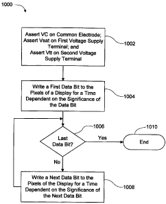
FIG. 10 is a flow chart summarizing a method 1000 for driving display 600 with
voltage controller 800 in accordance with the driving scheme shown in FIG. 9.
In a first step
1002, voltage controller 800 asserts VC, via common voltage supply
termina1626, on
common electrode 610, asserts Vsat on first voltage supply termina1622, and
asserts Vtt on
second voltage supply terminal 624. Next, in a second step 1004 a first bit
(e.g., BO) is
written to the storage elements 702 of display 600 for a time period dependent
on the
significance of the first data bit. In a next step 1006, it is determined
whether the previously
displayed bit was the last bit to be displayed. If not, then in a fourth step
1008, a next data bit
is written to the storage elements 702 of display 600 for a time period
dependent on the
significance of the next bit. Steps 1006 and 1008 are repeated until in the
third step 1006, it
is determined that the last data bit has been displayed for a time dependent
on its significance,
afterwhich, in a tenth step 1010, method 1000 ends.
11
CA 02331695 2000-11-03
WO 99/59127 PCT/US99/10115
FIG. 11 shows the results of method 1000 of multiplexing the actual saturation
voltage (Vsat) and threshold voltage (Vtt) onto the pixel electrodes of
display 600 as binary
weighted pulse-width-modulation data. In particular, the RMS voltage versus
gray scale
value curve is shifted such that a gray scale value of 0 corresponds to an RMS
voltage of Vtt
(completely dark), and a gray scale value of 255 corresponds to an RMS voltage
of Vsat (full
intensity).
Although voltage controller 800 used in conjunction with method 1000 is able
to
conform the gray scale values to the useful portion of the display response
curve, method
1000 does not, by itself, provide all of the beneficial results of the present
invention. In
particular, method 1000 does not provide for debiasing the pixel cells of
display 600 or make
allowance for the fact that data must be written to the entire display in the
relatively short
least-significant-bit (LSB) time.
FIG. 12A shows a voltage scheme which provides for both modulation and
debiasing
of display 600 in accordance with the present invention. Both the normal state
and the
inverted states contribute to the RMS modulation of the pixel cells, but the
normal and
inverted states balance each other to insure a net DC bias of 0 volts across
the cell. In the
normal state, voltage controller 604 asserts a first predetermined voltage
(VCn + Vsat) on
first voltage supply terminal (V 1) 622, a second predetermined voltage (VCn +
Vtt) on
second voltage supply terminal (VO) 624, and a third predetermined voltage
(VCn) on
common voltage supply terminal 626. In the inverted (debias) state, the
voltage controller
604 asserts a fourth predetermined voltage on the first voltage supply
terminal 622, a fifth
predetermined voltage on the second voltage supply terminal 624, and a sixth
predetermined
voltage on the common voltage supply terminal 626. In the inverted (debias)
state, the
voltage differences between the various voltage supply terminals 622, 624, and
626 must be
equal in magnitude but opposite in polarity to the respective voltage
differences in the normal
state, in order to maintain a net DC bias of 0 volts across the pixel cells of
the display.
The voltage scheme of FIG. 12A advantageously reduces the number of required
voltages on the display chip from six to four. According to this particular
scheme, the first
predetermined voltage is defined to be equal to the fifth predetermined
voltage, and the
second predetermined voltage is defined to be equal to the fourth
predetermined voltage.
Then, in order to maintain the modulation and debias conditions, all that is
required is that the
12
CA 02331695 2000-11-03
WO 99/59127 PCT/US99/10115
difference between the third predetermined voltage and the second
predetermined voltage be
equal in magnitude but opposite in polarity to the voltage difference between
the sixth
predetermined voltage and the fifth predetermined voltage. In this particular
case, the
difference between the fourth predetermined voltage and the fifth
predetermined voltage is
equal to Vtt.
FIG. 12B is a chart providing example values of voltages in accordance with
the
scheme of FIG. 12A for a liquid crystal display having a threshold voltage of
1 volt and a
saturation voltage of 3 volts. The common voltage during the normal phase
(VCn) is
arbitrarily selected to be the 0 volt reference. During the normal modulation
phase, (Vln) has
a value of 3 volts (VCn + Vsat) and (V2n) has a value of I volt (VCn + Vtt).
During the
inverted debias phase, the values of (V 1) and (VO) are interchanged such that
(V 1 i) has a
value of 1 volt and (V2i) has a value of 3 volts. In order to maintain the
required voltage
relationships, (VCi) is set at 4 volts (VOi + Vtt).
FIG. 13 is a block diagram of an alternate voltage controller 1300 capable of
implementing the voltage scheme of FIG. 12A in conjunction with display 600.
Voltage
controller 1300 includes a first voltage source 1302 for providing a (V 1)
reference voltage, a
second voltage source 1304 for providing a (VO) reference voltage, a third
voltage source
1306 for providing a normal state common (VCn) reference voltage, and a fourth
voltage
source 1308 for providing an inverted state common (VCi) reference voltage.
Although
voltage source 1306 appears three times in FIG. 13, it is actually a single
voltage source
which is shown repeatedly for the sake of clarity. Each of voltage sources
1302, 1304, 1306,
and 1308 may be on chip voltage generators, or may simply be contact terminals
for receiving
the respective voltages from an external source.
Voltage controller 1300 further includes a first multiplexer 1310, a second
multiplexer
1312, and a third multiplexer 1314. First multiplexer 1310 has a first input
terminal 1316
coupled to VCn voltage source 1306, a second input terminal 1318 coupled to
VCi voltage
source 1308, an output terminal 1320 coupled to common voltage supply terminal
626, and a
control terminal 1322 coupled to a common electrode control line 1324 of
voltage control bus
616. Second multiplexer 1312 has a first input terminal 1326 coupled to V 1
voltage source
1302, a second input terminal 1328 coupled to VCn voltage source 1306, an
output terminal
1330 coupled to first voltage supply terminal 622, and a control terminal 1332
coupled to a
13
CA 02331695 2000-11-03
WO 99/59127 PCT/US99/10115
V 1 control line 1334 of voltage control bus 616. Third multiplexer 1314 has a
first input
terminal 1336 coupled to VO voltage source 1304, a second input terminal 1338
coupled to
VCn voltage source 1306, an output terminal 1340 coupled to second voltage
supply terminal
624, and a control terminal 1342 coupled to a VO control line 1344 of voltage
control bus
616.
Voltage controller 1300 operates under the control of processing unit 606
(FIG. 6) as
follows. Responsive to a control signal received via VC control line 1324,
multiplexer 1310
selectively asserts one of reference voltages VCn or VCi onto common voltage
supply
terminal 626 and, therefore, common electrode 610. Similarly, responsive to a
control signal
received via V 1 control line 1334, multiplexer 1312 selectively asserts one
of reference
voltages V i or VCn onto first voltage supply terminal 622, and thus onto the
pixel electrodes
612 of all pixel cells 602 of display 600 currently storing a particular
digital value (e.g.,
logical high) in their respective latches 702. Additionally, responsive to a
control signal
received via VO control line 1344, multiplexer 1314 selectively asserts one of
reference
voltages VO or VCn onto second voltage supply terminal 624, and thus onto the
pixel
electrodes 612 of all pixel cells 602 of display 600 currently storing another
digital value
(e.g., logical low) in their respective latches 702.
The ability to assert predetermined voltages, via voltage supply terminals 622
and
624, onto the pixel electrodes 612 of display 600 while the data stored in the
display remains
unchanged provides great flexibility in driving display 600. Additionally, by
simultaheously
asserting the same voltage (e.g., VCn) on each of voltage supply terminals
622, 624, and 626,
voltage controller 1300 can rapidly assert an off state on every pixel cell of
display 600
without affecting the data contained therein.
FIG. 14 is a timing diagram showing how the voltage scheme of FIG. 12 may be
implemented in display 600 with voltage controller 1300. Initially, voltage
controller 1300
asserts an off state on display 600 by simultaneously asserting a same voltage
(VCn) on first
voltage supply terminal 622, second voltage supply terminal 624, and common
voltage supply
terminal 626. While the off state is being asserted on display 600, bits BO
are written to the
storage latches 702 of each pixel cell 602. Then, at a time T1, voltage
controller 1300 asserts
reference voltage V 1 on first voltage supply terminal 622 and reference
voltage VO on second
voltage supply terminal 624, each for a modulation time period dependent on
the significance
14
CA 02331695 2000-11-03
WO 99/59127 PCT/US99/10115
of bit BO. Immediately thereafter, voltage controller 1300 asserts another off
state on display
600, during which time the complements of bits BO are written to the latches
602 of display
600. Next, at a time T2, voltage controller 1300 asserts reference voltage V 1
on first voltage
supply termina1622, reference voltage VO on second voltage supply termina1624,
and
reference voltage VCi on common voltage supply terminal 626 for a time period
equal to the
modulation time period.
The loading of the complementary bits into display 600 and the reassertion of
reference voltages V1, VO, and VCi on the respective voltage supply terminals
debiases the
pixel cells as follows. First, replacing each bit in display 600 with its
complement effectively
interchanges reference voltage V 1 with reference voltage VO, as described
with respect to
FIG. 12A. Second, reference voltage VCi is selected such that the voltage
difference between
VCn and VO is equal in magnitude but opposite in polarity to the voltage
difference between
VCi and V 1. Therefore, the voltage across a pixel cell storing a particular
bit is equal in
magnitude but opposite in polarity to the voltage across the pixel cell when
storing the
complement of the bit. It is important to note that the debiasing step also
contributes to the
RMS voltage generated across each pixel cell, and must therefore be considered
when
determining the appropriate time interval for a bit of a particular
significance.
Voltage controller asserts another off state on display 600 while bit B 1 is
written to
display 600. Then, at a time T3, voltage controller 1300 asserts reference
voltage V 1 on first
voltage supply terminal 622 and reference voltage VO on second voltage supply
terminal 624,
all for a second modulation time period dependent on the significance of bit B
1. Immediately
thereafter, voltage controller 1300 asserts another off state on display 600,
during which time
the complements of bits B1 are written to display 600. Then, at a time T4,
voltage controller
1300 asserts reference voltage V 1 on first voltage supply terminal 622,
reference voltage VO
on second voltage supply termina1624, and reference voltage VCi on common
voltage supply
terminal 626 for a time period equal to the second modulation time period. The
remaining
data bits and their complements are written to display 600, and the reference
voltages are
asserted on their respective voltage supply terminals for periods of time
depending on their
respective significance, as described above with respect to bits BO and B 1.
FIG. 15 is a flow chart summarizing a method 1500 for driving a display in
accordance with the voltage scheme of FIG. 12A. In a first step 1502, voltage
controller 1300
CA 02331695 2000-11-03
WO 99/59127 PCT/US99/10115
asserts an off state (a same voltage) to first voltage supply terminal 622, to
second voltage
supply terminal 624, and common electrode 610. Next, in a second step 1504, a
first data bit
is written to pixel cells 602 of display 600. Then, in a third step 1506,
voltage controller
1300 asserts a first predetermined voltage on first voltage supply terminal
622, a second
predetermined voltage on second voltage supply terminal 624, and a third
predetermined
voltage on common electrode 610, all for a time dependent on the significance
of the first
data bit. In a fourth step 1508, voltage controller 1300 asserts an off state
to display 600, and
then in a fifth step 1510, the complement of the first data bit is written to
pixel cells 602 of
display 600. Next, in a sixth step, voltage controller 1300 asserts the first
predetermined
voltage on second voltage supply terminal 624, asserts the second
predetermined voltage on
first voltage supply termina1622, and asserts a fourth predetermined voltage
on common
electrode 610, all for a time period dependent on the significance of the
stored data bit. In a
seventh step 1514, if the last data bit has not been written to display 600,
then in an eighth
step 1516, a next data bit is written to the pixels of the display, and method
1500 returns to
third step 1506. If, however, in seventh step 1514, it is determined that the
last data bit has
been written to display 600, then in a ninth step 1518 method 1500 ends.
FIG. 16 is a block diagram of an alternate voltage controller 1600 capable of
implementing the voltage scheme of FIG. 12A in conjunction with display 600,
without the
need to write complementary data bits to display 600. Voltage controller 1600
includes a first
voltage source 1602 for providing a (V 1 n) reference voltage, a second
voltage source 1604
for providing a (V 1 i) reference voltage, a third voltage source 1606 for
providing a nonmal
state common (VCn) reference voltage, and a fourth voltage source 1608 for
providing an
inverted state common (VCi) reference voltage. Although voltage source (V 1 i)
1604 appears
twice in FIG. 16, it is actually a single voltage source which is shown
repeatedly for the sake
of clarity. Similarly, voltage source (V 1 n) 1602, shown three times, is also
a single voltage
source. Additionally, because voltage (V 1 i) is equal to voltage (VOn), and
voltage (V 1 n) is
equal to voltage (VOi) according to the voltage scheme of FIG. 12A, it is not
necessary to
show separate voltage sources for voltages (VOn) and (VOi). Each of voltage
sources 1602,
1604, 1606, and 1608 may be on chip voltage generators, or may simply be
contact terminals
for receiving the respective voltages from an external source.
16
CA 02331695 2000-11-03
WO 99/59127 PCT/US99/10115
Voltage controller 1600 further includes a first multiplexer 1610, a second
multiplexer
1612, and a third multiplexer 1614. First multiplexer 1610 has a first input
terminal coupled
to VCn voltage source 1606, a second input terminal coupled to VCi voltage
source 1608, a
third input terminal coupled to V 1 n voltage source 1602, an output terminal
coupled to
common voltage supply terminal 626, and a 2-bit control terminal set coupled
to a 2-bit
common electrode control line 1616 of voltage control bus 616. Second
multiplexer 1612 has
a first input terminal coupled to V 1 n voltage source 1602, a second input
terminal coupled to
V 1 i voltage source 1604, an output terminal coupled to first voltage supply
terminal 622, and
a control terminal coupled to a V 1 control line 1618 of voltage control bus
616. Third
multiplexer 1614 has a first input terminal coupled to V 1 i voltage source
1604, a second
input terminal coupled to V 1 n voltage source 1602, an output terminal
coupled to second
voltage supply terminal 624, and a control terminal coupled to a VO control
line 1620 of
voltage control bus 616.
Voltage controller 1600 operates under the control of processing unit 606
(FIG. 6) as
follows. Responsive to a control signal received via 2-bit VC control line
1616, multiplexer
1610 selectively asserts one of reference voltages VCn, VCi, or V 1 i onto
common voltage
supply terminal 626 and, therefore, common electrode 610. Similarly,
responsive to a control
signal received via V i control line 1618, multiplexer 1612 selectively
asserts one of reference
voltages V 1 n or V 1 i onto first voltage supply terminal 622, and thus onto
the pixel electrodes
612 of all pixel cells 602 of display 600 currently storing a particular
digital value (e.g.,
logical high) in their respective latches 702. Additionally, responsive to a
control signal
received via VO control line 1620, multiplexer 1614 selectively asserts one of
reference
voltages V 1 i or V 1 n onto second voltage supply terminal 624, and thus onto
the pixel
electrodes 612 of all pixel cells 602 of display 600 currently storing another
digital value
(e.g., logical low) in their respective latches 702. Voltage controller 1600
has an advantage
over voltage controller 1300 in that voltage controller 1600 can assert both
voltages V 1 n and
V 1 i on either of voltage supply terminals 622 or 624, thus eliminating the
need to write
complementary data bits to display 600 to achieve debiasing of the pixel
cells.
FIG. 17 is a timing diagram showing an implementation of the voltage scheme of
FIG.
12A with voltage controller 1600. Initially, voltage controller 1600 asserts
an off state on
display 600 by asserting a same voltage (i.e., (V In)) on each of first
voltage supply terminal
17
CA 02331695 2000-11-03
WO 99/59127 PCT/US99/10115
622, second voltage supply terminal 624, and common voltage supply terminal
626. While
the off state is asserted on display 600, bit BO is written to display 600.
Then, at a time T1,
voltage controller 1600 asserts voltage (V 1 n) on first voltage supply
termina1622, voltage
(V 1 i) on second voltage supply termina1624, and voltage (VCn) on common
voltage supply
termina1626. Then, after a period of time dependent on the significance of the
bit (BO) stored
in display 600, voltage controller 1600 switches to debias mode, with bit BO
still stored in the
latches 702 of display 600, by asserting voltage (V i i) on first voltage
supply terminal 622,
voltage (V ln) on second voltage supply terminal 624, and voltage (VCi) on
common voltage
supply termina1626, for the same period of time dependent on the significance
of the stored
bit BO. Afterwards, at a time T2, voltage controller 1600 writes an off state
to display 600 so
that the next bit (B 1) can be written to display 600. The modulation and
debiasing of display
600 for the remaining bits occurs substantially as described for bit BO,
except that the time
periods that voltage controller 1600 asserts the various reference voltages on
the respective
voltage supply terminals varies according to the significance of the
particular bits written to
display 600.
FIG. 18 is a flow chart summarizing an alternate method 1800 for driving a
display in
accordance with the voltage scheme of FIG. 12A. In a first step 1802, voltage
controller 1600
writes an off state to display 600. Then, in a second step 1804, a first data
bit is written to
pixel cells 602 of display 600. In a third step 1806, voltage controller 1600
asserts a first
predetermined voltage (V 1 n) on first voltage supply termina1622, a second
predetermined
voltage (V 1 i) on second voltage supply terminal 624, and a third
predetermined voltage
(VCn) on common electrode 610, all for a time period dependent on the
significance of the
data bit written to display 600. Next, in a fourth step 1808, voltage
controller 1600 asserts the
first predetermined voltage (V ln) on second voltage supply termina1624, the
second
predetermined voltage (V I i) on first voltage supply terminal 622, and a
fourth predetermined
voltage on common electrode 610, all for a time period equal to the time
period dependent on
the significance of the data bit written to display 600. In a fifth step 1810,
voltage controller
1600 writes another off state to display 600. In a sixth step 1812, if the
last data bit has not
been written to display 600, then in a seventh step 1814, a next data bit is
written to display
600, and method 1800 returns to the third step 1806. If, in the sixth step
1812, the last bit had
been written to display 600, then in an eighth step 1816, method 1800 ends.
18
CA 02331695 2000-11-03
WO 99/59127 PCT/US99/10115
FIG. 19A is a chart illustrating an alternate voltage scheme for use in
accordance with
the present invention, wherein common electrode 610 is maintained at the same
voltage (VC)
during both the normal and inverted debiasing states. The voltages asserted on
first voltage
supply termina1622 and second voltage supply termina1624 are toggled about VC
in order to
modulate and debias the pixel cells of display 600. In particular, during the
normal state, a
first predetermined reference voltage (VC) is asserted on common voltage
supply terminal
(VC) 626, a second predetermined reference voltage (VC + Vsat) is asserted on
first voltage
supply terminal (Vl) 622, and a third predetermined reference voltage (VC +
Vtt) is asserted
on second voltage supply terminal (VO) 624. During the inverted (debias)
state, the first
predetermined voltage (VC) is asserted on common voltage supply terminal (VC)
626, a
fourth predetermined voltage (VC - Vsat) is asserted on first voltage supply
terminai (V 1)
622, and a fifth predetermined voltage (VC - Vtt) is asserted on second
voltage supply
terminal (VO) 624. The voltage scheme of FIG. 19A beneficially eliminates the
need to drive
the voltage on common electrode 610, but requires a greater number of voltages
(i.e., 4) to
drive first voltage supply terminal 622 and second voltage supply terminal
624.
FIG. 19B is a chart showing exemplary values for a display having a common
electrode maintained at 3 volts, a threshold voltage (Vtt) of 1 volt, and a
saturation voltage
(Vsat) of 3 volts. In this example, in the normal state, 6 volts (VC + Vsat)
is asserted on the
first voltage supply terminal, and 4 volts (VC + Vtt) is asserted on the
second voltage supply
terminal. In the inverted state 0 volts (VC - Vsat) is asserted on the first
voltage supply
terminal, and 2 volts (VC - Vtt) is asserted on the second voltage supply
terminal.
FIG. 20 is a block diagram of an alternate voltage controller 2000, capable of
implementing the voltage scheme of FIG. 19A, in conjunction with display 600
of FIG. 6.
Voltage controller 2000 includes a first voltage source 2002 for providing a
first reference
voltage (VC), a second voltage source 2004 for providing a second reference
voltage (V1n), a
third voltage source 2006 for providing a third reference voltage (VOn), a
fourth voltage
source 2008 for providing a fourth reference voltage (V i i), and a fifth
voltage source 2010 for
providing a fifth reference voltage (VOi). Although first voltage source 2002
is shown three
times in FIG. 20 for the sake of clarity, it should be understood that first
voltage source 2002
is actually a single voltage source. Additionally, it should be understood
that any or all of
voltage sources 2002, 2004, 2006, 2008, and 2010 may be either on chip voltage
generators
19
CA 02331695 2000-11-03
WO 99/59127 PCT/US99/10115
or simply supply terminals for receiving the respective reference voltages
from an off chip
source.
Voltage controller 2000 further includes a first multiplexer 2012 and a second
multiplexer 2014. Multiplexer 2012 includes a first input terminal coupled to
second voltage
source 2004, a second input terminal coupled to fourth voltage source 2008, a
third input
terminal coupled to first voltage source 2002, an output terminal coupled to
first voltage
supply terminal 622, and a 2-bit control terminal set coupled to two V 1
control lines 2012 of
voltage control bus 616. Multiplexer 2014 includes a first input terminal
coupled to third
voltage source 2006, a second input terminal coupled to fifth voltage source
2010, a third
input terminal coupled to first voltage source 2002, an output terminal
coupled to second
voltage supply terminal 624, and a 2-bit control terminal set coupled two VO
control lines
2014 of voltage control bus 616.
Voltage controller 2000 operates under the control of processing unit 606 as
follows.
First voltage source 2002 asserts reference voltage VC on common voltage
supply terminal
626. Multiplexer 2012, responsive to control signals received via V 1 control
lines 2012
selectively asserts one of reference voltages V 1n, V 1 i, or VC onto first
voltage supply
termina1622, and thus onto the pixel electrodes 612 of all pixel cells 602
currently storing a
logical high data bit. Multiplexer 2014, responsive to control signals
received via VO control
lines 2014 selectively asserts one of reference voltages VOn, VOi, or VC onto
second voltage
supply termina1624, and thus onto the pixel electrodes 612 of all pixel cells
602 currently
storing a logical low data bit.
FIG. 21 A is a timing diagram showing an implementation of the voltage scheme
of
FIG. 19A with voltage controller 2000. Initially, voltage controller 2000
asserts an off state
on display 600 by asserting a same voltage (i.e., VC) on each of first voltage
supply terminal
622, second voltage supply terminal 624, and common voltage supply
termina1626. While
the off state is asserted on display 600, bit BO is written to the latches 702
of display 600.
Then, at a time Tl, voltage controller 2000 asserts voltage (Vln) on first
voltage supply
termina1622, voltage (VOn) on second voltage supply termina1624, and maintains
voltage
(VC) on common voltage supply termina1626. Then, after a period of time
dependent on the
significance of the bit (BO) stored in display 600, voltage controller 2000
switches to the
debias state, with bit BO still stored in the latches 702 of display 600, by
asserting voltage
CA 02331695 2000-11-03
WO 99/59127 PGT/US99/10115
(V 1 i) on first voltage supply termina1622, voltage (VOi) on second voltage
supply terminal
624, and maintaining voltage (VC) on common voltage supply terminal 626, for a
time period
equal to the previous period of time dependent on the significance of the
stored bit BO.
Afterwards, at a time T2, voltage controller 2000 writes an off state to
display 600 so that the
next bit (B I) can be written to display 600. The modulation and debiasing of
display 600 for
the remaining bits occurs substantially as described for bit BO, except that
the time periods
that voltage controller 2000 asserts the various reference voltages on the
respective voltage
supply terminals varies according to the significance of the particular bits
written to display
600.
FIG. 21B is a timing diagram similar to that shown in FIG. 21A, except that no
off
states are used when writing data bits to display 600. FIG. 21 B is presented
only to illustrate
that off states are not required to properly modulate and debias a display.
For example, note
that starting at time T 1, the writing of bit B 1 to display 600 takes a
finite amount of time,
delaying the assertion of the respective voltages on the pixel cells at the
bottom of display by
bit B 1. This delay is, however, compensated for by the same delay incurred in
writing the
next bit B2 to display 600.
FIG. 22 is a flow chart summarizing an alternate method 2200 for driving a
display in
accordance with the voltage scheme of FIG. 19A. In a first step 2202, voltage
controller 2000
writes an off state to display 600. Then, in a second step 2204, a first data
bit is written to
pixel cells 602 of display 600. Next, in a third step 2206, voltage controller
2000 asserts a
first predetermined voltage on conunon electrode 610, and in a fourth step
2208 asserts a
second predetermined voltage on first voltage supply terminal 622 and a third
predetermined
voltage on second voltage supply terminal 624, both for a time period
dependent on the
significance of the data bits written to the pixel cells 602 of display 600.
Then, in a fifth step
2210, voltage controller 2000 asserts a fourth predetermined voltage on first
voltage supply
terminal 622 and a fifth predetermined voltage on second voltage supply
terminal 624, both
for a time period equal to the time period dependent on the significance of
the data bits
written to the pixel cells 602 of display 600. Next, in a sixth step 2212,
voltage controller
2000 writes an off state to display 600. In a seventh step 2214, it is
determined whether the
last data bit has been written to display 600, and if not, then in an eighth
step 2216, a next
data bit is written to the pixel cells 602 of display 600, afterwhich method
2200 returns to
21
CA 02331695 2000-11-03
WO 99/59127 PCT/US99/10115
fourth step 2208. If, in the seventh step 2214, it was determined that the
last data bit had been
written to display 600, then in a ninth step 2218, method 2200 ends.
FIG. 23A is a chart illustrating another alternate voltage scheme for use in
accordance
with the present invention. In this particular voltage scheme, during the
normal state, a first
predetermined reference voltage (VCn) is asserted on common voltage supply
terminal (VC)
626, a second predetermined reference voltage (VCn + Vsat) is asserted on
first voltage
supply terminal (V 1) 622, and a third predetermined reference voltage (VCn +
Vtt) is asserted
on second voltage supply terminal (VO) 624. During the inverted (debias)
state, a fourth
predetermined voltage (VCi) is asserted on common voltage supply terminal (VC)
626, a fifth
predetermined voltage (VCi - Vsat) is asserted on first voltage supply
terminal (V1) 622, and
a sixth predetermined voltage (VCi - Vtt) is asserted on second voltage supply
terminal (VO)
624. The voltage scheme of FIG. 23A beneficially provides flexibility with
respect to the
particular voltage values which may be employed, but requires the greatest
number of
voltages (i.e., 6) to drive first voltage supply terminal 622, second voltage
supply terminal
624, and common voltage supply terminal 626.
FIG. 23B is a chart showing exemplary values for a display having a threshold
voltage
(Vtt) of 1 volt, and a saturation voltage (Vsat) of 3 volts. Additionally, VCn
and VCi are
arbitrarily selected to be 0 volts and 5 volts, respectively. In this example,
in the normal state,
3 volts (VCn + Vsat) is asserted on the first voltage supply terminal, and I
volt (VCn + Vtt) is
asserted on the second voltage supply terminal. In the inverted state 2 volts
(VCi - Vsat) is
asserted on the first voltage supply terminal, and 4 volts (VCi - Vtt) is
asserted on the second
voltage supply terminal.
FIG. 24 is a block diagram of an alternate voltage controller 2400, capable of
implementing the voltage scheme of FIG. 23A, in conjunction with display 600
of FIG. 6.
Voltage controller 2400 includes a first voltage source 2402 for providing a
first reference
voltage (V 1 n), a second voltage source 2404 for providing a second reference
voltage (VOn),
a third voltage source 2406 for providing a third reference voltage (VCn), a
fourth voltage
source 2408 for providing a fourth reference voltage (V 1 i), a fifth voltage
source 2410 for
providing a fifth reference voltage (VOi), and a sixth voltage source 2412 for
providing a
sixth reference voltage (VCi). Although fifth voltage source 2410 is shown
three times in
FIG. 24 for the sake of clarity, it should be understood that fifth voltage
source 2410 is
22
CA 02331695 2000-11-03
WO 99/59127 PCT/US99/10115
actually a single voltage source. Additionally, it should be understood that
any or all of
voltage sources 2402, 2404, 2406, 2408, 2410, and 2412 may be either on chip
voltage
generators or simply supply terminals for receiving the respective reference
voltages from an
off chip source.
Voltage controller 2400 further includes a first multiplexer 2414, a second
multiplexer
2416, and a third multiplexer 2018. Multiplexer 2414 includes a first input
terminal coupled
to third voltage source 2406, a second input terminal coupled to sixth voltage
source 2412, a
third input terminal coupled to fifth voltage source 2410, an output tenminal
coupled to
common voltage supply termina1626, and a 2-bit control terminal set coupled to
two VC
control lines 2420 of voltage control bus 616. Multiplexer 2416 includes a
first input
terminal coupled to first voltage source 2402, a second input tenninal coupled
to fourth
voltage source 2408, a third input terminal coupled to fifth voltage source
2410, an output
terminal coupled to first voltage supply termina1622, and a 2-bit control
terminal set coupled
two V 1 control lines 2422 of voltage control bus 616. Third multiplexer 2418
includes a first
input terminal coupled to second voltage source 2404, a second input terminal
coupled to
fifth voltage source 2410, an output terminal coupled to second voltage supply
terminal 624,
and a single control terminal coupled to a VO control line 2424 of voltage
control bus 616.
Voltage controller 2400 operates under the control of processing unit 606 as
follows.
Multiplexer 2414, responsive to control signals received via VC control lines
2420,
.20 selectively asserts on of reference voltages VCn, VCi, of VOi onto common
voltage supply
terminal 626, and thus also on common electrode 610. Multiplexer 2416,
responsive to
control signals received via V 1 control lines 2422 selectively asserts one of
reference voltages
V 1 n, V 1 i, or VOi onto first voltage supply terminal 622, and thus onto the
pixel electrodes
612 of all pixel cells 602 currently storing a logical high data bit.
Multiplexer 2418,
responsive to control signals received via VO control line 2424 selectively
asserts one of
reference voltages VOn or VOi onto second voltage supply termina1624, and thus
onto the
pixel electrodes 612 of all pixel cells 602 currently storing a logical low
data bit.
FIG. 25 is a timing diagram showing an implementation of the voltage scheme of
FIG.
23A with voltage controller 2400. Initially, voltage controller 2400 asserts
an off state on
display 600 by asserting a same voltage (i.e., VOi) on each of first voltage
supply terminal
622, second voltage supply termina1624, and common voltage supply terminal
626. While
23
CA 02331695 2000-11-03
WO 99/59127 PCT/US99/10115
the off state is asserted on display 600, bit BO is written to the latches 702
of display 600.
Then, at a time T 1, voltage controller 2400 asserts voltage (V In) on first
voltage supply
termina1622, voltage (VOn) on second voltage supply terminal 624, and voltage
(VCn) on
common voltage supply terminal 626. Then, after a period of time dependent on
the
significance of the bit (BO) stored in display 600, voltage controller 2400
switches to the
debias state, with bit BO still stored in the latches 702 of display .600, by
asserting voltage
(V 1 i) on first voltage supply terminal 622, voltage (VOi) on second voltage
supply terminal
624, and voltage (VCi) on common voltage supply termina1626, for a time period
equal to
the previous period of time dependent on the significance of the stored bit
BO. Immediately
thereafter, voltage controller 2400 reasserts an off state on display 600, by
asserting voltage
(VOi) on each of voltage supply terminals 622, 624, and 626, so that the next
bit (B 1) can be
written to display 600. The modulation and debiasing of display 600 for the
remaining bits
occurs substantially as described for bit BO, except that the time periods
that voltage
controller 2400 asserts the various reference voltages on the respective
voltage supply
terminals varies according to the significance of the particular bits written
to display 600.
FIG. 26 is a flow chart summarizing an alternate method 2600 for driving
display 600
in accordance with the voltage scheme of FIG. 23A. In a first step 2602,
voltage controller
2400 asserts an off state on display 600. Then, in a second step 2604, a first
data bit is written
to the pixel cells 602 of display 600. Next, in a third step 2606, voltage
controller 2400
asserts a first predetermined voltage on first voltage supply terminal 622, a
second
predetermined voltage on second voltage supply termina1624, and a third
predetermined
voltage on common voltage supply termina1626, all for a time period dependent
on the
significance of the bit stored in display 600. Thereafter, in a fourth step
2608, voltage
controller 2400 asserts a fourth predetermined voltage on first voltage supply
terminal 622, a
fifth predetermined voltage on second voltage supply termina1624, and a sixth
predetermined
voltage on common voltage supply termina1626, all for a time period equal to
the previous
time period dependent on the significance of the data bit stored in display
600. Next, in a
fifth step 2610, voltage controller asserts an off state on display 600. In a
sixth step 2612, it
is determined whether the last data bit has been written to display 600. If
not, then in a
seventh step 2614, a next data bit is written to pixel cells 602 of display
600, and method
24
= = , CA 02331695 2007-03-01
2600 returns to the third step 2606. If, in the sixth step 2612 it was
determined that the last
data bit had been written to display 600, then in an eighth step 2616, method
2600 ends.
The various voltage controllers described above have generally relied on
modulating
display 600 by asserting a limited number of voltages on first voltage supply
terminal 622,
second voltage supply temiinal 624, and common voltage supply terminal 626 for
periods of
time dependent on the significance of the bits stored in display 600. Because
the response of
pixel cells 602 depends on the RMS voltages across the cells, other modulation
schemes are
possible. For example, in one scheme, a pixel can be modulated by varying the
amplitude of
a voltage pulse, while holding the time duration constant. Alternatively, the
duration of the
pulse can be varied, while holding the voltage amplitude constant. In yet
another scheme,
both the amplitude and the duration of the pulse can be varied.
FIG. 27 is a block diagram of an alternate voltage controller 2700 for
implementing a
modulationldebiasing scheme based on voltage amplitudes. Voltage controller
2700 includes
a first voltage source 2702 for providing a first reference voltage (VC), a
first plurality 2704
of voltage sources for providing a variety of reference voltages for selective
assertion on first
voltage supply terminal (V 1) 622. and a second plurality of voltage sources
for providing a
variety of reference voltages for selective assertion on second voltage supply
terminal (VO)
624. Each of the voltage sources of the first plurality 2704 of voltage
sources provides a
voltage whose amplitude depends on the significance of an associated one of
data bits (BO-
B9) and the saturation voltage (Vsat) of display 600. Similarly, each of the
voltage sources of
the second plurality of voltage sources provides a voltage whose amplitude
depends on the
significance of an associated one of data bits (B0-B9) and the threshold
voltage (Vtt) of
display 600. Additionally, each of the voltage sources in the first plurality
2704 and the
second plurality 2706 of voltage sources is associated with another of the
voltage sources to
implement debiasing of the pixel cells. For example, voltage V I n(B2) is
equal in magnitude
but opposite in polarity (with respect to voltage VC) than voltage V 1 i(B2).
Note that in this particular embodiment, bits (B5-B9) are of coequal
significance (i.e_,
equally weighted). Such a data scheme is described in detail in U.S. Patent
No. 6,151,011.
CA 02331695 2000-11-03
WO 99/59127 PCT/US99/10115
Voltage controller 2700 further includes a first multiplexer 2708 and a second
multiplexer 2710. First multiplexer 2708 includes a plurality of input
terminals, each coupled
one of voltage sources of the first plurality 2704 of voltage sources, an
additional input
terminal coupled to first voltage source 2702, an output terminal coupled to
first voltage
supply terminal 622, and a 4-bit control terminal set coupled to V 1 control
lines 2712 of
voltage control bus 616. Responsive to control signals received from
processing unit 606, via
V 1 control lines 2712, multiplexer 2708 selectively asserts one of the
reference voltages
coupled to its input terminals onto first voltage supply terminal 622. Second
multiplexer
2710 includes a plurality of input terminals, each coupled to one of voltage
sources of the first
plurality 2706 of voltage sources, an additional input terminal coupled to
first voltage source
2702, an output terminal coupled to second voltage supply terminal 624, and a
4-bit control
terminal set coupled to VO control lines 2714 of voltage control bus 616.
Responsive to
control signals received from processing unit 606, via VO control lines 2714,
multiplexer
2710 selectively asserts one of the reference voltages coupled to its input
terminals onto
second voltage supply terminal 624.
Although first voltage source 2702 is shown three times in FIG. 27 for the
sake of
clarity, it should be understood that first voltage source 2702 is actually a
single device.
Additionally, any or all of the voltage sources shown in FIG. 27 may be on-
chip voltage
generators or, alternatively, simply supply terminals for receiving the
various voltages from
an off chip source.
FIG. 28 is a timing diagram showing a particular scheme for modulating and
debiasing display 600 (FIG. 6) with voltage controller 2700 of FIG. 27.
Initially, voltage
controller 2700 asserts an off state on display 600, while bit BO is written
to pixel cells 602.
Then, at a time T 1, voltage controller 2700 asserts reference voltage V 1
n(B0) on first voltage
supply termina1622, reference voltage VOn(B0) on second voltage supply
terminal 624, and
reference voltage VC on common voltage supply terminal 626, all for a time
period having a
predetermined duration Tk. Immediately thereafter, voltage controller 2700
asserts reference
voltage V 1 i(B0) on first voltage supply terminal 622, reference voltage
VOi(B0) on second
voltage supply termina1624, and reference voltage VC on common voltage supply
terminal
626, all for time Tk. Next, voltage controller 2700 asserts another off state
on display 600,
during which bit B1 is written to pixel cells 602 of display 600. Then, at
time T2, with bit B1
26
CA 02331695 2000-11-03
WO 99/59127 PCT/US99/10115
stored in latches 702 of display 600, voltage controller 2700 asserts voltage
V 1 n(B 1) on first
voltage supply terminal 622, voltage VOn(B 1) on second voltage supply
terminal 624, and
voltage VC on common voltage supply termina1624, all for time Tk. Immediately
thereafter,
in order to debias the pixel cells, voltage controller 2700 asserts voltage V
1 i(B 1) on first
voltage supply terminal 622, voltage VOi(B 1) on second voltage supply
terminal 624, and
voltage VC on common voltage supply termina1624.
Subsequent bits (B2-B4) are written to display 600, and their associated
voltages are
asserted on first voltage supply terminal 622 and second voltage supply
termina1624 for time
Tk. The voltage pulses for bits B5-B9 are shown broken, because the page is
not large
enough to show the amplitude of voltages V 1 n(B5-B9) and V 1 i(B5-B9) in
proper scale. In
every case, however, the time width of the respective pulse is the same (Tk),
and the
amplitude of the reference voltages are selected to generate an RMS voltage
appropriate for
the significance of the associated bit.
FIG. 29 is a flow chart summarizing a method 2900 for writing a multi-bit data
word
to display 600 in accordance with an amplitude based voltage scheme such as
that described
with reference to FIG. 28. In a first step 2902, voltage controller 2700
writes an off state to
display 600. Then, in a second step 2904, a first data bit (e.g., BO) is
written to the pixels of
display 600. Next, in a third step 2906, voltage controller 2700 asserts a
first predetermined
voltage (VC), via common voltage supply terminal 626, onto common electrode
610. Then,
in a fourth step 2908, voltage controller 2700 asserts a second predetermined
voltage (e.g.,
V ln(B0)) on first voltage supply terminal 622, and a third predetermined
voltage (e.g.,
VOn(B0)) on second voltage supply terminal 624, both for a first predetermined
time period,
and each having an amplitude dependent on the significance of the bit in
display 600. Next,
in a fifth step 2910, voltage controller 2700 asserts a fourth predetermined
voltage (e.g.,
V 1 i(B0) on first voltage supply terminal 622, and a fifth predetermined
voltage (e.g.,
VOi(B0)) on second voltage supply terminal 624, both for a second
predetermined time
period, and each having an amplitude dependent on the significance of the data
bit in display
600. In a particular method, the first predetermined time period is equal to
the second
predetermined time period, the second predetermined voltage is equal in
amplitude but
opposite in polarity to the fourth predetermined voltage, and the third
predetermined voltage
is equal in magnitude but opposite in polarity to the fifth predetermined
voltage. In any
27
CA 02331695 2000-11-03
WO 99/59127 PCT/US99/10115
event, the assertion of the various predetermined voltages for their
respective time periods
combine to result in a net DC bias of 0 volts across the pixel cells 602 of
display 600. Next,
in a sixth step 2912, voltage controller 2700 asserts an off state on display
600. In a seventh
step 2914, it is determined whether the last data bit has been written to
display 600. If not,
then in an eighth step 2916, a next data bit (e.g., B 1) is written to the
storage elements 702 of
display 600, and method 2900 retums to fourth step 2908. If, however, in the
seventh step
2914, it is determined that the last data bit (e.g., B9) has been written to
the latches 702 of
display 600, then in a ninth step 2918, method 2900 ends.
FIG. 30 is a timing diagram that shows a scheme for writing multi-bit data
words to
display 600, which utilizes both time and amplitude modulation to generate
desired RMS
voltages. In other words, the time period that a particular voltage is
asserted on a voltage
supply line depends on both the amplitude of the asserted voltage and the
significance of the
bit stored in the latches 702 of display 600. Such a driving scheme can be
carried out with a
voltage controller having fewer voltage sources than voltage controller 2700.
To illustrate,
the timing diagram of FIG. 30 will be described with reference to voltage
controller 2700, but
noting that not all voltage sources of voltage controller 2700 are utilized.
Initially, voltage controller 2700 asserts an off state (voltage VC on first
voltage
supply termina1622, second voltage supply terminal 624, and common voltage
supply
terminal 626) on display 600, during which time bit BO is written to storage
elements 702 of
display 600. Then, at time TI, voltage controller 2700 asserts voltage V
ln(B0) 3002 on first
voltage supply terminal (V1) 622, and asserts voltage VOn(B0) 3004 on second
voltage
supply terminal (VO) 624, both for a period of time (x). Immediately
thereafter, voltage
controller 2700 asserts voltage V 1 i(B0) 3006 on first voltage supply
terminal (V 1) 622, and
asserts voltage VOi(B0) 3008 on second voltage supply terminal (VO) 624, both
for an equal
period of time (x). Immediately thereafter, voltage controller 2700 asserts a
second of state
on display 600, during which the next bit B1 is written to storage elements
702 of display
600.
Next, rather than asserting voltage V 1 n(B 1) and VOn(B 1) on first voltage
supply
terminal 622 and second voltage supply terminal 624, respectively, voltage
controller 2700
reasserts voltage V ln(B0) 3002 on first voltage supply terminal (V 1) 622,
and reasserts
voltage VOn(B0) 3004 on second voltage supply terminal (VO) 624. However,
because
28
CA 02331695 2000-11-03
WO 99/59127 PCT/[JS99/10115
voltage Vln(B0) 3002 and voltage VOn(B0) 3004 are only half the magnitude of
voltages
V 1 n(B 1) and VOn(B 1), respectively, they must be asserted for a time period
that corresponds
to twice the RMS voltage (i.e., 2x). Voltage controller 2700 then asserts
voltage V 1 i(B0)
3006 on first voltage supply terminal (V 1) 622, and asserts voltage VOi(B0)
3008 on second
voltage supply terminal (VO) 624, both for a time period of (2x). Thus,
voltage sources
V 1 n(B 1) Ref., V 1 i(B 1) Ref, V On(B 1) Ref, and V Oi(B 1) Ref. may be
optionally eliminated
from voltage controller 2700.
As another example of reducing the number of voltage sources required in
voltage
controller 2700, note that in FIG. 30, the modulation and debias for bit B3 is
accomplished
using reference voltages V In(B2) 3010, VOn(B2) 3012, V 1 i(B2) 3014, and
VOi(B2) 3016,
thus eliminating the need for reference voltages Vln(B3), VOn(B3), Vli(B3),
and VOi(B3).
Similarly, the modulation and debias for bits B5-B9 is accomplished using
reference voltages
Vln(B4) 3018, VOn(B4) 3020, Vli(B4) 3022, and VOi(B4) 3024, thus eliminating
the need
for reference voltages V I n(B5-B9), VOn(B5-B9), V 1 i(B5-B9), and VOi(B5-B9).
The optimum number of reference voltages included in a voltage controller must
be
determined on an application by application basis. For example, by using
separate voltages
for each bit, modulation time can be decreased. In other instances, it may be
desirable to
adjust modulation voltages downward to increase the time available to write
data to the
display. On the other hand, the provision of a large number of different
voltages on a chip
can be problematic from a manufacturing standpoint.
FIG. 31 is a flow chart summarizing a method 3100 for writing multi-bit data
words to
display 600, wherein both the amplitudes and duration of asserted voltages may
vary
according to the significance of particular data bits. In a first step 3102
voltage controller
2700 asserts an off state on display 600. Then, in a second step 3104, a first
data bit is written
to the latches 702 of display 600. In a third step 3106, voltage controller
2700 asserts a first
predetermined voltage on common electrode 610 of display 600. Then, in a
fourth step 3108,
voltage controller 2700 asserts a second predetermined voltage on first
voltage supply
termina1622, and asserts a third predetermined voltage on second voltage
supply terminal
624, both for a time dependent on the amplitudes of the second and third
predetermined
voltages and the significance of the data bit in display 600. Next, in a fifth
step voltage
controller 2700 asserts a fourth predetermined voltage on first voltage supply
terminal 622,
29
CA 02331695 2000-11-03
WO 99/59127 PCT/US99/10115
and asserts a fifth predetermined voltage on second voltage supply terminal
624, both for a
time dependent on the amplitudes of the fourth and fifth predetermined
voltages and the
significance of the data bit in display 600. Then, in a sixth step 3112,
voltage controller 2700
writes an off state to display 600. In a seventh step 3114 it is determined
whether the last bit
of the multi-bit data word has been written to display 600. If not, then in an
eighth step 3116,
a next data bit is written to display 600, afterwhich method 3100 returns to
fourth step 3108.
If, in seventh step 3114 it was determined that the last bit of the multi-bit
data word had been
written to display 600, then in a ninth step 3118, method 3100 ends.
FIG. 32 is a block diagram of a voltage controller 3200 capable of writing a
number of
different off states to display 600. Previously described voltage controllers
are somewhat
limited in their ability to write off states to display 600, each being
limited to a single off
state. For example, voltage controller 800 (FIG. 8) can not write an off state
to display 600
because it can not simultaneously assert a same voltage on each of first
voltage supply
terminal 622, second voltage supply terminal 624, and common voltage supply
terminal 626.
Voltage controller 1300 (FIG. 13) is able to write a single off state to
display 600 by
simultaneously asserting voltage VCn on each of first voltage supply terminal
622, second
voltage supply terminal 624 and common voltage supply terminal 626. Similarly,
voltage
controller 1600 (FIG. 16) is able to write a single off state to display 600
by simultaneously
asserting voltage V ln on each of first voltage supply terminal 622, second
voltage supply
terminal 624 and common voltage supply terminal 626. Voltage controllers 2000
(FIG. 20)
and 2700 (FIG. 27) are also limited to generating a single off state, having
the ability to
simultaneously assert voltage VC on each of first voltage supply terminal 622,
second voltage
supply terminal 624 and common voltage supply terminal 626. Finally, voltage
controller
2400 (FIG. 24) is limited to generating a single off state by simultaneously
assert voltage VC
on each of first voltage supply terminal 622, second voltage supply terminal
624 and common
voltage supply terminal 626. As the foregoing examples indicate, virtually any
voltage may
be used to assert an off state on a display as long as a same voltage can be
simultaneously
asserted on each of the voltage supply terminals so that there is no voltage
across the liquid
crystal cells.
In contrast to the above described voltage controllers, voltage controller
3200 is
capable of writing a number of different off states to display 600,
advantageously reducing
CA 02331695 2000-11-03
WO 99/59127 PCT/US99/10115
the magnitude of the voltage swings on the voltage supply lines required to
drive display 600.
Voltage controller 3200 includes a first voltage source 3202 for providing
reference voltage
V 1 n, a second voltage source 3204 for providing reference voltage V 1 i, a
third voltage source
1306 for providing reference voltage VOn, a fourth voltage source 3208 for
providing
reference voltage VOi, a fifth voltage source 3210 for providing reference
voltage VCn, and a
sixth voltage source 3212 for providing reference voltage VCi. Each of voltage
sources 3202,
3204, 3206, 3208, 3210, and 3212 are shown three times in FIG. 32 for clarity,
but those
skilled in the art will understand that each is a single voltage source which
may be an on chip
voltage generator or simply a terminal for receiving the respective voltages
from an off chip
source.
Voltage controller 3200 further includes a first multiplexer 3214, a second
multiplexer
3216, and a third multiplexer 3218. First multiplexer 3214 has a first input
terminal coupled
to first voltage source 3202, a second input terminal coupled to second
voltage source 3204, a
third input terminal coupled to third voltage source 3206, a fourth input
terminal coupled
fourth voltage source 3208, a fifth input terminal coupled to fifth voltage
source 3210, a sixth
input terminal coupled to sixth voltage source 3212, an output terminal
coupled to common
voltage supply terminal 626, and a 3-bit control terminal set coupled to VC
control lines 3220
of voltage control bus 616. Second multiplexer 3216 has a first input terminal
coupled to first
voltage source 3202, a second input terminal coupled to second voltage source
3204, a third
input terminal coupled to third voltage source 3206, a fourth input terminal
coupled fourth
voltage source 3208, a fifth input terminal coupled to fifth voltage source
3210, a sixth input
terminal coupled to sixth voltage source 3212, an output terminal coupled to
first voltage
supply termina1626, and a 3-bit control terminal set coupled to V 1 control
lines 3222 of
voltage control bus 616. Third multiplexer 3218 has a first input terminal
coupled to first
voltage source 3202, a second input tenminal coupled to second voltage source
3204, a third
input terminal coupled to third voltage source 3206, a fourth input terminal
coupled fourth
voltage source 3208, a fifth input terminal coupled to fifth voltage source
3210, a sixth input
terminal coupled to sixth voltage source 3212, an output terminal coupled to
second voltage
supply terminal 624, and a 3-bit control terminal set coupled to VO control
lines 3224 of
voltage control bus 616. Thus configured, voltage controller 3200 is capable,
responsive to
31
CA 02331695 2000-11-03
WO 99/59127 PCT/US99/10115
control signals from processing unit 606, via voltage control bus 616, of
asserting an off state
on display 600 based on any one of reference voltages Vln, Vli, VOn, VOi, VCn,
or VCi.
FIG. 33 is a timing diagram illustrating a method of driving display 600,
using
different off states to reduce the magnitude of the voltage swings on first
voltage supply
terminal 622, second voltage supply terminal 624, and common voltage supply
terminal 626.
The particular example shown here is in accordance with the voltage scheme
shown in FIG.
12A, wherein V ln is equal to VOi and V 1 i is equal to VOn, but the concept
of using multiple
off state to reduce the magnitude of voltage swings is equally applicable to
the other voltage
schemes described herein.
Initially, voltage controller 3200 asserts a first off state on display 600 by
asserting a
same voltage VOn on each of first voltage supply terminal (V 1) 622, second
voltage supply
tenminal (VO) 624, and common voltage supply terminal (VC) 626. During this
first off state,
bit BO is loaded into latches 702 of display 600. Then, at a time T1, voltage
controller 3200
asserts a first predetermined voltage V ln on first voltage supply termina1622
V i, a second
predetermined voltage VOn on second voltage supply termina1624 VO, and a third
predetermined voltage VCn on common voltage supply terminal 626 VC. Then,
after a
predetermined time dependent on the significance of bit BO, voltage controller
3200 asserts a
fourth predetermined voltage V 1 i on first voltage supply terminal 622 V 1, a
fifth
predetermined voltage VOi on second voltage supply terminal 624 VO, and a
sixth
predetermined voltage VCi on common voltage supply terminal 626 VC. Next,
voltage
controller asserts a different off state 3302 on display 600 by asserting a
different same
voltage V 1 n on each of first voltage supply terminal 622, second voltage
supply terminal 624,
and common voltage supply termina1626. The assertion of the different off
state 3302 by
voltage controller 3200 minimizes the voltage swing required on second voltage
supply
terminal 624 and common voltage supply terminal 626.
During off state 3302, bit B1 is written to latches 702 of display 600. Next,
voltage
controller asserts V 1 i on first voltage supply termina1622, VOi on second
voltage supply
terminal 624, and VCi on common voltage supply terminal 626, and then asserts
V 1 n on first
voltage supply terminal 622, VOn on second voltage supply terminal 624, and
VCn on
common voltage supply termina1626. Note that by asserting the debias state
values prior to
32
CA 02331695 2000-11-03
WO 99/59127 PCT/US99/10115
the normal state values following off state 3302, the necessary voltage swings
on the voltage
supply terminals 622, 624, and 626 are again minimized.
Following the debias and normal phase modulations for bit B1, voltage
controller
3200 asserts an off state 3304 identical to the first off state, asserting
voltage VOn on each of
first voltage supply terminal (V 1) 622, second voltage supply terminal (VO)
624, and
common voltage supply terminal (VC) 626. Bit B2 is written to the storage
elements 702 of
display 600 during this off state 3304. Then, voltage controller 3200 asserts
the normal
modulation voltages, followed by the debias voltages to the respective voltage
supply
terminals 622, 624, and 626. In view of the foregoing explanation those
skilled in the art will
recognize the following reduced voltage swing modulation/debias pattern: first
off state;
normal modulation; inverted modulation; second off state; inverted modulation;
normal
modulation; first off state; normal modulation; inverted modulation; second
off state; and so
on.
FIG. 34 is a block diagram of an alternate voltage controller 3400 for
modulating
display 600 with a minimal number of voltages (i.e., 2), relying primarily on
time modulation.
Voltage controller 3400 includes a first predetermined voltage source 3402, a
second
predetermined voltage source 3404, a first multiplexer 3406, a second
multiplexer 3408, and
a third multiplexer 3410. First predetermined voltage source 3402 and second
predetermined
voltage source 3404, although shown three times in FIG. 34 for the sake of
clarity, should be
understood to each be a single voltage source, in the nature of on chip
voltage generators or
simply terminals for receiving the respective voltages from an off chip
source.
First multiplexer 3406 includes a first input terminal coupled to first
predetermined
voltage source 3402, a second input terminal coupled to second predetermined
voltage source
3404, an output terminal coupled to common voltage supply terminal 626, and a
control
terminal coupled to a VC control line 3412 of voltage control bus 616. Second
multiplexer
3408 includes a first input terminal coupled to first predetermined voltage
source 3402, a
second input terminal coupled to second predetermined voltage source 3404, an
output
terminal coupled to first voltage supply terminal 622, and a control terminal
coupled to a V 1
voltage control line 3414 of voltage control bus 616. Third multiplexer 3410
includes a first
input terminal coupled to first predetermined voltage source 3402, a second
input terminal
coupled to second predetermined voltage source 3404, an output terminal
coupled to second
33
CA 02331695 2000-11-03
WO 99/59127 PCT/US99/10115
voltage supply terminal 624, and a control tenninal coupled to a VO voltage
control line 3416
of voltage control bus 616. Responsive to particular control signals received
from processing
unit 606 via respective ones of control lines 3412, 3414, and 3416 of voltage
control bus 616,
multiplexers 3406, 3408, and 3410 selectively assert one the first or second
predetermined
voltages on voltage supply lines 626, 622, or 624, respectively.
FIG. 35 is a timing diagram illustrating an alternate method of modulating and
debiasing display 600 with voltage controller 3400 of FIG. 34. Initially,
voltage controller
3400 asserts a first off state on display 600 by asserting the first
predetermined voltage (Vi)
on first voltage supply terminal (V i) 622, second voltage supply terminal
(VO) 624, and
common voltage supply terminal (VC) 626. During the first off state, bit BO is
loaded into
storage elements 702 of display 600. Then, at a time T1 voltage controller
3400 asserts the
second predetermined voltage (Vn) on V 1 622 and VO 624. After a time period
dependent on
the significance of bit BO and the threshold voltage (Vtt) of display 600,
voltage controller
3400 returns VO 624 to Vi, turning VO off. Next, after a period of time
dependent on the
significance of bit BO and the saturation voltage (Vsat) of display 600,
voltage controller
3400 asserts Vi on V 1 622 and asserts Vn on VC 626. The effect of this
transition is that V 1
remains on, but in debias mode. Additionally, because VO remains at Vi, the
transition of VC
to Vn turns VO on in debias mode. After a period of time dependent on the
significance of bit
BO and Vtt, voltage controller 3400 asserts Vn on VO, turning VO off and
completing VO's
modulation and debias for bit BO. Then, after a period of time beginning when
VC
transitioned to Vn and dependent on the significance of bit BO and Vsat,
voltage controller
3400 asserts Vn on V 1, completing the modulation and debias phases of V 1 for
bit BO.
Voltage controller 3400 executes the modulation and debias phases of V 1 and
VO in the same
manner for subsequent bits, except that the respective time periods are
extended due to their
dependence on the significance of the subsequent bits, as shown in FIG. 35.
FIG. 36 is a block diagram of an alternate voltage controller 3600 capable of
modulating and debiasing a display with a single control signal. Voltage
controller 3600
includes a first voltage source 3602 for providing a VCn reference voltage, a
second voltage
source 3604 for providing a VCi reference voltage, a third voltage source 3606
for providing
a V ln reference voltage, a fourth voltage source 3608 for providing a V 1 i
reference voltage, a
fifth voltage source 3610 for providing a VOn reference voltage, and a sixth
voltage source
34
CA 02331695 2000-11-03
WO 99/59127 PCT/US99/10115
3612 for providing a VOi reference voltage. Voltage controller further
includes a first
multiplexer 3614, a second multiplexer 3616, and a third multiplexer 3618.
First multiplexer
3614 includes a first input terminal coupled to voltage source 3602, a second
input terminal
coupled to second voltage source 3604, and output terminal coupled to common
voltage
supply terminal 626, and a control terminal coupled to a universal control
line 3620 of
voltage control bus 616. Second multiplexer 3616 includes a first input
terminal coupled to
voltage source 3606, a second input terminal coupled to second voltage source
3608, and
output terminal coupled to first voltage supply terminal 622, and a control
terminal coupled to
a universal control line 3620 of voltage control bus 616. Third multiplexer
3618 includes a
first input terminal coupled to voltage source 3610, a second input terminal
coupled to second
voltage source 3612, and output terminal coupled to second voltage supply
terminal 624, and
a control terminal coupled to a universal control line 3620 of voltage control
bus 616.
Because the control terminals of multiplexes 3614, 3616, and 3618 are all
coupled
together, voltage controller functions as follows. Responsive to a first
control signal on
universal control line 3620, multiplexer 3614 asserts voltage VCn on common
voltage supply
terminal, multiplexer 3616 asserts voltage V 1 n on first voltage supply
termina1622, and
multiplexer 3618 asserts voltage VOn on second voltage supply terminal 624.
Responsive to
a second control signal on universal control line 3620, multiplexer 3614
asserts voltage VCi
on common voltage supply terminal, multiplexer 3616 asserts voltage V 1 i on
first voltage
supply terminal 622, and multiplexer 3618 asserts voltage VOi on second
voltage supply
termina1624.
Voltage controller 3600 is particularly suited for use in a displays where
simplicity
and cost are prime consideration Because voltage controller 3600 is responsive
to a single
control signal, individual control of the various components is lost. For
example, as shown,
controller 3600 has the capability to provide debiasing for a display, but
cannot provide off
states. Optionally, a single signal controller could be configured to modulate
and provide an
off state, but not provide debiasing. Thus single signal controllers may be
advantageously
used, for example, in small displays where off states are not required to be
able to write an
entire display worth of data., or in displays not susceptible to deterioration
from DC bias.
Several embodiments of the present invention implement off states (times when
no
voltage is being applied across the pixel cells), for example to provide
adequate time to write
CA 02331695 2000-11-03
WO 99/59127 PCT/US99/10115
data bits to the storage elements of the display. Other embodiments of the
present invention
described herein, employ predetermined voltages of varying amplitudes so as to
be able to
manipulate the time that a particular voltage is applied to a pixel cell. In
many cases it is
desirable to be able to select these predetermined voltages so as to closely
reproduce the
actual threshold and saturation voltages of the display.
For example, the actual values (VO) and (V 1) used to implement the voltage
scheme
of FIG. 12 A can be calculated from the following RMS voltage equations. To
calculate
(VO) , start with RMS voltage equation 1:
Eq. 1 Vtt= (m%)(VO-VC)2 ;
where Vtt is the threshold voltage of the display; m% is the modulation duty
cycle (percent of
time non-zero voltages are actually being applied to the pixel cells); VO is
the actual voltage
to be applied; and VC is the voltage applied to the common electrode. Setting
VC equal to 0
volts simplifies the Eq. 1 to:
Eq. 2 Vtt = (m%) (VO)2
Squaring both sides of Eq. 2 gives:
Eq. 3 Vtt2 = (m%)(VO)2
Taking the square root of both sides of Eq. 3 gives:
Eq. 4 Vtt = m% (VO)
Finally, solving for VO:
Eq.5 VO- Vtt
m%
A typical value can be obtained for illustrative purposes from the sample
values in the
chart of FIG. 12B. Assuming m% = 0.8 and Vtt = 1.0 volts, then VO = 1.12
volts.
Similarly, the actual value for V 1 can be calculated from Eq. 6 where Vsat is
the
saturation voltage of the liquid crystal display.
Eq. 6 Vsat =(m%) (V 1- VC) 2
Setting VC to 0 volts simplifies Eq. 6 to:
Eq. 7 Vsat =(m%) (V 1) 2
Squaring both sides of Eq. 7 gives:
36
CA 02331695 2000-11-03
WO 99/59127 PCT/US99/10115
Eq. 8 Vsat 2=(m%)(V 1) Z
Taking the square root of both sides of Eq. 8 gives:
Eq.9 Vsat=V1 m%
Finally, solving Eq. 9 for V 1 gives:
Eq. 10 Y1 _ Vsat
m%
Again, using the sample values from the chart of FIG. 12B (Vsat = 3 volts),
and
assuming m% = 0.8, then according to Eq. 10, V 1= 3.35 volts.
The description of particular embodiments of the present invention is now
complete.
Many of the described features may be substituted, altered or omitted without
departing from
the scope of the invention. For example, while the invention was described
with reference to
a reflective liquid crystal display, the use of the invention is not limited
thereto, and may be
advantageously employed in transmissive displays as well. Other such uses and
advantages
of the present invention will be apparent to those skilled in the art,
particularly in light of this
disclosure.
37