Note: Descriptions are shown in the official language in which they were submitted.
CA 02331912 2001-O1-23
E D Leonard 3-1-22 -1-
METHOD AND APPARATUS FOR PERFORMING
ANALOG MODE OPERATIONS WHEN RECEIVING DATA
AND SIGNALING TONES IN A WIRELESS TDMA SYSTEM
TECHNICAL FIELD OF THE INVENTION
The present invention relates to wireless systems and, more particularly, to a
method and apparatus for performing analog mode operations in a wireless TDMA
system, wherein in-phase (I) and quadrature (Q) values are used to represent
audio
information, data and signaling tones in the analog mode of operation.
BACKGROUND OF THE INVENTION
t o FIG. I illustrates a wireless system 1. The wireless system 1 comprises a
plurality
of cells 2, each of which comprises a transceiver 3 that is electrically
coupled to an
antenna 4. Each transceiver 3 and its respective antenna 4 together comprise a
base
station. In wireless systems that utilize the well-known time division
multiple access
(TDMA) communications protocol, digital voice and data are transmitted using
I, Q pairs.
The I, Q pairs are modulated/demodulated using a modulation/demodulation
technique
known as quadrature phase shift keying (QPSK). This is typically viewed as a
TDMA
mode of operation because the I, Q pairs are used to produce bit transitions
that represent
the voice and data. Therefore, this type of operation will be referred to
hereinafter as the
TDMA mode of operation.
2u Many TDMA systems in use today are also capable of operating in what is
typically referred to as an analog mode of operation. In the analog mode,
audio and data
signals are transmitted by converting digital samples representative of the
signals into
analog signals and by FM modulating the analog signals for transmission over
air.
Therefore, the analog mode utilizes FM modulation as opposed to the QPSK
modulation
z5 technique utilized in the TDMA mode. The standards for implementing the
analog mode
and the TDMA mode in a TDMA system are set forth in the Air Interface
Standard, IS-
138.
CA 02331912 2001-O1-23
E D Leonard 3-1-22 _2-
It is known in TDMA systems to utilize one set of hardware components in the
transceiver front end for TDMA mode operations and another set of hardware
components for analog mode operations. This is because data and voice are
normally
represented by I, Q pairs in the TDMA mode and by digital samples of the
analog
waveform in the analog mode. Also, separate hardware has been utilized for
performing
QPSK modulation and FM modulation. Of course, utilizing separate sets of
hardware
components increases the complexity of the transceiver as well as the costs
associated
with these components. It would be desirable to provide a transceiver that
utilizes a single
set of hardware components for TDMA mode and analog mode operations. Utilizing
a
m single set of hardware components for both modes could reduce the costs and
complexity
of the transceiver.
FIG. 2 represents the components of a known transceiver of a wireless TDMA
system for operating in the analog mode. The hardware components that are
utilized in
the transceiver for TDMA mode operations are not shown in FIG. 2 for ease of
illustration. The hardware components that are utilized for the analog mode
include the
encoder 12, the decoder 13, the digital-to-analog converter (DAC) 14, the
analog-to-
digital converter (ADC) 15, the ADC 18, the DAC 19, the FM demodulation
hardware 20
and the FM modulation hardware 21.
In order to transmit audio signals in the analog mode, a digital signal
processor
'« (DSP) 22 outputs a digital representation of an analog voice signal to the
DAC 19, which
converts the digital representation into an analog waveform and outputs the
analog
waveform to the FM modulation hardware 21. The FM modulation hardware 21
frequency modulates the analog waveform for transmission over air. When an FM
modulated audio signal is received by the transceiver 10, the FM demodulation
hardware
2a 20 demodulates the analog audio signal and delivers the demodulated signal
to the ADC
18, which converts the analog audio signal into a digital representation of
the analog audio
signal. The digital representation of the analog audio signal is then
delivered to the DSP
22, which processes the digital signal in accordance with various software
routines and
CA 02331912 2001-O1-23
E D Leonard 3-I-22 -3-
delivers the processed digital signal to other components of the base station
for routing to
the mobile telephone switch office (MTSO).
When a data signal is to be transmitted by the base station to a mobile unit
(not
shown) using the analog mode, the main controller 23 delivers a digital
representation of
the data signal to the encoder 12, which encodes each bit of the digital data
into a digital
representation of the corresponding analog waveform. The encoded signal is
then
delivered to the DAC 14. The DAC 14 converts the encoded signal into an analog
data
signal, which is then delivered to the FM modulation hardware 21. The FM
modulation
hardware 21 FM modulates the signal for transmission over air.
to When a data signal is received by the transceiver 10 when it is operating
in the
analog mode, the FM demodulation hardware 20 demodulates the RF signal, which
is then
converted by the ADC 15 into a digital signal. The digital signal is then
delivered to the
decoder 13, which decodes the digital signal into a digital message that is
usable by the
main controller 23. The decoder 13 then delivers the digital message to the
main
controller 23, which processes the digital message to extract the content.
As stated above, separate hardware components are used for performing TDMA
mode and analog mode operations in TDMA systems. It would be advantageous to
provide a transceiver that could perform all of these functions without the
need for
separate hardware components. Eliminating certain hardware components may
reduce the
?u complexity of the transceiver and the costs associated with the
transceiver. Accordingly, a
need exists for a method and apparatus for use in a transceiver that enable
the same
hardware components to be used for TDMA and analog mode operations.
SUMMARY OF THE INVENTION
The present invention provides a method and apparatus for use in a transceiver
of
a wireless system that enable analog mode operations to be performed using in-
phase (I)
and quadrature (Q) values. Since TDMA mode operations are normally performed
using I
and Q values, the method and apparatus of the present invention enable, but do
not
require, the same hardware components to be utilized for TDMA and analog mode
CA 02331912 2001-O1-23
E D Leonard 3-1-22 -4-
operations. The apparatus of the present invention comprises a processor, such
as, for
example, a digital signal processor (DSP), that performs FM modulation to
generate I, Q
pairs when the transceiver is operating in the analog mode. The processor also
performs
the I, Q encoding and decoding operations that are normally performed in
hardware in
transceivers operating in the TDMA mode.
When transmitting in the analog mode, the processor encodes and FM modulates a
digital representation of the signal to be transmitted into I, Q pairs and
outputs the I, Q
pairs to a digital-to-analog converter (DAC) comprised by the apparatus. The
DAC
converts the digital I, Q pairs into analog signals and outputs the analog
signals to an I, Q
cosine wave generator. The cosine wave generator generates an in-phase cosine
wave and
a quadrature phase cosine wave having amplitudes that are proportional to the
I and Q
values, respectively. The cosine waves are summed for transmission over air.
When receiving audio or data in the analog mode, a frequency converter
converts
the received radio frequency (RF) signal down to an intermediate frequency
(IF). A
~ 5 digital down converter converts the received signal into digital I and Q
values and outputs
them to the processor. The processor then decodes the I and Q values into a
digital
representation of the received signal to extract the signal content.
When a data signal is received by the digital down converter, the data
generally is
in one of two formats. In one of these formats, a data message begins with an
initial 64-
bit dotting sequence, which is followed by radio link words (RLWs). Each RLW
includes
a 37-bit Dotting sequence followed by an 11-bit Barker sequence, which is
followed by 48
bits of data and a check sum. Each RLW is repeated five times. Therefore, the
DSP has
five opportunities to decode each RLW. The Dotting sequence is used for clock
recovery
and the Barker sequence is used to determine where the first bit of data
begins.
2 ~ The Dotting sequences are sequences of 1 s and Os that produce a 5
kilohertz (kHz)
waveform, as required by the aforementioned Air Interface Standard. The
processor
utilizes the initial Dotting sequence to determine that a data message is
being received, and
thereafter utilizes the Dotting sequence of each RLW to help detect each RLW.
The
CA 02331912 2001-O1-23
E D Leonard 3-1-22 -5-
processor detects the Dotting sequences by measuring the level of 5 kHz energy
received.
If the level of S kHz energy exceeds a certain threshold level, the processor
determines
that the Dotting sequence has been detected and that a data message is being
received.
The level of S kHz energy is measured by performing a frequency domain
analysis,
s preferably by taking the Fourier Transform of the received signal. Once the
Dotting
sequence has been detected, the processor determines the phase of the 5 kHz
signal, which
synchronizes the processor to the start of each data bit. The processor then
begins
looking for the Barker sequence.
Once the processor has detected the Dotting sequence and has performed clock
~o recovery, the processor has determined that it has located the Dotting
sequence, but has
not yet determined where it is in the Dotting sequence. The processor uses the
Barker
sequence to determine where the data begins. The Barker sequence is a specific
sequence
of 1 s and Os. The processor looks for this specific sequence and, when it has
been
detected, determines that the next bit is the first bit of data. Therefore,
the processor
~ 5 utilizes the Barker sequence to align itself with the data.
In order to decode the data, the processor evaluates the bits of a particular
number
of repeats of an RLW before determining whether any bit represents a binary 1
or a binary
0. For each repeat, the processor evaluates each bit to determine whether it
is likely to be
a binary 1 or a binary 0. Once the bits have been evaluated for a particular
number of
2o repeats, the processor uses the results of all of the evaluations to
determine whether each
bit is a binary I or a binary 0. In accordance with the preferred embodiment,
the
processor looks at each bit of the data for each RLW of the five repeats and
generates and
stores a confidence factor associated with each bit. The confidence factor is
based on how
closely the waveform represents a 1 or a 0 and the signal strength. For
example, if the
?s waveform is relatively noisy, or if the RF signal strength is low, the
processor assigns less
weight to its determination as to whether the waveform represents a 1 or a 0.
If the
waveform has relatively little noise and if the RF signal strength is
relatively high, the
CA 02331912 2004-06-03
-6-
processor assigns more weight to its determination as to whether the waveform
represents
a 1 ora0.
Once this process has been performed for each repeat of the current RLW, the
processor takes the sum of the confidence factors associated with each bit for
each RLW
s for all five repeats and compares the sum to a threshold level, which
preferably is 0. If
the sum is greater than the threshold level, the processor determines that the
bit is a 1. If
the sum is less than the threshold level, the processor determines that the
bit is a 0.
Therefore, by the end of the five repeats of the RLWs, the processor has
determined
whether each bit of data is a 1 or a 0.
1o This process is also performed for the Dotting and the Barker sequences.
For each
of the five repeats, the processor obtains a confidence factor associated with
each bit of
the combined Dotting and Barker sequences in the aforementioned manner.
Therefore,
by the end of the five repeats, the processor has determined whether each bit
of the
combined sequence is a 1 or a 0. Since the Dotting and Barker sequences are
known, the
~s processor compares the results of the determination to what the combined
sequence is
supposed to be and determines the number of bit errors that have occurred. If
the number
of bit errors exceeds a predetermined threshold, the processor determines that
the entire
message is invalid. The processor could instead use only the Barker sequence
to make
this determination, but using both the Barker and the Dotting sequences
provides better
20 results.
The present invention also provides a signaling tone detection routine that is
used
to distinguish between when data is being received and when signaling tone is
being
received. Signaling tone of various lengths is transmitted from the mobile
unit to the base
station to communicate various types of information to the base station.
25 In accordance with one aspect of the present invention there is provided an
apparatus for receiving signals transmitted over a wireless network in an
analog mode, the
apparatus comprising: first logic, the first logic receiving the transmitted
signals, the first
logic being configured to convert the transmitted signals into digital
signals; and second
logic in communication with the first logic, the second logic being configured
to convert
3o the digital signals into a sequence of bits, wherein the sequence of bits
corresponds to a
CA 02331912 2004-06-03
-6a-
particular group of the transmitted signals, and wherein the group of
transmitted signals
are transmitted a plurality of times, thereby causing the sequence of bits to
be repeated a
plurality of times, said sequence of bits corresponding to a binary radio link
word (RLW),
the RLW comprising a first field corresponding to said first set of said
sequence of bits, a
second field corresponding to a second set of said sequence of bits and a
third field
corresponding to a third set of said sequence of bits, the third set of said
sequence of bits
corresponding to a data message, wherein the second logic analyzes the first
sequence of
bits to determine whether or not the first sequence of bits represents a
continuous
waveform of a particular frequency, wherein if the second logic determines
that the first
sequence of bits represents the continuous wavefonm of the particular
frequency, the
second logic determines that a data message is being received, wherein the
data message
is represented by the third set of said sequence of bits, and wherein the
second logic
determines whether the first set of said sequence of bits represents the
continuous
waveform of the particular frequency by measuring an energy level associated
with a
15 waveform produced by the first set of said sequence of bits and by
measuring a level of
noise associated with the continuous waveform.
In accordance with another aspect of the present invention there is provided
an
apparatus for receiving signals transmitted over a wireless network in an
analog mode, the
apparatus comprising: first logic, the first logic receiving the transmitted
signals, the first
20 logic being configured to convert the transmitted signals into digital
signals; and second
logic in communication with the first logic, the second logic being configured
to convert
the digital signals into a sequence of bits, wherein the sequence of bits
corresponds to a
particular group of the transmitted signals, and wherein the group of
transmitted signals
are transmitted a plurality of times, thereby causing the sequence of bits to
be repeated a
25 plurality of times, said sequence of bits comprising a first field
corresponding to a first set
of said sequence of bits, a second bit field corresponding to a second set of
said sequence
of bits and a third bit field corresponding to a third set of said sequence of
bits, wherein
the second logic analyzes the first set of said sequence of bits to determine
whether or not
the first set of said sequence of bits represents a continuous waveform of a
particular
3o frequency, wherein if the second logic determines that the first set of
said sequence of bits
CA 02331912 2004-06-03
-6b-
represents the continuous waveform of the particular frequency, the second
logic
determines that a data message is being received, wherein the data message is
represented
by the third set of said sequence of bits.
In accordance with yet another aspect of the present invention there is
provided a
method for receiving signals transmitted over a wireless network in an analog
mode, the
method comprising the steps of receiving the transmitted signals and
converting the
transmitted signals into digital signals; converting the digital signals into
a sequence of
bits, wherein the sequence of bits corresponds to a particular group of the
transmitted
signals, and wherein the group of transmitted signals are transmitted a
plurality of times,
to thereby causing the sequence of bits to be repeated a plurality of times;
analyzing the
sequence of bits to determine whether or not a first set of the sequence of
bits represents a
continuous waveform of a particular frequency, said sequence of bits
corresponding to a
binary radio link word (RLW), the RLW comprising a first field corresponding
to said
first set of said sequence of bits, a second field corresponding to a second
set of said
sequence of bits and a third field corresponding to a third set of said
sequence of bits, the
third set of said sequence of bits corresponding to a data message, wherein
the second
logic analyzes the first sequence of bits to determine whether or not the
first sequence of
bits represents a continuous waveform of a particular frequency, wherein if
the second
logic determines that the first sequence of bits represents the continuous
waveform of the
particular frequency, the second logic determines that a data message is being
received,
wherein the data message is represented by the third set of said sequence of
bits, and
wherein the second logic determines whether the first set of said sequence of
bits
represents the continuous waveform of the particular frequency by measuring an
energy
level associated with a waveform produced by the first set of said sequence of
bits and by
measuring a level of noise associated with the continuous waveform; and if a
determination that the first set of the sequence of bits represents the
continuous waveform
of the particular frequency, making a determination that a data message is
being received.
CA 02331912 2004-06-03
-6c-
In accordance with still yet another aspect of the present invention there is
provided a method for receiving signals transmitted over a wireless network in
an analog
mode, the apparatus comprising: receiving the transmitted signals and
converting the
transmitted signals into digital signals; converting the digital signals into
a sequence of
bits, wherein the sequence of bits corresponds to a particular group of the
transmitted
signals, and wherein the group of transmitted signals are transmitted a
plurality of times,
thereby causing the sequence of bits to be repeated a plurality of times, said
sequence of
bits comprising a first field corresponding to a first set of said sequence of
bits, a second
bit field corresponding to a second set of said sequence of bits and a third
bit field
1o corresponding to a third set of said sequence of bits; analyzing the first
set of said
sequence of bits to determine whether or not the first set of said sequence of
bits
represents a continuous waveform of a particular frequency; and if a
determination is
made that the first set of said sequence of bits represents the continuous
waveform of the
particular frequency, making a determination that a data message is being
received,
wherein the data message is represented by the third set of said sequence of
bits.
Other features and advantages of the present invention will become apparent
from
the following description, drawings and claims.
BRIEF DESCRIPTION OF THE DRAWINGS
FIG. 1 is an illustration of a typical wireless system
CA 02331912 2001-O1-23
E D Leonard 3-1-22 -7-
FIG. 2 is a block diagram of a known transceiver that can be utilized for
analog
mode operations for communicating over the wireless system shown in FIG. 1.
FIG. 3 is a block diagram of the transceiver of the present invention in
accordance
with the preferred embodiment.
FIG. 4 is a diagram of a unit circle that illustrates the manner in which I, Q
pairs
are generated.
FIG. 5 is a diagram illustrating the relationship between terms that are
utilized in a
compensation algorithm to compensate for inaccuracies in the I, Q cosine waves
generated
by the hardware in accordance with the unit circle shown in FIG. 4.
n FIG. 6 is a flow chart illustrating the method of the present invention for
transitioning between data transmission and audio transmission in accordance
with the
preferred embodiment.
FIG. 7 is a diagram illustrating the content of a data message that is
received and
decoded by the DSP of the transceiver shown in FIG. 3.
FIG. 8 is a flow chart illustrating the method of the present invention for
performing the receive-data routine.
FIG. 9 is a flow chart illustrating the method of the present invention for
performing the signaling tone detection routine.
DETAILED DESCRIPTION OF THE INVENTION
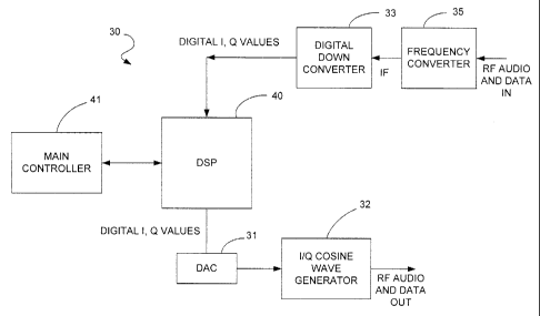
?u FIG. 3 is a block diagram illustrating the components of the transceiver 30
of the
present invention. In accordance with the present invention, a single set of
hardware
components may be utilized for communicating in both the TDMA mode and the
analog
mode over a wireless system, such as the wireless system 1 depicted in FIG. 1.
As can be
seen by comparing the known transceiver 10 of FIG. 2 with the transceiver 30
of the
?5 present invention shown in FIG. 3, several of the hardware components shown
in FIG. 2
have been eliminated. In accordance with the present invention, I, Q pairs are
utilized for
representing data and audio signals in the analog mode. Therefore, the same
hardware
that is utilized for processing and modulating/demodulating audio and data
signals in the
CA 02331912 2001-O1-23
E D Leonard 3-1-22 -8-
TDMA mode may be utilized for analog mode operations. However, it should be
noted
that it is not a requirement of the present invention that the same hardware
be utilized for
analog and TDMA mode operations.
In accordance with the preferred embodiment, generation of the I, Q pairs and
FM
modulation is performed in firmware being executed being executed on a
processor, such
as, for example, a digital signal processor (DSP). The FM modulation and
demodulation
hardware components shown in FIG. 2 are no longer necessary because the
components
that are utilized for TDMA mode operations can also be utilized for analog
mode
operations. The manner in which the transceiver 30 of the present invention
performs
m transmit and receive functions in the analog mode will now be discussed in
detail. Also,
although the present invention is being discussed with reference to performing
analog
mode operations in a TDMA system, it should also be noted that the principles
and
concepts of the present invention can also be applied to perform analog mode
operations
in other types of wireless systems.
~ 5 In order to transmit audio signals in the analog mode, the DSP 40 delivers
digital I,
Q pairs to the DAC 31, which converts the digital I and Q values into analog I
and Q
values. The analog I and Q values are then delivered to an I/Q cosine wave
generator 32,
which converts the analog signals into an in-phase (I) cosine wave and an out-
of phase
cosine wave. The quadrature phase cosine wave is 90° out of phase from
the in-phase
cosine wave. The in-phase cosine wave has an amplitude that is proportional to
the
analog I value and the out-of phase cosine wave has an amplitude that is
proportional to
the analog Q value. The I/Q cosine wave generator 32 sums these cosine waves
for
transmission over air.
When the transceiver 30 is operating in the analog mode and receives an audio
2~ signal, the frequency converter 36 converts the received RF signal down to
an
intermediate frequency (IF). Typically, the RF frequency is in a range of 800
to 900
megahertz (MHz). In this case, the intermediate frequency will typically be
approximately
CA 02331912 2001-O1-23
E D Leonard 3-I-22 -9-
80 MHz. However, the transceiver 30 of the present invention is not limited
with respect
to the RF or IF frequencies, as will be understood by those skilled in the
art.
The digital down converter 33 converts the IF signal into digital I, Q pairs,
which
are then delivered to the DSP 40. The DSP 40 then processes the digital
signals in
accordance with various routines, which are described below in detail.
Generally, the DSP
40 decodes the I, Q pairs and extracts the audio information. The DSP 40
communicates
the extracted audio information to other components of the cell site that
ultimately send
the information to the MTSO.
The tasks performed by the DAC 3 I, the cosine wave generator 32, the digital
m down conversion component 33 when transmitting and receiving data in the
analog mode
are identical to those described above with respect to the transmission and
reception of
audio signals in the analog mode. However, the DSP 40 performs different
functions
depending upon whether the tasks it is performing are associated with audio or
data
signals. When audio signals are delivered to the DSP 40 for transmission over
the wireless
t ~ system, the DSP 40 processes the audio signals accordingly. When the base
station sends
data to the DSP 40, these signals are identified as corresponding to data and
the DSP 40
processes the data signals accordingly.
In accordance with the present invention, the DSP 40 implements a transmit-
audio
routine, a transmit-data routine, a receive-audio routine and a receive-data
routine. By
zo performing these routines in the DSP 40, the need for hardware components
for
performing these different functions is eliminated. The transmit-audio routine
performs
the tasks associated with transmitting audio signals. The transmit-data
routine performs
the tasks associated with transmitting data signals. The receive-audio routine
performs the
tasks associated with receiving audio signals. The receive-data routine
performs the tasks
2~ associated with receiving data signals. Therefore, the DSP 40 is programmed
to execute
software routines that perform these tasks.
A receive-audio routine that is suitable for use with the present invention is
disclosed in U.S. Patent Number 5,694,079, entitled "DIGITAL FM MODULATOR
CA 02331912 2004-06-03
-10-
USING A LAGRANGIAN INTERPOLATION FUNCTION", which is assigned to
assignee of the present application. Therefore, in the interest of brevity, a
detailed
discussion of the manner in which the tasks associated with demodulating and
processing
I, Q pairs representing audio information will not be provided herein.
In FM modulation, the FM modulated signal changes phase in a manner that is
proportional to the amplitude of the input signal. When I, Q pairs are
utilized to generate
an FM modulated signal, the phase of the I, Q pairs must be altered to
generate the
appropriate phase changes in the FM modulated signal. By changing the I and Q
values of
m the I, Q pairs, the phase of the FM modulated signal is changed in a manner
that is
proportional to the amplitude of the input signal. With respect to audio
signals, the
instantaneous frequency of the FM signal is proportional to the current
amplitude of the
audio input. In the digital realm, this is equivalent to causing the phase
change of the next
FM output, which is represented by the next I, Q pair, to be proportional to
the next audio
> > input level. The manner in which the phase change that is needed to
represent the
amplitude of an audio input sample is obtained is well known. Therefore, in
the interest of
brevity, a discussion of the manner in which the phase change representing an
audio input
sample is determined will not be provided herein.
In accordance with the present invention, the I, Q pairs are generated in the
2u following manner. A sample of the audio signal that is being modulated may
be
represented by a(n). A variable, n, corresponds to a sample index. In one
implementation,
which is mentioned merely as an example, n is incremented at a rate of 160
kilohertz
(kHz), which means that 160,000 I, Q pairs are generated by the DSP 40 per
second.
Equation I defines the desired relationship between a(n) and the phase p(n) of
the current
?s sample, n:
p(n) = p(n-1) + k*a(n),
(Equation 1 )
where p(n-1) is the phase associated with the last audio sample, n-l, and k is
an arbitrary
scaling constant that is selected to obtain the desired relationship between
a(n) and the
CA 02331912 2001-O1-23
E D Leonard 3-1-22 -11-
peak frequency deviation of the modulated signal. By re-writing Equation 1 as
follows:
p(n) - p(n-1) = k*a(n), it can be seen that the change in phase is
proportional to the
amplitude of the current audio sample. The I and Q values, I(n) and Q(n),
respectively,
which are values on the unit circle 50 shown in FIG. 4, are obtained from
Equation 2 as
follows:
I(n) = cos(p(n)), and
Q(n) = cos(p(n)-90 degrees). (Equation 2)
The amplitude of the audio signal a(n) is utilized in accordance with
Equations 1 and 2 by
the transmit-audio routine executed by the DSP 40 to determine the I and Q
values I(n)
m and Q(n). The algorithm represented by Equations 1 and 2 can be performed in
a variety
of ways, as will be understood by those skilled in the art. For example, the
algorithm can 4
be executed on the fly as the calculations need to be performed.
Alternatively, a lookup
table can be used to store the I and Q values to enable the appropriate I and
Q values to be
accessed by an index associated with the amplitude of the audio input sample.
The horizontal axis in FIG. 4 corresponds to the I value and the vertical axis
corresponds to the Q value. Each I, Q pair, I(n), Q(n), corresponds to a point
on the unit
circle 50 shown in FIG. 4. The quadrant on the unit circle 50 that the point
is in depends
on the I and Q values. Once the I, Q pairs associated with a frame of audio
signals have
been obtained using the algorithm represented by Equations 1 and 2, they are
delivered to
?o the DAC 31, which converts them into analog values. These analog values are
then
delivered to the cosine wave generator 32. The I/Q cosine wave generator 32
generates
an in-phase cosine wave having an amplitude proportional to the I value and an
out-of
phase cosine wave having an amplitude proportional to the Q value. The out-of
phase
cosine wave is substantially 90° out of phase from the in-phase cosine
wave. These cosine
waves are summed by the I/Q cosine wave generator 32 for transmission over
air.
In accordance with the preferred embodiment, the I and Q values on the unit
circle
50, which will hereinafter referred to as I unit circle and Q unit circle,
respectively, are
not sent directly to the DAC 31. Rather, they are first processed by a
compensation
CA 02331912 2001-O1-23
E D Leonard 3-1-22 -12-
routine to obtain the actual I and Q values that need to be output to the DAC
31 to ensure
that the DAC 31 produces the correct voltage values and to ensure that the
cosine wave
generator 32 produces the correct quadrature waves. The compensation routine
executed
by the DSP 40 converts the unit circle (I,Q) pairs into (I,Q) pairs that cause
the DAC 31
to produce the correct results. The DAC 31 and the cosine wave generator 32
suffer from
the following canonical degradations which are corrected by the compensation
routine:
( 1 ) Different nonzero values for I and Q are typically needed to make the
resulting
voltages output from the DAC 21 equal zero. These nonzero I and Q values are
referred
to herein as loff and Qoff, respectively.
m (2) Different changes in the I and Q values are typically needed to obtain
the same
change in the resulting voltages output from the DAC 31. Hence, the I and Q
values are
scaled differently to compensate for this factor. These scaling factors are
referred to
herein as lamp and Qamp, respectively.
(3) The resulting I and Q signals output from the I and Q generator of the
cosine
i s wave generator 32 are not exactly 90° apart. This phase error is
defined as phase(Q) -
phase(I) - 90. Ideally, this phase error is 0, which will be the case if
phase(Q) is separated
from phase(I) by exactly 90°.
The compensation parameters used to compensate for these degradations
preferably are specified by the main controller 41 through a compensation
message that it
zo sends to the DSP 40. When this message arrives at the DSP 40, the
compensation
routine is called to store these parameters in memory (not shown) in the DSP
40. The
compensation Formulae are derived in the following manner. Ignoring offset
errors, the
following I and Q values (lout and Qout) will be output from the DAC 31 when
the DSP
40 generates Igen and Qgen, which correspond to the I and Q values that must
be
25 generated by the DSP 40 and output to the DAC 31 to ensure that the DAC 31
produces
the correct voltages.
The relationship between Igen, Qgen, lamp, Qamp and the phase error
(phase error), can be seen in FIG. 5. This relationship is expressed by
Equations 3 and 4
CA 02331912 2001-O1-23
E D Leonard 3-1-22 -13-
lout = Igen _ Qgen * sin( phase error)
lamp Oamp
(Equation 3)
Oout = Qgen * cos(phase error)
Qamp -
Igen and Qgen can be expressed as:
I en - Ides + des * sin( phase _ error )
g ( Q cos(phase_error)) lamp, and (Equation4)
Qdes * Qamp
Ogen =
co s( phase _ error )
a The terms Ides and Qdes are the I and Q values that are desired, i.e., the I
and Q values
that should be output from the DAC 31. These values Ides and Qdes are then set
equal to
Ides=I on unit circle and Qdes=Q on unit circle. Igen and Qgen may then be
expressed
as follows, while also correcting for offset errors:
Igen = (I _ unit _ circle * lamp) + (Q -unit _ circle * lamp * sin( phase
error) ) + loff
cos(phase _ error) '
and
Q _ unit _ circle * Qamp
Qgen = cos(phase-error) +Qoff. (Equation 5)
The compensation parameters that a.re provided to the DSP 40 by the main
controller 41
via the compensation message are:
tx i amp = lamp,
t 5 tx_qsec = Qamp l cos(phase error),
tx itan = lamp * sin(phase error) / cos(phase error),
loff , and Qoff
Substituting these parameters into Equation 5, Igen and Qgen can be expressed
as:
Igen = (I- unit circle * tx i amp) + (Q unit circle * tx itan) + Ioff, and
Zo Qgen = (Q unit circle * tx_qsec) + Qoff. (Equation 6)
Therefore, the values for Igen and Qgen, which are the I and Q values that
need to be sent
from the DSP 40 to the DAC 31, can be obtained from Equation 6.
CA 02331912 2001-O1-23
E D Leonard 3-1-22 -14-
One of the advantages of utilizing the compensation routine to obtain
compensated
values for I and Q is that relatively inexpensive hardware, which is more
likely to cause the
aforementioned degradations, can be utilized for the DAC 3 l and the cosine
generator
hardware 32. However, it should be noted that it is not necessary that the
compensation
a routine be utilized. Hardware components that do not cause these
degradations can be
utilized as opposed to utilizing the compensation routine of the present
invention.
Some or all of the compensation parameters may be determined in the factory
prior
to the transceiver being implemented in the field. In order to take into
account
environmental conditions, some of the parameters may be determined in the
field. Each
~ o transceiver typically will require that different compensation parameters
be utilized.
Therefore, some testing will need to be performed to determine the values of
the
compensation parameters that will be.needed to cause the correct FM modulated
signal to'
be output by the cosine wave generator 32. The testing can be accomplished
using tools
such as, for example, a spectrum analyzer. Those skilled in the art will
understand the
manner in which such testing can be performed to obtain the appropriate values
for the
compensation parameters.
The transmit-data routine will now be described with reference to FIG. 6. In
order
to enable the base station to send various types of messages to the mobile
unit, such as
messages indicating power level changes and hand-of~s, the transmit-data
routine of the
?o present invention performs frequency shift keying by generating I, Q pairs
to produce
sequences of 1 s and Os. As stated above, by generating the appropriate
sequence of I, Q
pairs, the phase of the FM modulated signal can be altered. In FSK, 1 s and Os
are
represented by certain phase transitions in the FM modulated signal.
Therefore, by using
Equations l and 2 above, the I, Q pairs needed to generate the appropriate
sequence of 1 s
and Os can be obtained. It should also be noted that, although the transmit-
data routine is
being described with reference to messages being sent from the base station to
the mobile
unit, the transmit-data routine may also be utilized in mobile units for
sending messages
CA 02331912 2001-O1-23
E D Leonard 3-1-22 -15-
from the mobile units to the base stations. This is also true for the transmit
audio, receive
audio and receive-data routines discussed herein.
Four different bit transitions can occur when performing FSK, namely, a 0-to-0
transition, a 0-to-1 transition, a 1-to-0 transition and a 1-to-1 transition.
In accordance
s with the preferred embodiment of the present invention, four lookup tables
are used for
storing I and Q values for the respective transitions. To transition from a
first bit that is a
binary 0 to a second bit that is a binary 0, the first I, Q pair representing
the second bit
must have a phase of 0°. To transition from a first bit that is a
binary 0 to a second bit that
is a binary l, the first I, Q pair representing the second bit must also have
a phase of 0°.
m To transition from a first bit that is a binary 1 to a second bit that is a
binary 0, the phase ,
offset of the first I, Q pair representing the second bit must equal the phase
of the last I, Q
pair representing the first bit. To transition from a first bit that is a
binary 1 to a second bit
that is a binary 1, the phase offset of the first I, Q pair representing the
second bit must
equal the phase of the last I, Q pair representing the first bit.
t 5 Therefore, the phase of the first I, Q pair of a current bit depends on
the phase of
the last I, Q pair of the previous bit. Consequently, by selecting appropriate
I, Q pairs for
the current bit, the desired bit values can be generated. For example, if the
previous bit is
a 0, a 0-to-1 transition can be produced by selecting a first I, Q pair that
produces a phase
of 0° for the next bit. The addresses that are used to index each
lookup table are based on
?u which of these four transitions is occurring and the number of I, Q pairs
that have already
been output to produce the transition (i.e., where the routine is in the
transition).
When the transceiver 30 of the present invention transitions from transmitting
audio to transmitting data, and vice versa, abrupt changes in phase must be
avoided.
Therefore, steps must be taken to ensure that these transitions do not involve
large, abrupt
25 phase changes. In accordance with the present invention, when transitioning
from audio
to data, the transmit-data routine ensures that the phase offset of all of the
I, Q pairs
representing the stream of data is equal to the phase of the I, Q pair
representing the last
audio sample. During the transmit-audio routine discussed above, the DSP 40
stores an
CA 02331912 2001-O1-23
E D Leonard 3-1-22 -16-
indicator of the phase of the I, Q pair representing the current audio sample,
as indicated
by block 6I . The transmit-data routine uses this stored indicator to
determine what the
phase of the first data sample should be, as indicated by block 63. The
transmit-data
routine ensures that the I, Q pair associated with the first sample of data
has the same
phase as the I, Q pair associated with the last sample of audio.
In accordance with the preferred embodiment, the transmit-data routine outputs
I,
Q pairs representing either a 0-to-0 or a 0-to-1 transition for the first data
bit following the
last audio bit. Thus, for the first data bit, the routine assumes that it is
transitioning from a
0. The first I, Q pair in both of these lookup tables has a phase of
0°. From then on, the
o transmit-data routine selects the I, Q pairs from the lookup tables that
provide the
appropriate phase change. A complex multiplication is performed on all of the
I, Q pairs
representing the data samples to cause the phase of the I, Q pairs to be
offset by the phase
of the I, Q pair representing the last audio sample, as indicated by block 65.
Those skilled
in the art will understand the manner in which complex multiplication can be
performed to
i 5 change the phase associated with an I, Q pair to a desired phase.
Ensuring that the first I, Q pair associated with the first data sample has a
phase of
0° facilitates the complex multiplication operations in that the
routine is only required to
ascertain the phase of the I, Q pair representing the last audio sample. In
other words, by
always beginning with a phase of 0° for the first I, Q pair associated
with the first data bit,
2o the routine must simply offset the phase of each I, Q pair associated with
the data bits by
whatever the phase is of the last audio sample. Otherwise, the routine would
have to
determine the phase of the last audio sample and the phase of the first I, Q
pair used from
the table in order to perform the complex multiplication process to offset the
phase of the
data bits. Therefore, forcing the phase of the I, Q pair associated with the
first data bit to
?5 be 0° simplifies the phase offsetting process. However, it should be
noted that this is
simply an elegant, and therefore preferred, way of performing the phase
offsetting process.
Those skilled in the art will understand that the present invention is not
limited to this
preferred embodiment for performing the phase offsetting process.
CA 02331912 2001-O1-23
E D Leonard 3-1-22 -17-
When transitioning from transmitting data to transmitting audio, the transmit-
audio
routine ensures that the I, Q pair representing the first audio sample
following the data has
a phase offset equal to the phase of the last audio I, Q pair that was output
before the
data. This is accomplished by performing a complex multiplication on the I, Q
pair
representing the first audio sample following the data. However, in contrast
to the
complex multiplication operation performed when transitioning from audio to
data, only
the I, Q pair associated with the first audio sample following the data stream
needs to be
multiplied. The phase change performed on the first audio sample will be
implicitly carried
forward on the I, Q pairs representing the subsequent audio samples.
m In accordance with the present invention, it has been determined that the
phase of
the first I, Q pair representing audio following the data only needs to be
offset if the last
bit of data was a 1. If the last bit of data was a 0, a phase offset does not
need to be
performed. The transmit-audio routine simply begins with an I, Q pair having
the same
phase as the phase of the last I, Q pair representing the last audio sample
before the data.
~ 5 As stated above, the phase of the current audio sample is stored by the
transmit-audio
routine. The transmit-audio routine simply uses this phase to determine what
the phase
offset of the first I, Q pair representing the first audio sample following
the data should be.
The transmit-audio routine determines whether the last data bit was a 0 or a I
, as indicated
by block 67. If it was a 0, the transmit audio routine is performed without
performing the
?n phase offset, as indicated by block 69.
It was also determined that, when a phase offset does need to be performed
(i.e.,
when the last data bit was a 1 ), the phase offset is always the same. As
stated above, this
phase offset must cause the starting phase for the transmit-audio routine
following the
data to be equal to the phase of the last I, Q pair representing the last data
sample before
?a the data. This phase offset preferably is predetermined and stored in the
DSP 40 (i.e., it is
hard coded) for use by the transmit-audio routine. Therefore, the transmit-
audio routine
simply utilizes this pre-stored phase offset to perform the complex
multiplication when the
last bit of data is a 1. If the transmit-audio routine determines that the
last data bit was a 1
CA 02331912 2001-O1-23
E D Leonard 3-1-22 -18-
(block 67), then the routine performs complex multiplication on the first I, Q
pair
associated with the first audio sample, as indicated by block 71, using the
pre-stored phase
offset.
The receive-data routine, in accordance with the preferred embodiment, will
now
be described with reference to FIGS. 7 and 8. When a data signal is received
by the digital
down converter 33 shown in FIG. 3, the data is in a format represented by, or
similar to,
the diagram shown in FIG. 7 (as modified by fading and noise). The data signal
is
physically represented as a sequence of (I, Q) values. A data message begins
with an
initial 64-bit dotting sequence 81, which is followed by radio link words
(RLWs) 82. Each
to RLW 82 includes a 37-bit Dotting sequence 83 followed by an 11-bit Barker
sequence 84i
which is followed by 48 bits of data and BCH 85. The BCH bits represent a
check sum.
Each RLW 82 is repeated five times. Therefore, the DSP 40 has five
opportunities to
decode each RLW 82. The Dotting sequence 83 is used for clock recovery and the
Barker sequence is used to determine where the first bit of data 85 begins.
t > As described in the aforementioned Air Interface Standard, the data is
received
from the mobiles in a frequency-modulated (FM) format, and not in the form of
(I, Q)
values as output by box 33 of FIG. 3. Thus, in an initial step, the data is
converted from
the (I, Q) format to FM.
The basic form of the I and Q values is described in Equation (2), above. In a
?u naive approach, it is possible to perform a direct inversion to obtain the
voltage
V(n) _ ~t p(n) by taking, for example, ~t arctan ~ tt ~ However, numerical
noise can
be reduced and computational efficiency enhanced by the following alternate
procedure.
First obtain DI(n) = I(n)- I(n-1), ~Q(n) = Q(n)- Q(n-1), and a signal-strength
estimate
y(n) = I ' (n) + QZ (n) . Then obtain the voltage from V(n) = c I(n)OQ(n) -
Q(n)DI(n)
y(n)
?a wherein c is a scaling constant. In the noisy environment typical of
cellular systems,
individual samples of V(n) are quite unreliable.
CA 02331912 2001-O1-23
E D Leonard 3-1-22 -19-
The several samples of V(n) taken during each bit cell are combined by a
variant of
the procedure described in U.S. Patent No. 4,596,024, commonly assigned
herewith and
hereby incorporated herein by reference. Reference is made to box 27 of FIG. 3
of the
cited patent 4,596,024. The box 27 contains a table of values for a likelihood
ratio DL(t,
s v). According to a currently preferred procedure, DL(t, v) is factored by a
singular value
decomposition (SVD) as described, e.g., in J.J. Dongarra et al., UNPACK Users'
Guide,
SIAM, Philadelphia ( 1979). That is, DL(t, v) ~ U(t) . Z(v), wherein U(t) is a
weighting for
the different samples within a bit cell, and Z(v) is a nonlinear weighting of
the voltage
estimates. The summation B = ~ U(t) ~ Z(V(t)) gives an initial estimate of the
bit. As
~c~ described in the above-cited work by Dongarra, details of U and Z dif~'er
slightly when
detecting Dotting (when the clock is still to be determined) and when decoding
bits.
In the latter case, an additional weighting is used. Because (see FIG. 7
herein)
each word is repeated, the values of B obtained on the different repeats are
again
weighted. This may be represented by the expression ~ WA (B~ ) ~ WB (y~ ) ,
wherein W,a
repeats
weights B; by its distance from nominal, and WB weights by the average signal
strength
during the bit on repeat j.
The Dotting sequences 81, 83 are sequences of is and Os that produce a 5 kHz
waveform, as required by the aforementioned Air Interface Standard. For the
particular
format shown in FIG. 7, the DSP 40 utilizes the initial Dotting sequence 81 to
determine
?o that a data message is being received, and thereafter utilizes the Dotting
sequence 83 of
each RLW 82 to help detect each RLW 83. The DSP 40 detects the Dotting
sequences
81, 83 by measuring the level of 5 kHz energy received and the purity of the
signal. The
level of 5 kHz energy is measured by performing a frequency domain analysis,
preferably
by taking the Fourier Transform of the received signal. The purity of the
signal relates to
2s how much of the signal contains frequencies other than the frequency of 5
kHz. The
purity condition is evaluated by obtaining the signal-to-noise and distortion
(SINAD)
ratio. If the level of 5 kHz energy exceeds a certain threshold level and the
SINAD ration
CA 02331912 2001-O1-23
E D Leonard 3-1-22 -20-
exceeds a certain threshold, the DSP 40 determines that the Dotting sequence
has been
detected and that a data message is being received. These steps are
represented by block
92 in the flow chart shown in FIG. 8.
Once the Dotting sequence has been detected, the DSP 40 determines the phase
of
the 5 kHz signal, which synchronizes the DSP 40 to the start of each data bit.
This is
essentially clock recovery, which enables the DSP 40 to align with the bit
cells. Those
skilled in the art will understand the manner in which clock recovery can be
performed
using the Dotting sequence. In a currently preferred embodiment, this is done
using the
phase of the Fourier transform, which was mentioned above in regard to
detecting
o Dotting. This step is represented by block 94 in FIG. 8. The DSP 40 then
begins looking
for the Barker sequence. Once the DSP 40 has detected the Dotting sequence and
has
performed clock recovery, the DSP 40~has determined that it has located the
Dotting
sequence, but it has not yet determined where it is in the Dotting sequence.
The DSP 40
detects and uses the Barker sequence to determine where the data 85 begins.
The step of
detecting the Barker sequence is represented by block 96 in FIG. 7. The Barker
sequence
84 is a specific sequence of 1 s and Os. The DSP 40 looks for this specific
sequence and,
when it has been detected, determines that the next bit is the first bit of
data 85.
Therefore, the DSP 40 utilizes the Barker sequence to align itself with the
data 85, i.e., to
determine where the first bit of the data 85 begins. This step is represented
by block 98 in
zo FIG. 8.
Once the data 85 has been located, the DSP 40 decodes the data. In order to
decode the data, the processor evaluates the bits of a particular number of
repeats of an
RLW before determining whether any bit represents a binary 1 or a binary 0.
For each
repeat, the processor evaluates each bit to determine whether it is likely to
be a binary 1 or
2 ~ a binary 0. Once the bits have been evaluated for a particular number of
repeats, the
processor uses the results of all of the evaluations to determine whether each
bit is a
binary 1 or a binary 0. In accordance with the preferred embodiment, the DSP
40 looks at
CA 02331912 2001-O1-23
E D Leonard 3-1-22 -21-
each bit of the data 85 for each RLW 82 of the five repeats and generates and
stores a
confidence factor associated with each bit. This step is represented by block
100.
The confidence factor is based on how closely the waveform represents a 1 or a
0
as well as the signal strength associated with the signal. If the waveform is
relatively
noisy, or if the RF signal strength is low, the DSP 40 assigns less weight to
its
determination as to whether the waveform represents a 1 or a 0. If the
waveform has
relatively little noise and if the RF signal strength is relatively high, the
DSP 40 assigns
more weight to its determination as to whether the waveform represents a 1 or
a 0. Once
this process has been performed for each repeat of the current RLW 82, the DSP
40 takes
~ o the sum of the confidence factors associated with each bit for each RLW 82
for all five
repeats and compares the sum to a threshold level, which preferably is 0. If
the sum is
greater than the threshold level, the DSP 40 determines that the bit is a 1.
If the sum is
less than the threshold level, the DSP 40 determines that the bit is a 0.
This process of assigning confidence factors for each of the bits of each of
the five
~ s repeats is also performed for the Dotting and the Barker sequences. For
each of the five
repeats, the DSP 40 obtains a confidence factor associated with each bit of
the combined
Dotting and Barker sequences in the aforementioned manner. Therefore, by the
end of the
five repeats, the DSP 40 has determined whether each bit of the combined
sequence is a 1
or a 0. The steps associated with utilizing the confidence factors to
determine whether the
?u bits are 1 s or Os are represented by block 101 in FIG. 8. As stated above,
the Dotting and
Barker sequences are specific, known sequences. The DSP 40 compares the
results of the
determination to what the combined sequence is known to be and determines the
number
of bit errors that have occurred. This step is represented by block 103 in
FIG. 8. If the
number of bit errors exceeds a predetermined threshold, the DSP 40 aborts
message
25 processing. This step is represented by block 104 of FIG. 8. The DSP 40
could instead
use only the Barker sequence for this purpose, but using both the Barker and
Dotting
sequences provides better results.
CA 02331912 2001-O1-23
E D Leonard 3-1-22 -22-
Although the base station and the mobile unit are both using a 10 kHz clock
frequency, the clocks are not ideal and therefore tend to drift. This could
potentially cause
the DSP 40 to lose its alignment with the data. Therefore, the receive-data
routine
performs a clock tracking routine that enables the DSP 40 to periodically
realign with the
s beginning of the bit cells. In accordance with the preferred embodiment, the
phase is
adjusted every 5 ms. There are 12 samples per bit cell. There are 10 bit cells
per ms.
Therefore, there are 120 samples per ms, which corresponds to 600 samples
every 5 ms.
The inner product is taken for each 120 samples corresponding to each of the
10
respective bit cells per ms. This is done for all 600 samples associated with
the S ms
1 o period. The result of each dot product is used to update an "aggregate
phase shift"
variable. At the end of each 5 ms period, the phase is adjusted in accordance
with the
value of the "aggregate phase shift" variable. Therefore, every 5 ms, the
receive-data
routine realigns the DSP 40 with the beginning of the bit cell.
The present invention also provides a signaling tone detection routine that is
used
to distinguish between when data 85 is being received and when signaling tone
is being
received. Signaling tones of various duration are transmitted from the mobile
unit to the
base station to communicate various types of information to the base station.
Therefore,
when a determination is made that signaling tone has been detected, the DSP 40
will stop
decoding data and prepare to receive a message from the mobile station.
2o Signaling tone is represented by a sequence of all Os or by a sequence of
all 1 s,
which corresponds to a 10 kHz sine wave. When a predetermined threshold level
of 10
kHz energy has been detected for a predetermined period of time, the signaling
tone
detection routine determines that signaling tone has been detected. If the
sequence of data
bits 85 contained in an RLW is ether a long sequence of Os or a long sequence
of 1 s, the
2a sequence could have sufficient 10 kHz energy to cause the processor to
determine that the
sequence represents signaling tone. In order to avoid this problem, the number
of bit
errors in the Dotting and Barker sequences are checked after each RLW to
determine
whether or not data is being received.
CA 02331912 2001-O1-23
E D Leonard 3-1-22 -23-
Generally, if a relatively small number of bit errors are found in the
DottingBarker
sequence, then the signaling tone detector state will be modified to reflect
the fact that no
signaling tone energy has arrived during the receipt of the last RLW.
Conversely, if too
many bit errors are found in the Dotting/Barker sequence, then the signaling
tone detector
state will be modified to reflect any signaling tone energy that has arrived
during the
receipt of the last RLW. The manner in which the signaling tone detection
routine
performs these tasks will now be described with reference to FIG. 9.
The signaling tone detection routine is constantly running and is independent
of the
receive-data routine previously discussed. However, certain state variables
and
U determinations that are made by the receive-data routine are utilized by the
signaling tone ,
detection routine. The signaling tone detection routine uses the determination
made by '
the receive-data routine as to whether or not a data message is being
processed, as
indicated by block 110. As stated above, the receive-data routine knows what
these
sequences should be and makes a determination for each RLW as to whether these
sequences have been detected. Block 110 in FIG. 9 corresponds to this
determination
being made for the first RLW.
Once that determination has been made, a determination is made as to whether
or
not the level of 10 kHz energy has just risen above a predetermined threshold
level for a
predetermined period of time. The level of 10 kHz energy is determined by
performing a
?o Fourier Transform and by comparing the result to the predetermined
threshold level. This
level of energy is stored in the energy level variable. Next, the signaling
tone detection
routine determines whether the energy level has just exceeded the
predetermined threshold
level for a predetermined period of time, as indicated in block 113. If so, an
indicator will
be stored, as indicated by block 114. If, however, the energy level has
already been
z > determined to be above a predetermined threshold level for a predetermined
period of
time, the indicator that signaling tone has just been detected will not be
modified.
A determination is then made at block 115 as to whether a period of 50 ms has
passed, which corresponds to the amount of time required for five repeats of
the RLW
CA 02331912 2001-O1-23
E D Leonard 3-1-22 -24-
If 50 ms have passed, a determination will be made at block 116 as to whether
the initial
Dotting and Barker sequences associated with the latest RLW have been
detected. As
stated above, the receive-data routine determines the number of bit errors
that are in the
Dotting and Barker sequences by using the aforementioned confidence factors
associated
with each bit for all five repeats of the RLW. If the number of bit errors
associated with
the Dotting and Barker sequences is small enough to result in a determination
that those
sequences have been detected, then signaling tone detection routine will
determine at
block 116 that a data message is being received. Any required action will then
be
performed by the DSP 40, as indicated by block 118, and the process will
proceed to the
t a beginning of the routine.
If a determination is made at block 116 that the number of bit errors indicate
that
the Dotting and Barker sequences have not been detected, the process will
proceed to
block 117 and the DSP 40 will use the aforementioned stored indicator in
performing any
required actions associated with the detection of signaling tone. When the
process returns
to block 110, if a determination is made that a data message is no longer
being processed,
the routine will be exited.
It should be noted that the flow charts of FIGS. 8 and 9 are merely function
representations of the manner in which the receive-data routine and the
signaling tone
detection routines are performed. These flow charts are not intended to
represent the
?u actual code that is utilized to implement the functions discussed herein.
However, those
skilled in the art will understand the manner in which the functions
represented by the flow
charts of FIGS. 8 and 9 may be implemented, and that they may be implemented
in a
variety of different ways. Therefore, it will be understood that the present
invention is not
limited to anyparticular computer program for performing these functions.
The manner in which the DSP 40 and the main controller 41 communicate will
now be described. The DSP 40 can be programmed to communicate with the main
controller 41 in such a way that the main controller 41 treats the DSP 40 as
if it were three
independent processors. This enables the DSP 40 to be utilized with a main
controller that
CA 02331912 2001-O1-23
E D Leonard 3-1-22 -25-
has been pre-configured to operate in conjunction with these processors. For
example, if
a main controller has been configured to communicate with a separate encoder
component, a separate decoder component and a separate baseband component, the
DSP
40 can be programmed to spoof the main controller in such a way that the main
controller
operates as if it were communicating with these separate components when, in
fact, it is
only communicating with the DSP 40. The functions associated with the encoder
and
decoder components have previously been described herein. The baseband
component
typically processes the audio signal in both the forward and reverse
directions. The
manner in which a baseband component operates is known in the art of wireless
to communications. Therefore, a detailed discussion of the operations
performed by a
baseband component will not be provided herein.
In accordance with this embodiment, separate queues in the DSP 40 are provided
for each of these separate components. One queue would receive messages from
the main
controller 41 that are intended for the encoder component. Another queue would
receive
~ s messages from the main controller 41 that are intended for the decoder
component.
Another queue would receive messages from the main controller 41 that are
intended for
the baseband component. Each message from the main controller 41 contains a
field that
the DSP 40 utilizes to determine whether the message is an encoder flavor
message, a
decoder flavor message, or a baseband flavor message. The DSP 40 detects these
packets
2o and assigns the messages to the appropriate queue in the DSP 40. The DSP 40
simultaneously and independently processes the decoder, encoder and baseband
messages
on a first-in first-out (FIFO) basis. The bus lines that would have been used
to connect
the main controller 41 to the separate components would instead be connected
to the DSP
40, or to an interface component that is connected to the DSP 40.
2; Of course, it is not necessary that a main controller 41 pre-configured in
this way
be utilized with the transceiver 30 of the present invention. This feature of
the present
invention merely provides flexibility with respect to the manner in which the
present
invention is implemented.
CA 02331912 2001-O1-23
E D Leonard 3-1-22 -26-
It should be noted that the present invention has been described with
reference to
the preferred embodiments, but that the present invention is not limited to
these
embodiments. Those skilled in the art will understand that modifications may
be made to
the embodiments discussed above without deviating from the spirit and scope of
the
invention. For example, the present invention is not limited to any particular
frequencies.
Also, although the DSP 40 has been described as performing all of the decoding
and
encoding tasks, other types of processors may be used for this purpose
provided they have
sufficient processing capability. Also, although the DSP 40 preferably stores
at least some
of the tables and other information that it uses to perform the encoding and
decoding
m tasks, memory that is external to the DSP 40 may be used for this purpose.
Any type of
computer-readable memory device is suitable for this purpose, including solid
state
memory devices, such as read only memory (ROM) and random access memory (RAM),
as well as compact disk read only memory (CD ROM) and magnetic memory devices.
Furthermore, the functions that are performed by the DSP 40 may also be
performed by other types of processing devices or circuits, provided they have
suitable
processing capability. For example, an application specific integrated circuit
(ASIC) may
also be used for this purpose. A circuit comprised solely of discrete hardware
components
could also be configured to perform these tasks. Therefore, the present
invention may be
implemented using any type of hardware or any combination of software and
hardware.
2u All of these possible implementations will be referred to herein generally
as logic. Thus,
the term "logic", as that term is used herein, is intended to denote any type
hardware
implementation and any type of hardware/software implementation that is
capable of being
configured to perform these tasks.
It should also be noted that the present invention is not limited to the
format of the
25 message shown in FIG. 7. Those skilled in the art will understand that the
data message
format can be altered in virtually an infinite number of ways and that the
receive-data
routine can be altered to decode the message accordingly. Those skilled in the
art will
understand that other modifications can be made to the embodiments discussed
above
CA 02331912 2001-O1-23
E D Leonard 3-1-22 -27-
without deviating from the spirit and scope of the present invention. The
modifications
suggested above are merely examples of modifications that can be made.