Note: Descriptions are shown in the official language in which they were submitted.
CA 02331929 2001-01-22
TITLE
Quantum Dot Tunable External Cavity Lasers (QD-TEC Lasers)
FIELD OF THE INVENTION
The present invention relates to the field of photonics, and more particularly
to low-
dimensionality semiconductor laser devices capable of emitting different
frequencies.
BACKGROUND OF THE INVENTION
Presently, very efficient and compact laser sources can be obtained using
semiconductor laser diodes based on 2-dimensional quantum well(s) in their
active gain
region. Such state-of-the-art semiconductor laser diodes can produce hundreds
of
to milliwatts of laser light emitted over a narrow range of wavelengths of a
few nanometers
(nm) or smaller. Typically, to obtain a different wavelength, a distinct laser
diode must be
fabricated with the appropriate quantum well(s) in its active region. For
several
applications, a wide range of wavelengths are necessary. This limits the
usefulness of
semiconductor laser diodes based on quantum wells because the 2-dimensional
density-
of-states of the electronic structure results in a gain spectrum which can be
tuned at most
by tens of nanometers using external cavities, or using integrated tuning
elements.
The current state-of-the-art technology used to obtain laser sources tunable
over
hundreds of nanometers using external cavity configurations with a solid-state
crystal
such as a Ti-Sapphire lasers (Ti-Saph lasers), or with dyes mixed in a liquid
medium (Dye
lasers). These lasers have major limitations because they are not compact and
are very
inefficient since they have to be aligned and optically pumped with another
powerful laser
operated at shorter wavelengths.
There exists a real need for compact and efficient lasers, tunable over a
broad range of
wavelengths for multimedia and telecommunication applications, as well as for
diagnostic
and research/development tools. New applications will also emerge with the
development
and availability of such laser sources.
It is therefore an object of the invention to provide an apparatus and method
capable of
generating laser light tunable over a wide range of wavelengths in a compact
and efficient
way.
CA 02331929 2008-07-31
StJ1vIlVIARY OF THE INVENTION
Unlike the density-of-state of bulk material and of quantum wells, the
electronic
configuration of low-dimensional nano-structures, herein defined as quantum
wires (one-
or quasi-one dimensional structures) or quantum dots (zero or quasi-zero
dimensional
structures), will allow the saturation of their reduced density-of-states over
a wide range
of energies because the total number of available states is orders of
magnitude smaller
than for quantum wells. This will permit the production of population
inversions and
lasing over wide range of wavelengths. Also, it is possible to produce Self-
Assembled
Quantum Dots (QD) by epitaxy using highly strained semiconductors, and to have
good
to control over their zero-dimensional density-of-state. Such quantum dots can
be grown in a
laser diode configuration with conventional techniques, and the carriers will
be injected
electrically in the QD laser diode. To obtain the tunability in such a QD
laser diode
having a wide gain spectrum, an extemal cavity is used. The resulting QD
tunable
external cavity (QD-TEC) laser retains the efficiency and convenience of
conventional
semiconductor laser diodes, and yet is tunable over hundreds of nanometers by
choosing
the low-dimensional electronic structure of the QD and the optical properties
of the
external cavity.
Accordingly in a broad aspect the invention provides laser system comprising a
laser
diode having an active region containing low dimensional quantum structures
for emitting
light over a wide range of wavelengths of at least one hundred nanometers, a
wavelength-
selective element for selecting a wavelength of interest emitted by said laser
diode, and an
external cavity resonant at a wavelength selected by said wavelength-selective
element so
that the system generates laser light at said selected wavelength.
The wavelength-selective element used to tune the laser output may consist of
an a
diffraction grating, a prism, a birefringent element, an etalon, or a
dispersive element.
One dimensional or quasi-one-dimensional structures can be obtained from
coupled
zero- or quasi-zero dimensional structures, or from other techniques which can
produce
quantum wires.
In operation the application of an electric field causes charged-carriers to
be injected
from contact layers into an active region of a semiconductor heterostructure
containing
2
CA 02331929 2001-01-22
quantum dots or quantum wires. Then photons originating from the radiative
recombination of the charged carriers in the active region are emitted. The
photons are
confined in the cavity designed with tunable wavelength-selective elements
which are
adjusted to support a lasing output over the selected wavelengths.
The laser diode and the wavelength-selective element are preferably located
within the
external cavity in such a way that the laser light is emitted from the laser
diode passes
through the wavelength-selective element and resonates within the external
cavity by
passing one or several times through the laser diode and the wavelength-
selective
element, to finally exit out of the external cavity through one or several
outputs. In a
preferred embodiment the laser diode is a quantum dot (QI)) laser diode.
The external cavity may be formed either in part from a facet of the laser
diode, and/or
in part from the said wavelength-selective element as an output-coupler,
and/or from
specially designed optical components as high reflectors, and/or folding
mirrors, and/or
output couplers.
The QD laser diode preferably comprises multiple layers of semiconductor
materials
including a least one quantum dot layer in an active region between an
electron emitter
layer, allowing the injection of electrons towards the quantum dots, and a
hole emitter
layer, allowing the injection of holes towards the quantum dots. The
composition and
doping of the materials is chosen so that the relative optical constants,
bandgaps, and
conductivity of the layers establish an effective guiding of the optical modes
in a cavity
formed perpendicular to the plane of the layers, as well as efficient carrier
injection when
an electric field is applied with the proper forward-bias polarity.
In the case where multiple quantum dot layers are used in the active region,
barriers
separate the quantum dot layers. The electron and hole emitter layers are
preferably doped
n-type and p-type respectively to act as a reservoir of charged carriers and
to conduct the
current necessary for the operation under bias. The electron and/or hole
emitter layers can
be composed of several layers or regions to vary the composition and/or
doping, to
optimize the optical and electrical properties of the QD laser diode.
The active region is preferably not doped to minimize loses of the guided
optical
modes. Intermediate layers with chosen bandgap and doping can also be
introduced
3
CA 02331929 2001-01-22
between the active region and the emitter layers to tailor the optical guiding
and the
optical and electrical properties of the laser diode. The current injection
and the optical
mode guided in the QD laser diode material are preferably confined laterally
to tailor the
electrical, thermal, and optical characteristic of the QD-TEC laser. The
current injection
in the QD laser diode material might preferably be confined longitudinally to
tailor the
electrical, thermal, and optical characteristic of the QD-TEC laser. The
longitudinal
confinement of the optical mode guided in the QD laser diode material is
preferably
adjusted by changing the reflectivity of a front and a back facet individually
to tailor the
electrical, thermal, and optical characteristic of the QD-TEC laser. It might
be preferable
to regulate the temperature and/or remove excess heat generated by the
operation of the
QD laser diode with the help of a temperature regulating device.
The wavelength-selective element is preferably designed to be adjustable to a
bandpass over the gain spectrum of the QD-TEC laser. For the wavelengths
selected in
the bandpass, lasing will be achieved from a net optical gain which will be
obtained
before the photon escape the cavity, whereas the wavelengths outside the
bandpass will
not lase because the attenuation will be larger than the gain. The selected
bandpass can be
changed by simply adjusting the wavelength-selective element to obtain lasing
at the
various wavelengths available from the gain spectrum of the QD-TEC laser. In
some
embodiments, it might be preferable to build the wavelength-selective tuning
element
integrated to the QD laser diode.
The external cavity preferably provides the appropriate optical feedback to
yield
tunable lasing over a large portion of the gain spectrum of the QD laser
diode. It may
comprise at lease one back mirror and one output coupler but might use more
complex
configurations with several folding minrors and/or output couplers to provide
the desired
optical characteristic and mode profiling functions. In some embodiments, it
might be
preferable to integrate part of the external cavity into the QD laser diode
and/or to the
wavelength selective tuning element.
Also, the size/shape of the quantum dots and the number of quantum dots per
unit area
are adjusted from the growth parameters in conjunction with the choice of
quantum dot
material, of barrier materials, of the number of quantum dot layers, of
extexnal cavity
parameters, and of wavelength-selective element to achieve the desired tuning
range and
4
CA 02331929 2008-07-31
wtlile optimizing the lasing efficiency for the wavelengths of interest.
Similarly, the
choice of the barrier material, the doping profiles, potential height, and
barrier thickness is
adjusted in conjunetion with the quantum dot size to set the gain spectrum of
the QD laser
diode, to select a balance the laser efficiency and modulation speed, and to
achieve the
desired growth mode in the self-assetnbling growth. For multiple layers of
quantum dots
very thin barriers result in coupled zero-dimensional states in vertically
self-organized
quantum dots; thicker barriers result in isolated zero-dimensional states in
vertically self-
organized quantum dots, and thick barriers will result in isolated zero-
dimensional states
in uncorrelated independent quantum dot layers.
to In another aspect the invention provides a method of generating tunable
laser light over
broad spectral ranges from a laser diode, comprising using electrical power to
generate laser
emission extending over a wavelength range of at least one hundred nanometers
from a
low-dimensionality laser diode which has been designed with an active region
having
semiconductor quantum entities with low-dimensionality energy levels as
established by
ts the size and composition of the quantum entities and the height of the
confining potential
of the barriers placing the said low-dimensionality laser diode in an external-
cavity with a
wavelength-selective element and tuning said wavelength-selective element to
obtain the
desired output wavelength within the tunable range of the laser.
20 In a preferred fonn of the invention the layers of the semieonductor
materials are
grown on a substrate from materials consisting essentially of gallium, indium,
aluminum,
arsenic, phosphorous, and possibly nitrogen, using known techniques such as
molecular
5
CA 02331929 2001-01-22
beam epitaxy, or metalorganic chemical vapor deposition, or chemical beam
epitaxy, with
dopant such as silicon, beryllium, or others. On GaAs substrates, the quantum
dot
material can be InGaAs, AlInAs, InP, or other alloys of AIGaInAsP, with
barriers of
AlGaAs or AlGaInP. On InP substrate, the quantum dot material can be InGaAs.
Alloys
with nitrogen can be used with the above III-V in cases where different band
gap
materials are desirable. On group IV substrates, Si can be used for the
barrier, with the III-
V alloys mentioned above for the quantum dot material. The substrate is needed
to give
structural integrity to the very thin layers of the QD laser diode and to
allow proper
crystal growth.
The QD-TEC laser is preferably powered by electrical energy, and lasing at
various
wavelengths is obtained by adjusting the tuning element with the help of some
mechanical components or some electro-optical actuating devices which can be
calibrated
and/or computerized. The optical characteristic of the output laser beam are
preferably
adjusted with the parameters of the external cavity. The zero-dimensional
density-of-state
which dictates the gain spectrum of the QD-TEC laser is controlled from the
symmetry
and shape of the self-assembled quantum dots which preferably takes a form
resembling
an hemispherical cap, a lens shape, a disk shape, a pyramidal or truncated
and/or rounded
pyramid shape. The self-assembled quantum dots are preferably obtained with
the
spontaneous island formation during the epitaxy of highly strained
semiconductor
materials. The details of the self-assembling growth are preferably arranged
to establish
the shape, symmetry, and size of the quantum dots and therefore set the
quantum dot
energy levels to optimize the lasing in the desired spectral range.
The low-dimensionality density-of-states can spans a wavelength range as small
as
l Onm or as large as 500nm. The specified range can be set at wavelengths
between
0.4micron to 2.Omicron, by using a GaAs substrate, an InP substrate, or
another
appropriate substrate, and by using A1,M,(,_xõ)Ga(,_xWx,_xõ)Inx,As(,,.)Pxõ
semiconductor alloys
and/or nitrogen containing alloys.
BRIEF DESCRIPTION OF DRAWINGS
The invention will now be described in more detail, by way of example, only
with
reference to the accompanying drawings, in which:-
6
CA 02331929 2001-01-22
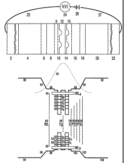
Fig. I is a partial, greatly magnified cross-section view of an example of a
layer
structure for a quantum dot laser diode, with a corresponding schematic of the
energy
level diagram depicting some of the transitions which can be used for the
lasing;
Fig. 2 is a top-view schematic of the principal elements of a QD-TEC laser
giving an
example for one of the possible configurations;
Fig. 3 is an example of spectrum obtained with a quantum dot laser
demonstrating
lasing at lambda - 965nm, in the lower zero-dimensional states, at a
wavelength about
one hundred nanometers away for the shortest achievable wavelength which would
correspond to the wetting layer transitions as shown in Fig. 4. The inset
demonstrates the
io tuning achieved between 880nm and 965nm.
Fig. 4 is an example of spectrum obtained with a quantum dot laser
demonstrating the
complete saturation of all the zero-dimensional states over a wavelength range
of
hundreds of nanometers and with lasing on a wetting layer transition at lambda
- 865 nm.
DETAILED DESCRIPTION OF THE PREFERRED EMBODIMENT
Fig. 1 shows a schematic for the quantum dot laser diode portion of the QD-TEC
laser
in accordance with the invention. Such a diode comprises multiple layers of
semiconductor materials which are depicted in the upper part of fig. 1,
together with the
corresponding energy band diagram shown in the lower part of fig. 1. In the
band
diagram, the vertical direction represents the energy of the carriers in the
structure, and
the horizontal direction represents the position of the carriers within the
laser structure.
The layers are very thin; for instance in a preferred form of the device, the
thickness of a
quantum dot together with the wetting layer which forms below the quantum dots
10, 14
is about 4.5 nanometers or smaller. Hence, it is necessary to provide a
substrate to grow
the layers and to give structural integrity to the device. The substrate can
be electrically
conducting or insulating, and will typically have a thickness between 0.1 and
1 mm. The
substrate will preferably be covered with a buffer layer which also serves to
initiate
proper growth conditions during the epitaxy.
The layers include conducting semiconductor contact layers 2 and 22, on the
outside
of the structure, which serve as sources of charged carriers and are connected
to an
external source of electrical power 26 by using metal contacts (not shown) an
wires 23
7
CA 02331929 2001-01-22
and 27 respectively. Lithography and etching techniques such as wet etchings
or dry
etchings after masks patterning are used to make the metal contacts to the
contact layers.
The contact layers 2 and 22 will preferably be doped to provide carriers and
conductivity,
and can be composed of many layers of varying thickness, composition, and
doping
profiles to optimize the semiconductor morphology and the device performance.
For
example, the substrate used for the epitaxial growth can be used as part of
one of the
contact layer. Also preferably, one side of the structure will be doped n-type
with
electrons whereas the other side will have to be doped with the opposite
polarity, p-type
with holes. In the case for which a doped substrate is used for the epitaxy
and is part of
the contact layer 2 or 22, then that contact layer will preferably be doped of
the same type
as the substrate, whereas the other contact layer will preferably be doped
with the
opposite type.
Next layers towards the inside of the structure are the electron and hole
emitting
layers 4 and 20. As in the case of the contact layers, the electron and hole
emitting layers
i5 4 and 20 will preferably be doped to provide carriers and for conductivity.
The doping of
layers 4 will preferably be of the same type as the one of layer 2, and
similarly the doping
of layers 20 will preferably be of the same type as the one of layer 22. They
can also be
composed of many layers of varying thickness, composition, and doping profiles
to
optimize the semiconductor morphology and the device performance, as well as
to
optimize confinement of the carrier injected electrically in the active region
in the inside
layers. The electron and hole emitting layer will therefore preferably have a
high bandgap
compare to the layers more toward the inside. The major features of the
resulting band
edge profiles are depicted in the energy diagram for layer 4 for the
conduction band 82,
and for the valence band 94. Similarly, the major feature of the band edge
profiles are
depicted for layer 20 for the conduction band 92, and for the valence band
104.
Intermediate layers 6 and 18 with chosen bandgap and doping can also be
introduced
between the active region and the emitter layers to tailor the optical guiding
and the
optical and electrical properties of the laser diode. A possible band edge
configuration is
depicted 84, 90, 96, 102. The composition and doping of the materials will be
chosen so
that the relative optical constants, bandgaps, and conductivity of the layers
will establish
an effective guiding of the optical modes in a cavity formed perpendicular to
the plane of
8
CA 02331929 2001-01-22
the layers, as well as efficient carrier injection when an electric field is
applied with the
proper forward-bias polarity (V) yielding an electrical current I(V) 24.
At the core of the structure, in the active region, is one or more quantum dot
layers 10
and 14 (fig. 1 illustrate the case where two layers are used), separated by
barrier(s) 12,
and confined on each side with barriers (9 and 8), and (15 and 16). The active
region is
preferably not doped to minimize loses of the guided optical modes 28, but low
doping
might be used to optimize some device performances such as modulation speed.
Also
preferably, the size and shape of the quantum dots, and the number of quantum
dots per
unit area are adjusted from the growth parameters in conjunction with the
choice of
quantum dot material (10, 14), of barrier materials (8, 9, 12, 15, 16), of the
number of
quantum dot layers, of external cavity parameters, and of wavelength-selective
element to
achieve the desired tuning range and while optimizing the lasing efficiency
for the
wavelengths of interest. Similarly, the choice of the barrier material (8, 9,
12, 15, 16), the
doping profiles, the potential height for the electron (86, 88) and for the
holes (98, 100),
and the thickness of the barriers (8, 9, 15, and 16) and the spacer layer (12)
are adjusted in
conjunction with the quantum dot size to set the gain spectrum of the QD laser
diode, to
select a balance the laser efficiency and modulation speed, and to achieve the
desired
growth mode in the self-assembling growth. For example, for multiple layers of
quantum
dots, very thin barriers 12 will result in coupled zero-dimensional states in
vertically self-
organized quantum dots, thicker barriers 12 will result in isolated zero-
dimensional states
in vertically self-organized quantum dots, and thick barriers 12 will result
in isolated zero-
dimensional states in uncorrelated independent quantum dot layers.
In particular, the amount of semiconductor material required to form the self-
assembled quantum dots (10, 14, etc.) depends on the relative strain between
the substrate
and the quantum dots. The number of quantum dots per unit area can be adjusted
by
varying the amount of material deposited in the quantum dot layers. The size
of the
quantum dots can be adjusted from the substrate temperature used during the
growth of
each quantum dot layers. For example, in the exemplary embodiment, due to the
small
size of the quantum dots, quantum mechanics will dictate the values of energy
levels (30,
32, 34, 36, 38, 50, 52, 54, 56, 58) localized in the low band gap material
(68) by the
barriers (9, 12, 15). The shape of the zero-dimensional potential gives rise
to a series of
9
CA 02331929 2001-01-22
, & (30, 32, 34, 36, 38
discrete, atomic-like, energy levels for the electrons s,,, p,, d, fe
respectively), and for the holes Sh, Ph, dh, fe, gh (50, 52, 54, 56, 58
respectively), below the
(40) and WLh (60) for the electrons and holes respectively.
wetting layer subband WL,
For self-assembled quantum dots, the degeneracy of these levels is typically
2n where n is
the index of the level with, n= 1 for the ground state S, n= 2 for the first
excited state P,
etc. where the factor of 2 comes from the spin degeneracy, and the factor n
originates
from the various allowed angular momentum. The self-assembled quantum dots
effectively give a zero-dimensional potential with a quasi-parabolic
confinement, and
consequently the energy spacing between the adjacent levels (also called the
intersublevel
spacing) is roughly constant for the various levels.
The number of allowed energy levels and intersublevel spacing is determined by
the
shape and size of the quantum dot, the height of the confining potential
between the
barriers (9, 12, 15) and the quantum dot (10, 14), and by the carrier
effective mass.
Experimental assessment of these energy levels can be obtained independently
by probing
the interband transitions and observing the state filling in photoluminescence
or
electroluminescence. The carriers introduced by the carrier injection fill the
quantum dot
energy levels in accordance with the level degeneracy, a rule similar to the
atomic Hund's
rule for filling orbitals, and Coulomb interaction and renormalization
energies. For
example, first the ground states s, (30) or sb (50) can each accommodate 2
carriers, one
spin up, and one spin down, then the first excited states p, (32) or Ph (52)
can
accommodate 4 carriers 2 spin up and 2 spin down, etc. The total number of
available
states is therefore given by the number of states per QDs for the energy range
of interest,
taking into account the degeneracy of the levels, multiplied by the density of
QD in the
layers which can be varied between 108 to 1010 cm Z. This is typically about 2
orders of
magnitude lower than for 2-dimensional quantum well structures, and therefore
it is
possible to saturate the states over a much wider energy range for the quantum
dot laser
diode.
Radiative recombination of the allowed 0-dimensional and 2-dimensional
transitions
between electrons and holes which occupy these states will yield photon
emission. For
3o example, in a simplified picture, the emission spectrum can preferably be
classified as the
S (70), P (72), D (74), F (76), G (78), and WL (80) transitions, as depicted
in fig. 1. The
CA 02331929 2001-01-22
emission spectrum from a single quantum dot would therefore be principally a
discrete set
of very narrow emission lines. Exciton, multi-exciton, many carriers, and
similar effects
can also slightly perturbed the spectral position of these emission lines.
Also, a quantum
dot laser diode will preferably operate with many quantum dots (typically many
millions)
instead of a single quantum dot, each of which can be slightly different from
the others
because of inhomogeneous broadening during the self-assembled growth. These
effects
and the inhomogenous broadening are preferably adjusted to obtain an emission
and gain
spectrum which can continuously cover a wavelength range hundreds of
nanometers wide
from the S transition 70 to the WL transition 80 (see below fig. 3 and 4). The
reduced
lo zero-dimensional density-of-states of the quantum dots will allow to
saturate the lower
states and to obtain lasing in the upper transition at shorter wavelength as
well as for the
lower states at longer wavelengths by varying the wavelength-selective element
of the
QD-TEC laser.
As mentioned above, in a preferred form of the invention the layers of the
semiconductor materials are grown on a substrate from materials consisting
essentially of
gallium, indium, aluminum, arsenic, phosphorous, and possibly nitrogen, using
known
techniques such as molecular beam epitaxy, or metalorganic chemical vapor
deposition,
or chemical beam epitaxy, with dopant such as silicon, beryllium, or others.
On GaAs
substrates, the quantum dot material can be InGaAs, AlInAs, InP, or other
alloys of
AlGaInAsP, with barriers of AIGaAs or AlGaInP. On InP substrate, the quantum
dot
material can be InGaAs. Alloys with nitrogen can be used with the above III-V
in cases
where different band gap materials are desirable. On group IV substrates, Si
can be used
for the barrier, with some of the III-V mentioned above for the quantum dot
material.
In fabricating the laser diode, a barrier material and an active quantum dot
material are
first selected such that the degree of lattice-mismatch dictates a critical
thickness required
to obtain spontaneous island formation, and the bandgap difference determines
a possible
number of confined states in conjunction with the energy spectrum of the low-
dimensional states.
Next some thickness of the barrier material is grown in the active region
between the
electron emitting layer and the hole emitting layer on a substrate. The
electron and hole
emitting layers are chosen to have a lattice constant close to that of the
substrate.
11
CA 02331929 2001-01-22
The quantum dot material is grown at a specified growth rate at a temperature
which
will produce quantum dots having the appropriate size and shape to obtain said
low-
dimensionality density-of-states. This growth is then stopped after the
desired number of
quantum dot per unit area is reached. Then, one waits a specified amount of
time to allow
for the self-assembling growth to form the quantum dots in shapes and sizes
which will
give the low-dimensionality density-of-states.
Finally some thickness of said barrier material is grown to cover the quantum
dots and
return to a planar growth front at a substrate temperature which may be varied
during the
growth and which will optimize the quality of the quantum dots.
The last steps may be repeated as necessary to build up multiple quantum
layers.
In the exemplary embodiment of the invention, the substrate is GaAs; the
quantum dot
layers (10, 14, etc) consist essentially of Inx,Ga,_x,As wherein xl equals
0.15 to 1,
preferably about 0.5 to 1 and specifically 1; the barriers (8, 16) consists of
A1,,,Ga,_,,,As
with x2 equals to 0 to 1, preferably about 0 to 0.4, and specifically 0.33;
the barriers (9,
12, 15, etc) consists of A1.2Ga,.,2As with x2 equals to 0 to 1, preferably
about 0 to 0.4, and
specifically 0. The electron and hole emitting layers are preferably doped n-
type and p-
type respectively, and made of Al.Ga,_,As with x3 equals to 0.1 to 1,
preferably about
0.3 to 0.8, and specifically 0.7. Intermediate layers 6 an 18 are used in the
exemplary
embodiment using composition profiles gradually going from the composition of
the
electron and hole emitting layers 4, 20 to the one of the barriers 8, 16.
The selected parameters will preferably result in materials having an
effectively
higher index of refraction and lower bandgap in the active region (8, 9, 10,
12, 14, 15, 16)
to confine the carriers and the optical wave together in the gain region. The
size/shape and
composition of the quantum dots, and the thickness and height of the barriers,
is selected
to obtain the desired 0-dimensional density-of-state and gain spectrum for the
QD-TEC
laser. In the exemplary embodiment of the invention, the substrate is doped n-
type and
part of the contact layer 2, the carriers for the electron emitting layers 4
are provided by
silicon doping, the bandgap and the doping is reduced in the intermediate
layer 6 as
shown by 84, 96, the active region is not doped, and a similar scheme is use
for the
intermediate layer 18, the hole emitting layer 20 and the contact layer 22 but
using
beryllium doping to provide the carriers.
12
CA 02331929 2001-01-22
Fig. 2 illustrates an example of how an external cavity and a wavelength-
selective
element can be configured to tune the output wavelength of the QD-TEC laser.
The
quantum dot laser diode 36 is aligned between reflectors 30 and 32, the
wavelength-
selective element 34 discriminate the optical path of the various wavelengths.
Optical
elements 36, 38 can also be used to determine the beam path outside the laser
diode cavity
40, and to initiate the waveguiding inside the laser diode cavity 40. Several
configurations
are possible, but fig. 2 exemplifies one of the possible embodiments using a
diffraction
grating for the wavelength-selective element 34. For such an embodiment, the
optical
element 36, 38 will preferably be lenses used to provide the desired optical
characteristic
and mode profiling functions, and to collimate the photons existing the laser
diode. One
side of the collimated beam 44 is incident on the diffraction grating 34 and
at an angle 0.
The grating then disperses the light mainly in a preferred intensity ratio
between a zero-
order diffraction 46 and a first-order diffraction 48. The wavelength in the
zero-order
diffraction are not dispersed and this beam 46 can be used as the (or one of
the) output
beam of the QD-TEC laser. The wavelengths in the first order beam 48 are
dispersed in
space and a spatial filter 50 can be used to let only the desired wavelengths
resonate in the
cavity. The wavelength tuning can be achieved by turning the grating angle 0
or
preferably by displacing the spatial filter 50, either of which will vary the
wavelength
bandpass which is allow to resonate in the cavity. The adjustment of the
tuning element
can be made with the help of some mechanical components or some electro-
optical
actuating devices which can be calibrated and/or computerized.
The current injection and the optical mode guided inside the QD laser diode
material
are preferably confined laterally 52, 54 to tailor the electrical, thermal,
and optical
characteristic of the QD-TEC laser. This can be achieved with lithography and
etching
techniques such as wet etchings or dry etchings after masks patterning which
are used to
make the metal contacts 56, 58 to the contact layers. The current injection in
the QD laser
diode material might preferably be confined longitudinally 60, 62 to tailor
the electrical,
thermal, and optical characteristic of the QD-TEC laser. The longitudinal
confinement of
the optical mode guided in the QD laser diode material is preferably adjusted
by changing
the reflectivity of a front 62 and a back 64 facet individually to tailor the
electrical,
13
CA 02331929 2001-01-22
thermal, and optical characteristic of the QD-TEC laser. A longitudinal mode
regulator 13
can be adjusted to match a proper cavity mode for the selected wavelengths.
It might also be preferable to regulate the temperature and/or remove excess
heat
generated by the operation of the QD laser diode with the help of a
temperature regulating
device. Also, obviously the various component layers (2, 4, 6, 8, 10, 12, 14,
etc.) are
aligned and fixed in space on a rigid and stable platform which is designed
with the
proper adjustments and mechanisms for moving the parts which are displaced
during the
tuning of the QD-TEC laser.
Also as mentioned above, fig. 2 exemplifies one of the many possible
embodiments,
and for example in some embodiments, it might be preferable to build the
wavelength-
selective tuning element integrated to the QD laser diode by using lithography
techniques
to produce gratings directly on the semiconductor, and which could be tuned
using
electric fields and/or currents in part of the device. Also, in some
embodiments, it might
be preferable to build part of the external cavity integrated to the QD laser
diode and/or to
the wavelength selective tuning element. For example, the reflector 30 and the
optical
element 36 are preferably eliminated by producing a reflector with the
appropriate optical
properties directly on the laser diode facet 64 using a combination of
deposited thin films.
Similarly the optical properties of the facet 62 can be adjusted by depositing
thin films to
optimize the device performance. Also the reflector 32 can be eliminated by
folding the
first order beam 48 directly back on the laser diode beam 66. The preferred
geometry and
the optical properties of the various elements will be dependent of the
desired tuning
range and power, and the desired spatial, temporal, and spectral mode profile
for the QD-
TEC laser. For example, the reflectivity and the transmission spectra of the
reflector 30
and 32, and/or of the facet 60 and 62, as well as the grazing angle of the
grating 34, will
have to be adjusted according to the wavelength range of the QD-TEC laser
Fig. 3 demonstrates the case for a quantum dot laser diode having seven layers
of
InAs quantum dots (10, 14, etc.) with GaAs barriers (9, 12, 15, etc.), with
A1o.35Gao.65As
barriers (8, 16), and with Ala.,Gao.3As electron (4) and hole (20) emitting
layers barriers,
grown on a GaAs substrate which is part of the contact layer 30. For this
example, the
metal contact (58 in fig. 2) is 60 micron wide and 5mm long on top of GaAs
contact layer
(22). Cleaved facets with no facet coatings (60 and 62 in fig. 2) are used
here. The
14
CA 02331929 2001-01-22
resulting 0-dimensional transition (S, P, D, F, and WL) can be observed at the
bottom of
fig. 3 in the electroluminescence (EL) and photoluminescence (PL) spectra
obtained at
different excitation intensity and current. The top of the fig. 3 demonstrates
lasing at
lambda - 965nm, in the lower zero-dimensional states, at a wavelength about
one hundred
nanometers away for the shortest achievable wavelength which would correspond
to the
wetting layer (WL) transitions. The threshold current density to obtain lasing
in this case
is 13.5 A/cm2, resulting in a range of saturated zero-dimensional states, and
a range of
saturable zero-dimensional states as indicated.
A QD-TEC laser based on such a quantum dot laser would benefit from a gain
spectrum about l00nm wide and its output could be tune over that range. For
example,
the inset shows tuning between 880nm and 965 nm obtained by changing the
length of the
laser diode cavity. Fig. 4 shows a similar quantum dot laser where only one
layer of
quantum dot was used, and where the size and shape of the quantum dot was
changed. It
results in a wavelength range of -- 260nm between the S and WL transition. The
complete
saturation of all zero-dimensional states over about 260 nm is demonstrated
with lasing at
871 nm close to the WL transition (curve v of fig. 4). A QD-TEC laser based on
such a
quantum dot laser would benefit from a gain bandwidth about 260 nm wide and
its output
could be tune over that range by using wideband optics and reflectors.
The QD-TEC laser is based on low-dimensional, such as zero-dimensional
heterostructures (i.e. quantum dots) and can benefit from the properties
unique to
quantum dots. One obvious advantage gained from using quantum dots is that the
QD-
TEC laser is tunable over wide ranges of wavelengths. However, one-dimensional
heterostructures, i.e. quantum wires can also be used to advantage. The self-
assembled
growth method used offers a wide range of possible materials with large
lattice
mismatched between the semiconductors, therefore increasing the choice of
available
material for fabrication and thus the available emission spectra. In addition,
the QD-TEC
laser will have good efficiency because it is based on semiconductor laser
diode
technology.
The tunable lasing range of the described laser may be in the visible red
region, or the
near infrared region of the spectrum. For example, the tunable lasing range
may be in the
region of the spectrum close to 1.3micron, in the region of the spectrum close
to 1.4-
CA 02331929 2001-01-22
1.7micron, in parts or the complete spectral region between 0.6 to 2.0
microns, or in parts
or the complete spectral region between 0.3 to 2.5 microns.
The external cavity, and/or the said low dimensionality laser diode, and/or
the said
wavelength-selective element can be adapted to be with high modulation speed
or to be
used mode-locked.
Whereas particular embodiments of the invention have been described for
purposes of
illustration, it will be evident to those skilled in the art that numerous
variations of the
details may be made without departing from the invention.
16