Note: Descriptions are shown in the official language in which they were submitted.
CA 02331954 2004-11-02
1
METHOD AND APPARATUS FOR STABILIZING TRANSIENT CONTROL
IN AMPLIFIED OPTICAL NETWORKS
TECHNICAL FIELD
The invention relates generally to optically amplified lightwave
communication systems and, more particularly, to controlling transient
response in
such systems.
BACKGROUND OF THE INVENTION
To meet the increasing demands for more bandwidth and higher data rates in
today's networks, wavelength division multiplexing (WDM) is being used
extensively
in long haul optical transmission systems and is being contemplated for use in
short
haul applications, such as metropolitan area networks and the like. As is well
known,
WDM combines many optical channels each at a different wavelength for
simultaneous transmission as a composite optical signal in a single optical
fiber.
Optical amplifiers are commonly used in lightwave communication systems as
in-line amplifiers for boosting signal levels to compensate for losses in a
transmission
path, as power amplifiers for increasing transmitter power, and as pre-
amplifiers for
boosting signal levels before receivers. In WDM systems, optical amplifiers
are
particularly useful because of their ability to amplify many optical channels
simultaneously. Rare earth-doped fiber optical amplifiers, e.g., erbium-doped
fiber
amplifiers, are commonly used in WDM systems, although other types of optical
amplifiers, e.g., semiconductor optical amplifiers, can also be used.
In an optically amplified WDM system, signal power transients in a WDM
signal can be a significant problem. Signal power transients may occur as a
result of
adding or dropping individual optical channels, network reconfigurations,
failures or
recovery from failures, and so on. For example, adding or dropping individual
channels of a WDM signal may cause changes in input power to an optical
amplifier,
which in turn results in changes in gain as well as fluctuations of power
levels in
surviving optical channels, i.e., those optical channels that are still
present in the
WDM signal after an add/drop has occurred. Stated otherwise, because optical
CA 02331954 2004-11-02
2
amplifiers in WDM systems are typically operated in saturation, the output
power of
an optical amplifier will not necessarily change in a corresponding manner
with input
power changes and, as a result, optical power in the individual surviving
channels will
fluctuate undesirably. These power fluctuations may result in unnecessary
protection
switches in the network, transmission stabilization problems, unacceptable bit
error
rate degradation if power variations are not within the dynamic range of
receiver
equipment, and other power-related problems.
Several gain control schemes have been proposed for reducing the effects of
power transients. For example, U.S. Patent No. 6,366,393, issued April 2,
2002,
entitled "Fast Gain Control for Optical Amplifiers ", describes one approach
for
reducing the effects of signal power transients in an optically amplified WDM
network. In this approach, per-channel gain of individual optical channels is
kept
relatively constant despite changes in input power at the optical amplifier,
such as
when individual optical channels of the WDM signal are added/dropped. By
maintaining relatively constant per-channel gain in an amplified WDM signal
despite
changes in input power at the optical amplifier, power fluctuations are
substantially
reduced in surviving optical channels of the WDM signal.
However, even when a gain control scheme is employed, there still may be
problems relating to power transients that may perpetuate in the network
depending
on network topology and other factors. For example, gain-controlled optical
amplifiers may compensate for large power transients, but typically will not
achieve
complete suppression of low level signal variations. In particular, so-called
remnants
of the power transients may still perpetuate around the network. As used
herein,
power transient is meant to correspond to the initial power-affecting change
where it
is desirable to respond to the transient event, e.g., the aforementioned gain
control to
respond to a change in channel count. Remnants of power transients, or
CA 02331954 2001-O1-22
DEMCIN 11-2-1-3-1 3
artifacts as they are sometimes referred to, are typically a result of
imperfect
approximations that are made when responding to the initial transient event,
e.g.,
approximations of the amount of required gain adjustment. Remnants may be in
the
form of oscillations of the initial power transient that perpetuate as an
error signal
around the network. Unless attenuated, these remnants may de-stabilize or
otherwise disturb the network. For example, remnants that are continuously
routed
around a network may trigger unwanted effects if, for example, a subsequent
optical
amplifier cannot distinguish the remnants from the initial power transient
caused by
an actual transient event.
1o Remnants can be especially problematic in particular network topologies,
such as a ring network. A WDM ring network, as is well-known, typically
includes
a plurality of interconnected nodes, at which WDM optical signals may be
amplified
and at which individual optical channels may be added or dropped. In a WDM
ring
network, remnants may continue to circulate aa~ound the ring getting further
amplified as they pass through subsequent nodes. nonsequently, the probability
of
remnants triggering an undesirable response increasca in a network topology
such as
a ring. Moreover, during amplification, well-knovrn cross-saturation effects
(e.g.,
gain at a wavelength is affected by power present at other wavelengths) may
imprint
the relatively low frequency components of ampliW de variations of a signal at
one
2o wavelength on signals at other wavelengths. Similarly, during high power
operation, non-linear effects in the fiber also may transfer such amplitude
variations
from one wavelength to another. Thus, even if a channel with remnants is
dropped
at a node, the effects of the original power transient may still persist in
channels that
continue to propagate in the ring.
SUMMARY OF THE INVENTION
In optically amplified wavelength division multiplexed (WDM) networks,
response to power transients is controlled according to the principles of the
invention in such a way that control circuitry responds only to power
transients
caused by an actual transient event and not to remnants of those power
transients
3o that propagate around the network. More specifically, a variable bandwidth
filter
CA 02331954 2005-07-15
4
circuit according to the principles of the invention operates at a first
prescribed
bandwidth during a first time period iv to detect a change in signal power
(i.e., power
transient) caused by a transient event, and operates at a second prescribed
bandwidth
that is less than the first prescribed bandwidth after the first period of
time elapses,
e.g., io + Vii, to filter out low level signal variations, such as remnants of
the power
transient, noise, and so on. In this way, the power transient related to the
actual
transient event is preserved to trigger control circuitry, e.g., amplifier
gain control
based on input power changes, while remnants are filtered out to prevent
unwanted
responses, e.g., remnants misinterpreted as actual transient events.
1o According to one illustrative embodiment, the variable bandwidth filter
circuit
includes a band splitter for splitting an input signal into its low and high
frequency
signal components. The low frequency signal components are routed in a first
transmission path having a low frequency amplifier while the high frequency
signal
components are routed in a second transmission path having a high frequency
amplifier. A switch is employed in the second path to either pass or block the
transmission of the high frequency components of the input signal depending on
whether a power transient is detected by a transient detector. A band adder
combines
the signal components from the first and second paths to form an output signal
that
can then be used for subsequent transient control processing, e.g., optical
amplifier
2o gain control. By passing both high and low frequency components of the
input signal
when a transient event is detected, the bandwidth is effectively "opened" to
capture
both the high and low frequency signal components of the power transient in
the input
signal. By passing only the low frequency components of the input signal when
a
power transient is not detected, the bandwidth is effectively "closed" or
reduced so
that only slow variations in the input signal are passed along.
In accordance with one aspect of the present invention there is provided an
apparatus for controlling response to power transients in an optically
amplified
wavelength division multiplexed (WDM) ring network, the apparatus comprising:
a
variable bandwidth filter circuit operable in a first mode to pass a power
transient
occurring in a WDM signal, wherein the power transient is indicative of a
change in
CA 02331954 2005-07-15
4a
signal power corresponding to a transient event, and further operable in a
second
mode to substantially suppress low level signal variations of the power
transient in the
WDM signal that propagate around the WDM ring network, wherein the low level
signal variations of the power transient are substantially suppressed at
subsequent
time intervals after the occurrence of the power transient.
BRIEF DESCRIPTION OF THE DRAWINGS
A more complete understanding of the invention may be obtained from
consideration of the following detailed description of the invention in
conjunction
CA 02331954 2001-O1-22
DENKIN 11-2-1-3-1 j
with the drawing, with like elements referenced 'with like reference numerals,
in
which:
FiG. 1 is a simplified block diagram showing an optical ring transmission
system in which the principles of the invention may be practiced;
s FIG. 2 is a simplified block diagram of an exemplary ring node from the
optical ring transmission system of FIG. l;
FIG. 3 is an exemplary plot of amplitude versus time illustrating the
presence of power transients and associated remnants for an optical signal
propagating around the optical ring transmission sy;>tem shown in FIG. l;
to FIG. 4 is a simplified functional block diiagram of an exemplary in-line
optical amplification arrangement incorporating one illustrative embodiment of
the
invention;
FIGS. 5A and SB are simplified functional block diagrams of exemplary
embodiments of the invention;
is FIGS. 6A and 6B are simplified functional block diagrams of exemplary
embodiments of the transient detector shown in FIGS. 5A and SB, respectively,
according to the principles of the invention; and
FIG. 7 is a plot of amplitude versus time for an optical signal processed
according to the principles of the invention.
2o DETAILED DESCRIPTION OF THE INVENTION
Although the illustrative embodiments described herein are particularly well-
suited for a wavelength division multiplexed (VVDM) ring network having a
plurality of nodes capable of amplifying and adding/dropping WDM optical
channels, and shall be described in this exemplary context, those skilled in
the art
2s will understand from the teachings herein that the principles of the
invention may
also be employed in conjunction with other types of optical communication
systems
and networks. For example, the principles of the invention may be employed in
network topologies which may include cross-connects or other switching
arrangements that are used to connect ring networl<;s, star networks, point-to-
point
CA 02331954 2001-O1-22
DENKIN 11-2-1-3-1
networks, mesh networks, and so on. Accordingly, the embodiments shown and
described herein are only meant to be illustrative and not limiting.
FIG. 1 shows a typical ring network I00 comprising a plurality of ring nodes
102-107 interconnected by optical fiber 101. Ring network 100 may support
single
wavelength optical communications or mufti-wavelength optical communications
employing WDM techniques. For simplicity of er;planation, the embodiments of
the invention will be described in the context of WI7M transmission. As such;
optical fiber 101 of ring network 100 carries a composite WDM optical signal
comprising a plurality of individual optical channels of different
wavelengths.
As is well-known, ring nodes 102-I07 may be configured to perform one or
more different functions such as, for example, adding and dropping optical
signals,
amplification of optical signals that are added, dropped, or otherwise passing
through the ring node, and so on. Consequently, each of ring nodes 102-107 may
not necessarily be equivalent in function or structure. For the purpose of
describing
1s the principles of the invention, at least one of ring; nodes 102-I07 is
capable of
adding and/or dropping individual optical channels from the WDM optical signal
as
well as amplifying the WDM optical signal.
For example, FIG. 2 shows a simplified functional block diagram of ring
node I02 from network I00. Briefly, ring node 102 receives an input WDM signal
201, drops one or more selected optical channels 20~; via optical
demultiplexer unit
210, adds one or more selected optical channels 203 via optical multiplexer
unit
21 I, amplifies the further propagating optical charmels in the WDM signal via
optical amplifier 212, and transmits an output WDII~I signal 204 for the next
ring
node in network 100. It will be apparent to those skilled in the art that the
number
of dropped and added channels do not necessarily have to be equal. Output WDM
signal 204 therefore includes all optical channels from input WDM signal 201
less
the dropped optical channels 202 plus the added optical channels 203.
Various well-known devices can be used for optical demultiplexer unit 210
and optical multiplexer unit 2I I such as, for examplle, waveguide grating
routers,
3o thin film filters, fiber Bragg gratings in conjunction with optical
circulators or
CA 02331954 2001-O1-22
DENKIN 11-2-1-3-1
directional couplers, and so on. As such, the dei;ailed structure and
operation of
optical demultiplexer unit 210 and optical multiplex:er unit 211 will not be
described
in detail herein. Sinularly, those skilled in t:he art will recognize various
amplification schemes suitable for use in ring nod<: 102. By way of example,
rare
s earth-doped fiber optical amplifiers, such as erbium-doped fiber amplifiers,
are used
extensively in existing WDM systems.
The problem solved by the invention relates to power transients that occur in
the WI~M optical signal transported around the ring network. More
specifically, the
principles of the invention are directed toward handling remnants of power
to transients or other low level signal variations, e.g., noise, that remain
in the WDM
signal after a transient control scheme, such as a grain control scheme, has
already
processed the signal to account for the initial power transients. As
previously
described, signal power transients may occur during; transient events, such as
when
one or more individual optical channels are addf;d or dropped, during network
15 reconfigurations, in response to failures or recovery from failures, and so
on.
For a better understanding of the principles of the invention, a brief
summary will first be provided on how power transients may be initially
handled in
a WDM system by a gain control scheme. In particular, it is well-known that
optical amplifiers, such as erbium-doped fiber amplifiers, are typically
operated in
2o saturation in WDM systems. As such, the output power of an optical
amplifier will
not correspondingly change according to input power changes (e.g., power
transients) and, as a result, optical power in the individual surviving
channels will
fluctuate undesirably. For example, when 4 out of E~ channels in a WDM signal
are
dropped, the power in each surviving channel thf;n increases toward double its
2s original channel power in order to conserve the saturated amplifier output
power.
Many different gain control schemes have been proposed for controlling the
response of optical amplifiers to such signal power transients.
Referring back to FIG. 2, a gain control scheme may be employed to control
the response of optical amplifier 212 in the presence of power transients that
may
3o arise as a result of optical channels being dropped and/or added by optical
CA 02331954 2004-11-02
g
demultiplexer unit 210 and optical multiplexer unit 211, respectively. The
input
power to optical amplifier 212 may change in response to a change in channel
load
(e.g., number of optical channels in the input WDM signal 201) as a result of
addldrop
functions in ring node 102. One approach for reducing the effects of signal
power
transients in an optically amplified WDM network is described in commonly
assigned
U.S. Patent No. 6,366,393, entitled "Fast Gain Control for Optical Amplifiers
".
Briefly, in this approach, gain of an optical amplifier is controlled in a
feed-forward
based control scheme by controlling the amount of pump power supplied to the
optical amplifier as a function of changes in optical input power to the
optical
amplifier which are measured in a feed-forward monitoring path. The amount of
pump power for effecting gain control is then adjusted according to a scaled
relationship to the measured input power of the optical amplifier. By
maintaining
relatively constant per-channel gain in an amplified WDM signal despite
changes in
input power at the optical amplifier (i.e., power transients), power
fluctuations in
surviving optical channels of the WDM signal are substantially reduced. Other
suitable schemes for controlling the response of optical amplifiers to
transient events
will be apparent to those skilled in the art and are also contemplated for use
in
conjunction with the principles of the invention.
As previously described, even when a gain control scheme is employed, there
still may be problems relating to power transients that may perpetuate in the
network
depending on network topology or other factors. For example, remnants of a
power
transient from an actual transient event may persist in the network when gain
control
circuitry does not completely suppress the transient. Remnants are especially
problematic in ring networks, such as ring network 100 (FIG. 1), because the
remnants might be amplified as they circulate around the ring. As such, the
potential
for an improper or undesirable response to these remnants becomes even
greater. For
example, a remnant of a previous power transient may trigger a gain control
response.
This response is undesirable because a gain correction was already effected in
response to the power transient associated with the actual event,
CA 02331954 2001-O1-22
DENKIN i 1-2-1-3-i g
e.g., change in input power based on added/dropped channels. The problem could
become worse if the remnants continue to propagate around the ring network.
Consequently, remnants circulating in a ring network can quickly de-stabilize
transmission performance in a ring.
FIG. 3 shows an exemplary plot of a signal. processed by a typical control
arrangement, such as one used to control an optical amplifier's response to
power
transients caused by certain events or conditions, e.g., adding/dropping
channels.
More specifically, a power transient at time to is shown to occur when a
signal
drops from a first power level 315 to a second power level 316 in response to
the
io particular transient event or condition at time z0. This power transient
therefore
corresponds to the initial event which triggers an action by the control
arrangement.
However, despite the corrections implemented by the control arrangement in
response to power transient 316 at time io, remnants 317 and 318 are produced.
In
particular, remnants 317 and 318 of the original power transient 316 appear at
times
separated by Oz as they travel around the ring network, shown here as io + ~i
io +
20z, and so on. For a WDM ring network, ~i would represent the round trip time
for the remnant to travel around the ring. By way of example, Di may be on the
order of approximately 400 ,usec for a typical WI7M ring configuration having
several nodes and a fiber length of approximately 80 kilometers. It should
also be
2o noted that the particular form of remnants 317 and 31.8 may vary
considerably. For
example, remnants 317 and 318 may be in the form of oscillations of the
original
power transient 316 and their form and amplitude will depend on many factors
including, but not limited to: number of nodes between wavelength add/drop;
degree of amplifier saturation; accuracy of the transient control scheme
(e.g., gain
control scheme); system channel load; relative power changes; and so on.
Consequently, the invention is directed to the problem of handling the
remnants 317-318 that remain after the transient control arrangement, e.g.,
gain
control scheme, responds to the initial power transient 316. Stated otherwise,
the
invention ensures that the remnants from any imperfect response to the initial
power
3o transients do not circulate around the ring network in such a way that they
will
CA 02331954 2004-11-02
trigger undesirable responses downstream, e.g., cause unnecessary protection
switches, improper gain control response (i.e., false trigger for gain
control), and so
on. In sum, it is desirable to limit response to only the original transient
event, e.g.,
change in channel count, and not to the remnants that circulate around the
ring
5 thereafter. To that end, one embodiment of the invention substantially
suppresses or
otherwise reduces these remnants from an insufficient gain control response.
FIG. 4 shows a simplified block diagram of one embodiment of the invention
implemented in conjunction with a gain control arrangement such as that
disclosed in
U.S. Patent No. 6,366,393.
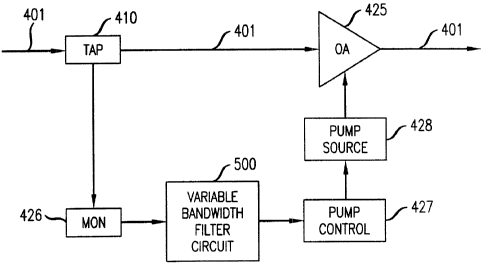
10 Briefly, an incoming optical signal 401 is tapped at optical tap 410 in a
well-known manner so that a first portion of the optical signal is routed to
optical
amplifier 425 and a second portion of the optical signal is routed to a signal
monitor 426. For example, tap 410 may comprise a so-called "9812" tap wherein
98%
of the optical signal power is supplied to optical amplifier 425 while 2% is
supplied to
optical monitor 426. Signal monitor 426 employs conventional circuitry and
techniques for measuring changes in signal power, i.e., input power to the
optical
amplifier, which is then used to control the amount of pump power for
effecting gain
control via pump control 427 and pump source 428. By way of example, signal
monitor 426 may include a photodetector or any other well-known, suitable
component that converts optical signal energy to a corresponding electrical
signal. In
the embodiment shown in FIG. 4, signal monitor 426 receives the tapped optical
signal from optical tap 410 and supplies an electrical signal to variable
bandwidth
filter circuit 500. The electrical signal output from signal monitor 426 is
therefore
used to facilitate the detection and measurement of signal power in the
corresponding
VdDM optical signal that is being supplied as input to optical amplifier 425.
According to the principles of the invention, variable bandwidth filter
circuit 500 can
be disposed between signal monitor 426 and pump control 427 to handle any
remnants that may exist in the incoming optical signal.
FIG. 5A shows one illustrative embodiment of variable bandwidth filter circuit
500 according to the principles of the invention. As shown, variable
CA 02331954 2001-O1-22
DEMCIN 11-2-1-3-1 11
bandwidth filter circuit 500 includes band splitter :> 10 for splitting input
signal 501
into its low frequency components for transmission in low pass section 51 l
and its
high frequency components for transmission in high pass section S 12. In the
present
embodiment, input signal 501 is an electrical signal that is supplied by
signal
monitor 426 (FIG. 4). Input signal 501 provides information about the measured
signal power corresponding to the optical signal that is tapped at a position
upstream
from optical amplifier 425 (FIG. 4). Low pass section 511 includes low
frequency
amplifier 520 while high pass section 512 includes high frequency amplifier
525
and switch 530. As will be described in more detail, high pass section 512 is
to "switched in" only for transient processing in response to the detection of
power
transients via transient detector 600. Band adder 535 combines the signal
components from low pass section 511 and high pass section S 12 to form output
signal 505. It will be apparent to those skilled in the art that band sputter
510, band
adder 535, switch 530, and low and high frequency amplifiers 520 and 525,
is respectively, can be implemented using conventional, well-known circuit
components, the operation of which is also well-known.
Band.splitter 510 operates in a conventional and well-known manner to split
input signal 501 into its fast and slow signal components. By way of example,
band
sputter ~ 10 can be any well-known filtering arrangement that serves as a low
pass
2o filter for directing the slow signal components, e.g., low frequency
components, via
low pass section 511 and as a high pass filter for directing the fast signal
components, e.g., high frequency components, via high pass section 512. The
slow
signal components in low pass section 511 are amplified by low frequency
amplifier
520 while the fast signal components in high pass section 512 are amplified by
high
25 frequency amplifier 525. Switch 530, which can be an analog switch, is
capable of
blocking the output of high frequency amplifier 5:?5 depending on the output
of
transient detector 600. In general, switch 530 either' operates in the open or
closed
position, wherein the closed position completes a circuit path to pass the
fast (high
frequency) signal components to band adder 535. In the open position, switch
530
3o prevents the fast (high frequency) signal components from reaching band
adder 535.
CA 02331954 2001-O1-22
DENK1N 11-2-1-3-i 12
More specifically, switch 530 is operated in the closed position when
transient detector 600 detects a power transient outside of acceptable
thresholds,
e.g., a large power transient caused by an actual transient event such as when
optical
channels are added/dropped in the WDM signal. In this way, both the high and
low
frequency components from high and Iow pass sections 512 and 511 respectively
are passed to band adder 535, which combines them to produce output signal
505.
Switch 530 is operated in the open position when transient detector 600 does
not
detect a power transient outside of acceptable thresholds, thereby blocking
the high
frequency signal components of input signal 501. Consequently, the high
frequency
to signal components are filtered from input signal 501 such that band adder
535 only
receives the low frequency signal components from low pass section 511 to
produce
output signal 505. Output signal 505 in this instance. would therefore be
considered
a filtered version of input signal 501. Advantageously, direct current (DC)
offsets
are minimized when switch 530 is opened or closed since DC is blocked for high
frequency amplifier 525. Output signal 505 from band adder 535 can then be
provided to subsequent gain control circuitry (e.g., pump control 427 in FIG.
4) to
effect appropriate control of the optical amplifier.
As will be described in more detail below with regard to FIG. 6A, transient
detector 600 is used to distinguish between power transients caused by actual
2o transient events and low level signal variations, such as the remnants
associated
with the power transients, so that appropriate filtering; can be performed by
variable
bandwidth filter circuit 500. In general, the filtering aspect of variable
bandwidth
filter circuit 500 provides bandwidth control for "capturing" power transients
caused
by actual transient events and for "ignoring" remnants of power transients or
other
unwanted signal variations with small signal amplitizdP so that subsequent
optical
amplifier control mechanisms can be controlled appropriately. Bandwidth
control is
achieved by operating variable bandwidth filter circuit: 500 with higher
bandwidth in
a first mode (e.g., when a transient event is detected) .and with lower
bandwidth in a
second mode (e.g., when a transient event is not detected).
CA 02331954 2001-O1-22
DENKIN 11-2-1-3-1 13
In particular, by passing both high and low frequency components of input
signal 501 when a transient event is detected by transient detector 600, the
bandwidth is effectively "opened" to capture both tlue high and low frequency
signal
components of the power transient. Sufr'icient bandwidth is important in this
case
because the shape and characteristics of the power transient need to be
preserved in
the signal so that subsequent control decisions, e.g., optical amplifier gain
control,
can be accurately performed. In contrast, by passing only the slowly varying
low
frequency components of input signal 501 when a power transient is not
detected by
transient detector 600, the bandwidth is ei~ectively "closed" or reduced so
that only
to slow variations in input signal SOl will be passed along. By blocking the
high
frequency components of input signal 501 in this latter case, any remnants of
a
previously occurring power transient or other low level signal variations,
e.g., noise
signals, will be substantially damped enough in magnitude so that they do not
disturb the network, e.g., trigger an undesirable gain control response. For
example,
depending ors system design parameters, it may be desirable to "knock down"
the
remnants from approximately 10% to approximately 1 %. In both cases, keeping
low frequency gain substantially the same, whether the high frequency
components
are being passed or blocked, ensures that offsets are kept to a minimum when
switching back and forth between the various outputs.
2o FIG. 7 further illustrates these bandwidth control aspects according to the
principles of the invention. A period of high banduridth, shown as shaded
portion
720, occurs around time lo to capture the full magnitude of power transient
716
(e.g., both the high and low frequency signal components). However, the period
of
high bandwidth is limited so that the remnants 717 arid 718 that occur at
subsequent
intervals of ~z are not captured as transient events. Consequently, pump
control
427 (FIG. 4) or other transient control circuitry would respond to power
transients
716 from the actual transient event while not being significantly affected by
remnants 717, 718 of the power transient. The filtering of remnants is an
important
advantage of the invention because remnants that would otherwise travel around
the
3o ring network could be amplified by subsequent nodes and eventually could
trigger
CA 02331954 2001-O1-22
DENKIhI i 1-2-1-3-1 14
undesirable responses in gain control circuitry, protection switching
circuitry, and so
on.
Although not shown in FIG. 5A, appropriate delays may be incorporated in
low frequency amplifier 520 or otherwise within low pass section 511 to
facilitate
parallel processing of the high and low frequency signal components of input
signal
501. For example, the delay through low frequency amplifier 510 could be
adjusted
to be substantially the same as the summed delay through high frequency
amplifier
520 and switch 530.
FIG. 5B shows another illustrative embodiment of a variable bandwidth
1o filter circuit according to the principles of the invention, shown here as
500'. As
shown, variable bandwidth filter circuit 500' includes delay element 560,
signal
processing element 570, transient detector 900, and analog switch 580. In one
embodiment, delay element 560 is an analog delay element and signal processing
element 570 is a low-pass filter, both of which can be implemented using
is conventional: circuitry well-known to those skilled in the art. It should
be noted that
the embodiments shown and described herein are :meant to be illustrative and
not
limiting in any manner. Accordingly, other suitable and well-known devices and
techniques will be apparent to those skilled in the art and may be substituted
consistent with the teachings of the invention.
2o Input signal 501 iS provided as input to delay element 560, signal
processing
element 570 (hereinafter low pass filter 570 in the present embodiment), and
transient detector 900. The detailed operation of transient detector 900 will
be
described below with reference to FIG. 6B. In general, the function of
transient
detector 900 is similar to that described for transient: detector 600 (FIG.
5A), i.e., to
25 distinguish power transients caused by actual transient events from
remnants or
other unwanted signal variations. In the embodiment shown in FIG. 5B,
transient
detector 900 determines when a power transient is caused by an actual
transient
event and causes an appropriate action by switch 580. As shown, analog switch
580
receives a delayed version of input signal 501, shown here as signal 561, as
well as
3o a processed or filtered version of input signal 501, shown here as signal
571. The
CA 02331954 2001-O1-22
DENKIN 11-2-1-3-1 15
delayed version 56I of input signal 501 includes both the high and low
frequency
components since no filtering occurs in this path. 13y contrast, filtered
version 571
of input signal 501 includes only low frequency components because of
filtering by
low pass filter 570.
Based on the output of transient detector 900, analog switch 580 selects
either the delayed version 561 of input signal 501 or the filtered version 571
of input
signal 501 depending on whether transient detector 900 detects an actual
transient
event. As in the preceding embodiment, when a power transient is detected,
analog
switch S80 selects the higher bandwidth, delayed version 561 of input signal
501 so
to that the full magnitude and characteristics of the power transient can be
captured.
By contrast, when a power transient is not detected, analog switch 580 selects
the
lower bandwidth, filtered version 571 of input signal 501. The signal selected
by
analog switch 580 is then provided as output signal SOS which is subsequently
processed by the gain control circuitry (e.g., pump control 427 in FIG. 4) to
effect
appropriate control of the optical amplifier.
In the preceding embodiments, either analog switch 530 or 580 can be
configured to include an additional control input: (not shown) for receiving a
separate control signal. By way of example only, the control input may be used
to
provide for software control of the system in one exemplary embodiment. Such
2o software control may be useful for operating analog switch 530 or 580 in a
particular state during startup procedures, during testing, and so on. In the
preceding embodiments, an optical delay element (not shown) may also be
incorporated between optical tap 410 and optical amplifier 425 (FIG. 4) to
provide
an additional predetermined amount of delay to compensate for processing
delays in
z5 variable bandwidth filter circuits 500 and 500', e.g., delays associated
with transient
detectors 600 and 900 (FIGS. 5A and 5B).
FIG. 6A shows an exemplary embodiment of transient detector 600
according to the principles of the invention. Briefly, transient detector 600
includes
a variable gain amplifier 610 for receiving input sil;nal 501, a gain
controller 611
3o coupled to variable gain amplifier 610, and a window discriminator 61 S
which
CA 02331954 2001-O1-22
DENKIN 11-2-1-3-1 16
receives, as one input, the amplified output signal 601 supplied by variable
gain
amplifier 610. Transient detector 600 further includes a signal threshold
generator
comprising reference voltage source 620, high limit controller 621, low limit
controller 623, and level controller 625 for establishing upper and lower
limits to
facilitate the detection of transients in input signal 501.
Flip-flop element 630 and delay element 631 operate in conjunction with
window discriminator 615 to effect the appropriatE: control over the selection
of
signals by switch 530 (see FIG. 5A). The basic principles of operation of
variable
gain amplifiers, gain controllers (e.g., operational amplifier-based
circuits), window
to discriminators, voltage limit controllers, and flip-flops are well-known to
those
skilled in the art and will not be described in detail here for sake of
brevity. Instead,
the use of these well-known circuit components will'. be described in terms of
their
functions that are relevant to practicing the invention. It should also be
noted that
this embodiment is meant to be illustrative only and not limiting. As such,
various
modifications and substitutions will be apparent to l:hose skilled in the art
and are
contemplated by the teachings herein.
In the, embodiment shown in FIG. 6A, high limit controller 621 and low
limit controller 623 serve as voltage sources that are derived from reference
voltage
source 620. In particular, the output of reference voltage source 620 is
provided as
2o input-to both high limit controller 621 and low limit controller 623.
Responsive to
reference voltage source 620, high limit controller 6:Z 1 outputs a voltage
level that
represents an upper limit or upper threshold 622 for input signal 501, while
low
limit controller 623 outputs a voltage level that represents a lower limit or
lower
threshold 624 for input signal 501. It should be noted that the prescribed
values for
upper and lower thresholds 622 and 624 respectively are a matter of design
choice.
For example, one factor affecting the selection of appropriate values could be
the
number of optical channels in the WDM system since adding/dropping channels in
a
system carrying a fewer number of channels could have a greater impact than in
a
system with a greater number of channels, e.g., adding;/dropping 1 channel
from a 4-
34 channel system versus adding/dropping 1 channel from an ~0-channel system.
In
CA 02331954 2001-O1-22
DE1VKIN 11-2-1-3-1 17
principle, selection of appropriate upper and lower thresholds 622 and 624
will
ensure that acceptable thresholds are in place to detect transient events of
varying
magnitude.
As will be described in more detail below, both upper and lower thresholds
622 and 624, respectively, are provided as inputs to window discriminator 615.
Upper and lower thresholds 622 and 624, respectively, are also provided as
inputs to
level controller 625, which supplies an output signal 626 that is voltage
constrained
between the outputs of high and low limit controllers 621 and 623,
respectively.
Output signal 626 is coupled to gain controller 61 l, which is used to control
the gain
to of variable gain amplifier 610.
When input signal 501 is not changing, variable gain amplifier 610 is
responsive to gain controller 6 l 1 and operates at a gain such that its
output signal
601 equals output signal 626, which is voltage constrained between upper and
lower
thresholds 622 and 624, respectively. In one exemplary embodiment, gain
controller 611 may comprise an operational ampli~Eer coupled by an appropriate
resistive element or elements between level controller 625 and variable gain
amplifier 610. Other gain control implementations will be apparent to those
skilled
in the art.
As shown in FIG. 6A, window discriminator 615 receives three inputs, those
2o being upper threshold voltage level 622, lower threshold voltage level 624,
and
variable gain amplifier output signal 601. According to well-known principles
of
operation, window discriminator 61 S determines whcaher output signal 601
remains
within upper and lower threshold voltage levels ~522 and 624 and produces a
resultant logic output to flip-flop element 630. ~~Vhen input signal 501 is
not
changing, window discriminator 61 S would indicate that output signal 601 is
within
the upper and lower thresholds 622 and 624 (e.g., no transient event) because
output
signal 601 in this case would equal output signal Ei26 from level controller
625.
When input signal 501 is changing, the operation of transient detector 600
will be
better understood in view of the following two examples.
3o EXAMPLE 1
CA 02331954 2001-O1-22
DENKIN 11-2-1-3-1 1g
When there is a sudden large change in input signal SOl, output signal 601
of variable gain amplifier 610 changes to follow input signal SOl given the
typical
operating characteristics of a variable gain amplifier. As such, output signal
601
will now be outside the limits established by upper and lower thresholds 622
and
624, i.e., either exceeding upper threshold 622 or falling below lower
threshold 624,
as determined by window discriminator 61 S according to well-known principles
of
operation. When output signal 601 is outside the; limits set by upper and
lower
thresholds 622 and 624, i.e., indicating a transient event, the logic output
of window
discriminator 61S will then drive operation of flip-flop element 630 which in
turn
lo drives operation of switch 530. As previously described, switch S30 will
operate to
allow both the high and low frequency components of input signal SO1 to be
passed
to band adder 535 (FIG. 5A). In this way, the bandwidth is eflFectively
"opened" so
that the full magnitude, shape, etc. of the power traJlsient in input signal
501 can be
captured for subsequent gain control processing.
1 s As shown, the output from window discriminator 61 S is also provided to
delay element 631 which is further coupled to fliip-flop element 630. Flip-
flop
element 630 is therefore automatically reset following the delay provided by
delay
element 631. Resetting flip-flop element 630 after the delay will in turn
cause
switch S30 to change states, effectively "closing" the bandwidth and blocking
the
20 high frequency components as previously described for FIG. SA. The amount
of
delay provided by delay element 631 is a matter of design choice, e.g.,
ideally less
than one round trip around a WDM ring network.
Gain controller 611 adjusts the gain of variable gain amplifier 610 with a
time constant l. After several time-constants, output signal 601 will again
equal
25 output signal 626 (supplied by level controller 625), which will be noted
by window
discriminator 61 S. It should be noted that this time; constant is much
shorter than
the amount of delay associated with delay element 631.
EXAMPLE 2
In this example, assume the change in input signal SO1 is somewhat smaller
3o so that output signal 601 from variable gain amplifier 610 does not exceed
or fall
CA 02331954 2001-O1-22
DENKIN 11-2-1-3-1 19
below the upper or lower thresholds 622 and 624, respectively. In this case,
the
logic output of window discriminator 615 will not trigger flip-flop element
630. All
other circuits will operate as described in the preceding example.
FIG. 6B shows another illustrative embodiment of a transient detector
according to the principles of the invention, shown here as transient detector
900.
Briefly, transient detector 900 includes two parallel circuit paths, each path
including one of sample and hold circuits 930 and 935, two of multiplying
amplifiers 940, 945, 950, and 955, and one of window comparators 960 and 965.
As will be described in more detail below, the two parallel circuit paths
support the
to same processing functions except that processing in one of the circuit
paths is
delayed as compared to the other circuit path. Sannple generator 910 and
sample
delay element 920 supply pulses and delayed pulses. to the appropriate sample
and
hold circuits 930 and 935 according to well-known principles of operation.
Transient detector 900 further includes a logical OR element 970 for receiving
logic
inputs from window comparators 960 and 965, flip-flop logic element 975 for
receiving the output from logical OR element 970, and delay element 980, the
operation of which will be described in more detail below. The circuitry anri
operation of sample and hold circuits, multiplying amplifiers, window
comparators,
logical OR elements, and flip-flops are well-known to those skilled in the art
and
2o will not be described in detail here for sake of brevity. It should also be
noted that
this embodiment is meant to be illustrative only and not limiting in any way.
In operation, sample generator 910 generates .a continuous series of pulses to
sample and hold circuit 930. When one of those pulses arnves at sample and
hold
circuit 930, the current value of input signal 501 is held constant until the
next
sample pulse and delivered to each of multiplying amplifiers 940 and 950.
Multiplying amplifier 940 multiplies the current v~~lue of input signal 501 by
a
predetermined multiplier value (A) 942 to produce an upper threshold value
941.
This upper threshold value 941 represents an upper threshold for changes in
input
signal 501. In one embodiment, multiplier value (A) 942 has a value greater
than 1.
3o Similarly, multiplying amplifier 950 multiplies the current value of input
signal 501
CA 02331954 2001-O1-22
DENKIN II-2-I-3-I 20
by a predetermined multiplier value (B) 952 to produce a lower threshold value
951.
As such, this. lower threshold value 951 represents a, lower threshold for
changes in
input signal 501. In one embodiment, multiplier vahae (B) 952 has a value less
than
1.
As with the embodiment shown and described in FIG. 6A, it should be noted
that the predetermined values for multiplier values (A and B) 942 and 952 are
a
matter of design choice and will depend on the aforementioned factors, e.g.,
number
of optical channels in the WDM system, and so on.
Continuing with the embodiment shown in FIG. 6B; window comparator
to 960 receives three inputs, those being input signal 501, upper threshold
value 941,
and lower threshold value 951. While input signal 501 may be constantly
changing,
the upper and lower threshold values 941 and 951 only change when a new sample
pulse arrives at sample and hold circuit 930. When the value of input signal
501
moves outside the limits established by upper and lower threshold values 941
and
95 l, the output of window comparator 960 conveys that information as a logic
input
to logical OR element 970. Thus, when input signal. 501 changes to a value
that is
outside the Iixnits set by upper and lower threshold values 941 and 951, i.e.,
indicating a transient event, the output of logical OR element 970 activates
flip-flop
element 975. The output of flip-flop element 975 activates analog switch 580
(FIG.
2o SB), thereby opening the bandwidth for a period covering the duration of
the initial
transient, but Less than the time for the remnants to travel around the ring,
e.g.,
Di (see FIGS. 3 and 7).
As shown, flip-flop element 975 receives inputs from logical OR element
970 and delay element 980 and provides an output to analog switch 580 (FIG.
5B).
Flip-flop element 975 is automatically reset following a delay determined by
delay
element 980. Again, the amount of delay provided by delay element 980 is a
matter
of design choice, e.g., ideally less than one round trip around a WDM ring
network.
According to another aspect of the invention, the parallel circuit path
including sample and hold circuit 935, multiplying amplifiers 945 and 955, and
3o window comparator 965 are used to ensure that a tra.r~sient event is not
missed. For
CA 02331954 2001-O1-22
DENK1N 11-2-1-3-1 21
example, a transient event might be missed if iinput signal 501 changes (i.e.,
transient event) at the precise time when the sample pulse selects new upper
and
lower threshold values 941 and 951. In operation, sample and hold circuit 935,
multiplying amplifiers 945 and 955, multiplier valuca (C and D) 947 and 957,
upper
and lower threshold values 946 and 956, and window comparator 965 perform
functions similar to those described above and will not be repeated here for
sake of
brevity. Because the sample pulse for this parallel circuit path is delayed by
sample
delay 920, the limits set by upper and lower threshold values 946 and 956 for
window comparator 965 change at a different time than the limits set by upper
and
to lower threshold values 941 and 951 for window comparator 960. Consequently,
by
adding the second parallel circuit path and logically "OR"ing the outputs of
each
path, all transient events will therefore be detected regardless of timing
since the
upper and lower threshold values 941 and 951 will not be changing at the same
time
as upper and lower threshold values 946 and 956.
FIG. 7 shows the characteristics of a signal after being processed by either
variable bandwidth filter circuit 500 (FIG. 5A) or :500' (FIG. 5B) according
to the
principles of the invention (compare to the unprocessed signal in FIG. 3). As
shown
in FIG. 7, the power transient at time 'to is shown to occur when a signal
drops from
a first power level 715 to a second power level 716 in response to a
particular event
or condition. This power transient therefore corresponds to the initial
transient
event. Because the duration of maximum bandwidth (shaded portion 720), only
occurs around time io when the transient event occurs, remnants 717 and 718
are
therefore substantially filtered out according to the principles of the
invention.
As previously described, the filtering performed according to the principles
of the invention ensures that the bandwidth is "opened" at time io to capture
the full
magnitude, shape, etc. of the power transient, but "closed" after time zo so
that
remnants 717 and 718 are filtered out, "knocked down", or substantially
suppressed
enough in magnitude so that they do not disturb transmission in the ring
network. In
fact, remnants 717 and 718 become progressively weaker as they travel around
the
3o ring since they are no longer strong enough to trigger a transient event at
subsequent
CA 02331954 2001-O1-22
° DENKIN 11-2-1-3-1 22
nodes which would otherwise lead to undesirable amplification of the remnants.
Accordingly, pump control 427 (FIG. 4) receives a signal having
characteristics as
shown in FIG. 7, i.e., preservation of power transient and "knocked down"
remnants. Appropriate gain control can then be effected for optical amplifier
425 in
response to the power transient while unwanted or undesirable responses to
remnants or other noise in the signal are substantially reduced.
Other variations or modifications to the embodiments shown and described
herein will be apparent to those skilled in the art consistent with the
teachings of the
invention. For example, control of the bandwidth (i.e., opening and closing)
to performed by analog switch 580 and low pass filter 570 (FIG. 5B) could be
performed by a sample and hold circuit (not shown). For example, the sample
and
hold circuit would track during the shaded interval '720 (see FIG. 7) and be
in a hold
pattern at the end of the interval. In this manner, input signal 501 would be
updated
whenever a transient occurs. Periodic updates could also follow at times that
greatly
exceed Di, i.e., the time for a remnant to travel completely around the ring.
For this
case, transient detector 900 would not require flip-flop element 975 and the
associated circuitry. An optical delay element (not shown) placed in the
transmission path would also permit the control signal to change at the same
time as
when the number of channels changes, i.e., the transient event.
~Companding amplifiers could also be used where nonlinear detection of
transients is desired. In such cases, the system could, for example, be made
more
responsive to losses of power rather than to increases in power. A tunable
filter (not
shown) could also be used according to the principles of the invention. In
this case,
an important design factor would relate to the response characteristics of the
tunable
filter for changing bandwidth. For example, the tunable filter should ideally
operate
such that the bandwidth can be increased, i.e., opened, to a maximum value in
less
time than it takes for a power transient to drive the output to unacceptable
levels.
Furthermore, trade-offs~~can be made as a matter of design choice as to
whether the circuitry responds to percentage changes or absolute changes, both
of
o which result in different amounts of control activity.
CA 02331954 2001-O1-22
DENKIN i 1-2-1-3-1 23
The foregoing is merely illustrative of the principles of the invention. Those
skilled in the art will be able to devise numerous arrangements, which,
although not
explicitly shown or described herein, nevertheless embody those principles
that are
within the scope of the invention. For example, although the illustrative
embodiments were described in the context of optical amplifier control in WDM
ring networks, the principles of the invention may be employed with any
control
system in which there is a desired response to large signals accompanied by a
need
to limit or suppress undesirable responses to small signal variations.