Note: Descriptions are shown in the official language in which they were submitted.
CA 02332405 2001-02-06
f
r
SPECIFICATION
TITLE OF T INVENTION
Communication System
HACKGR UNj? OF THE INVENTIaN
1. Field of the Invention:
The present invention relates to a communication system
for transmission/reception of a digital signal through
modulation of its carrier wave and demodulation of the
- modulated signal.
113 2. Description of the Prior Art:
Digital communication systems have been used in various
fields. Particularly, digital video signal transmission
techniques have been improved remarkably.
Among them is a digital TV signal transmission method.
So far, such digital TV signal transmission system are in
particular use for e.g. transmission between TV stations.
They will soon be utilized for terrestrial and/or satellite
broadcast service in every country of the world.
The TV broadcast systems including HDTV. PCM music, FAX,
and other information service are now demanded to increase
desired data in quantity and quality for satisfying millions
of sophisticated viewers. In particular, the data has to be
increased in a given bandwidth of frequency allocated for TV
broadcast service. The data to be transmitted is always
abundant and provided as much as handled with up-to-date
techniques of the time. It is ideal to modify or change the
existing signal transmission system corresponding to an
1
CA 02332405 2001-02-06
increase in the data amount with time.
However, the TV broadcast service is a public business
and cannot go further without considering the interests aid
benefits of viewers. It is essential to have any new service
5 appreciable with existing TV receivers and displays. More
particularly, the compatibility of a system is much desired
for providing both old and now services simultaneously or one
new service which can be interceyted by either of the
existing and advanced receivers.
10 It is understood that any new digital TV broadcast
system to be introduced has to be arranged for data extension
in order to respond to future demands and technological
advantages and also, for compatible action to allow the
existing receivers to receive transmissions.
15 The expansion capability and compatible performance of
prior art digital TV system will be explained.
A digital satellite TV system is known in which NTSC TV
signals compressed to an about 6 Mbps are multiplexed by time
division modulation of 4 PSK and transmitted on 4 to 20
20 channels while HDTV signals are carried on a single channel.
:~.nother digital HDTV system is provided in which HDTV video
data compressed to as small as 15 Mbps are transmitted or. a
16 or 32 pAM signal through ground stations.
Such a known satellite system permits HDTV signals to be
25 carried on one channel by a conventional manner, thus
occupying a band of frequencies equivalent to same channels
of ~TSC signals. This causes the corresponding NTSC channels
2
CA 02332405 2001-02-06
to be unavailable during transmission of the HDTV signal.
also, the compatibility between NTSC and HDTV receivers or
displays is hardly concerned and data expansion capability
needed for matching a future advanced mode is utterly
disregarded.
Such a common terrestrial IiDTV system offers an ATV
service on conventional 16 or 32 QAM signals without any
modification. in any analogue TV broadcast service, there are
developed a Iot of signal attenuating or shadow regions
10 within its service area due to structural obstacles,
geographical inconveniences, or signal interference from a
neighbor station. When the TV signal is an analogue form, it
can be intercepted more or less at such signal attenuating
regions although ita reproduced picture is Iow in quaiity~. if
15 TV signal is a digital form, it can rarely bye reproduced at
an acceptable level within the regions. This disadvantage is
critically hostile to the development of any digital TV
system.
This problem is caused due to the fact that the
20 conventional modulation systems such QAM arrange the signal
points at constant intervals. There have been no such systems
that can change or modulate the arrangement of signal points.
S~'S,j~iARY' OF THE INVEVTI N
25 It is an object of the present invention, for solving
the foregoing disadvantages, to provide a communication
system arranged for compatible use for both the existing rTSC
3
CA 02332405 2001-02-06
and introducing HDT4 broadcast services, particularly via
satellite and also, for minimizing signal attenuating or
shadow regions of its service area on the grounds.
A communication system according to the present
invention intentionally varies signal points, which used to
be disposed at uniform intervals, to perform the signal
transmission/reception. For example, if applied to a QAM
signal, the communication system comprises two major
sections: a transmitter having a signal input circuit, a
10 modulator circuit for producing m numbers of signal points,
in a signal vector Field through modulation of a plurality of
out-of-phase carrier waves using an input signal supplied
from the input circuit, and a transmitter circuit for
transmitting a resultant modulated signal; and a receiver
15 having an input circuit for receiving the modulated signal,
a demodulator circuit for demodulating one-bit signal points
of a qA'~i carrier wave, and an output circuit.
In operation, the input signal containing a first data
stream of n values and a second data stream is fed to the
20 modulator circuit of the transmitter where a modified m-bit
1("~M carrier wave is produced representing m signal points in
a vector field. The m signal points are divided into n signal
point groups to which the n values of the first data stream
are assigned respectively. Also, data of the secona oata
25 stream are assigned to m%r signal points or sub groups of
each signal point group. Then, a resultant transmission
signal is transmitted from the transr.~itter circuit.
4
CA 02332405 2001-02-06
Similarly, a third data stream can be propagated.
At the p-bit demodulator circuit, p>m, of the receiver,
the first data stream of the transmission signal is first
demodulated through dividing p signal points in a signal
space diagram into n signal point groups. Then, the second
data stream is demodulated through assigning p/n values to
p/n signal points of each corresponding signal point group
for reconstruction of both the first and second data streams.
If the receiver is at P=n, the n signal point groups are
10 reclaimed and assigned the n values for demodulation and
reconstruction of the first data stream.
Upon receiving the same transmission signal from the
transmitter, a receiver equipped with a large sized antenna
and capable of large-data modulation can reproduce both the
16 first and second data streams. A receiver equipped with a
small sized antenna and capable of small-data modulation can
reproduce the first data stream only. Accordingly, the
compatibility of the signal transmission system will be
ensured. When the first data stream is an NTSC TV signal or
20 low frequency band component of anI~TV signal and the second
data stream is a high frequency band component of the HDTV
signal, the small-data modulation receiver can reconstruct
the NTSC TV signal and the large-data modulation receiver can
reconstruct the ITV signal. As understood, a digital
25 NTSC/HDT'~~ simultaneously broadcast service will be feasible
using the compatibility oz the signal transmission system of
the present invention.
5
CA 02332405 2001-02-06
More specifically, the communication system of the
present invention comprises; a transmitter having a signal
input circuit, a modulator circuit for producing m signal
points, in a signal vector field through modulation of a
5 plurality-of out-of-phase carrier waves using an input signal
supplied from the input, and a transmitter circuit for
transmitting a resultant modulated signal, in which the main
procedure includes receiving an input signal containing a
first data stream of n values and a second data stream,
10 dividing the m signal points of tire signal into n signal
point groups, assignir:g the n values of the first data stream
to the n signal point groups respectively, assigning data of
tha second data stream to the signal points of each signal
point group respectively, and transmitting the resultant
15 modulated signal; and a receiver having an input circuit for
receiving the modulated signal, a demodulator circuit for
demodulating p signal points of a 61AM carrier wave, and an
output circuit, in which the main procedure includes dividing
the p signal points into n signal point groups, demodulating
20 the first data stream of which n values are assigned to the
n Signal point groups respectively, and demodulating the
secor_d data stream of which p/n values are assigned to p/n
signal points of each signal point group respectively. For
example, a transmitter 1 produces a modified m-bit ~i signal
2~~ of which first, second, and third data streams, each carrying
n values, are assigned to relevant signal point groups with
a modulator 4. The signal can be intercepted and reproduced
6
CA 02332405 2001-02-06
the first data stream only by a first receiver 23, both the
first and second data streams by a second receiver 33, and
all the first, second, and third streams by a third receiver
43.
5 More particularly, a receiver capable of demodulation of
n-bit data can reproduce n bits from a multiple-bit modulated
carrier wave carrying an m-bit data where m>n, thus allowing
the communication system to have compatibility and capability
of future extension. Also, a mufti-level signal transmission
10 will be possible by shifting the signal points of Q.AM so that
a nearest signal point to the origin point of I-axis and Q-
axis coordinates is spaced of from the origin where f is the
distance of the nearest point from each axis and n is more
than 1.
15 Accordingly, a compatible digital satellite broadcast
service for both the NTSC and HBTV systems will be feasible
when the first data stream carries an NTSC signal and the
second data stream carries a difference signtsl between NTSC
and HDTV. Hence, the capability of corresponding to an
20 increase in the data amount to be transmitted will be
ensured. Also, at the ground, its service area will be
increased while signal attenuating areas are decreased.
RItIRi' DESCRIPT ON OF THE DRAWINGS
25 Fig. 1 is a schematic view of the entire arrangement of
a signal transmission system showing a first embodiment of
the present invention;
7
CA 02332405 2001-02-06
..z. . ...
rig. 2 is a block diagram of a transmitter of the first
embodiment;
Fig. 3 is a vector diagram showing a transmission signal
of the first embodiment;
5 Fig. 4 is a vector diagram showing a transmission signal
of the first embodiment;
Fig. 5 is a view showing an assignment of binary codes
to signal points according to the first embodiment;
Fig. 6 is a view showing an assignment of binary codes
to signal point groups according to the first embodiment;
Fig. 7 is a view showing an assignment of binary codes
to signal points in each signal point group according to the
first embodiment;
Fig. B is a view showing another assignment of binary
15 codes to signal point groups and their signal points
according to the first embodiment;
Fig. 9 is a view showing threshold values of the signal
point groups according to the first Qmbodiment;
Fig. 10 is a vector diagram of a modified 16 eA.M signal
of the first embodiment;
Fig. 11 is a graphic diagram showing the relation
between antenna radius rZ and transmission energy ratio n
according to the first embodiment;
Fig. 12 is a view stowing the signal points of a
modified 64 QAM signal of the first embodiment;
Fig. 13 is a graphic diagram showing the relation
betwean anter_na radius r3 and transmission energy ratio n
8
CA 02332405 2001-02-06
according to the first embodiment;
Fig. 14 is a vector diagram showing signal point groups
and their signal points of the modified 6:1 QA~'H signal of the
first embodiment;
Fig. 15 ie an explanatory view showing the relation
between Al and A' of the modif led 64 QAI'I s ignal of the f l rst
embodiment;
Fig. 16 is a graph diagram showing the relation between
antenna radius r2, r3 and transmission energy ratio n16~ n~
respectively according to the first embodiment;
Fig. 17 is a block diagram of a digital transmitter of
the first embodiment;
Fig. 18 is a signal space diagram of a 4 PSK modulated
signal of the first embodiment;
Fig. 19 is a block diagram of a first receiver of the
first embodiment;
Fig. 20 is a signal space diagram of a 4 PSK modulated
signal of the first embodiment;
Fig. 21 is a block diagram of a second receiver of the
first embodiment;
Fig. 22 is a vector diagram of a modified 16 Q.AM signal
of the first embodiment;
Fig. 23 is a vector diagram of a modified 64 QAM signal
of the first embodiment;
Fig. 24 is a flow chart showing an action of the first
embodiment;
Figs. 25(a) and 25(b) are vector diagrams showing an B
9
CA 02332405 2001-02-06
and a 16 QAM signal of the first embodiment respectively;
Fig. 26 is a block diagram of a third receiver of the
first embodiment;
Fig. 2~ is a view showing signal points of the modified
64 qAM signal of the first embodiment.;
Fig. 28 is a flow chart showing another action of the
first embodiment;
Fig. 29 is a schematic view of the entire arrangement o~
a signal transmission system showing a third embodiment of
10 the present invention;
Fig. 30 is a block diegram of a first video encoder of
the third embodiment;
Fig. 31 is a block diagram of a first ~rideo decoder of
the third embodiment;
Fig. 32 is a block diagram of a second video decoder of
the third embodiment;
Fig 33 is a block diagram of a third video decoder of
the third embodiment;
Fig. 34 is an explanatory view showing a time
20 multiplexing of D1, DZ, and D3 signals according to the third
embodiment;
Fig. 35 is an explanatory view showing another time
multiplexing of the D1, DZ, and D3 signals according to the
third embodiment;
25 Fig. 36 is an explanatory view showing a further time
multiplexing of the D1, DZ, and D3 signals according to the
third embodiment;
CA 02332405 2001-02-06
Fig. 37 is a schematic view of the entire arrangement of
a signal transmission system showing a fourth embodiment of
the present invention;
Fig. 38 is a vector diagram of a modified 16 QAM signal
of the third embodiment;
Fig. 39 is a vector diagram of the modified 16 QA:'H
signal of the third embodiment;
Fig. 40 is a vector diagram of a modified 64 6iAM signal
of the third embodiment;
10 Fig. 41 is a diagram of assignment of data components on
a time base according to the third embodiment;
Fig. 42 is a diagram of assignment of data components on
a time base in TDMA action according to the third embodiment;
Fig. 43 is a block diagram of a carrier reproducing
15 circuit of the third embodiment;
Fig. 44 is a diagram showing the principle of carrier
wave reproduction according to the third embodiment;
Fig. 45 is a block diagram of a carrier reproducing
circuit for reverse modulation of the third embodiment;
20 Fig. 46 is a diagram showing an assignment of signal
points of the 16 WAM signal of the third embodiment;
Fig. 47 is a diagram showing an assignment of signal
points of the 64 QAM signal of the third embodiment;
Fig. 48 is a block diagram of a carrier reproducing
25 circuit for lfix multiplication of the third embodiment;
Fig. 49 is an explanatory view showing a time
multiplexing of D,~l, Ddl, Dy2, D~, DV3, arid D~ signals according
11
CA 02332405 2001-02-06
to the third embodiment;
Fig. 50 is an explsnatory view showing a TD;~.A time
multiplexing of Dyl, Dd" Dy2, D~, D~, and D~ signals according
to the third embodiment;
5 Fig. 51 is an explanatory view showing another TDMA time
multiplexing of the DYl, D81, Due, Due, IlY3, and D~ signals
according to the third embodiment;
Fig. 52 is a diagram showing a signal interference
region in a known transmission method according to the fourth
10 embodiment;
Fig. 53 is a diagram showing signal interference regions
in a multi-level signal transmission method according to the
fourth embodiment;
Fig. 54 is a diagram showing signal attenuating regions
15 in the known transmission method according to the fourth
embodiment;
Fig. 55 is a diagram showing signal attenuating regions
in the multi-level signal transmission method according to
the fourth embodiment;
20 Fig. 56 is a diagram showing a signal interference
region between two digital TV stations according to the
fourth embodiment;
Fig. 57 is a diagram showing an assignment of sigrial
points of a modified 4 ASR signal of the fifth embodiment;
25 Fig. ~8 is a diagram showing another assignment of
signal points of the modified 4 ASK signal cf the fifth
embodiment;
12
CA 02332405 2001-02-06
. - . , _ . . ~ . _ , 't-,~'_ -'-';-.'- . . - . : : _ _ .
Figs. 59(a) and 59(b) are diagrams showing assignment of
signal points of the modified 4 ASK signal of the fifth
embodiment;
Fig. 60 is a diagram showing another aesignmert of
signal points of the modified 4 ASK signal of the fifth
embodiment when the C/N rate is low;
Fig. 61 is a block diagram of a transmitter of the fifth
embodiment;
Figs. 62(a) and 62(b) are diagrams showing frequency
distribution profiles of an ASK modulated signal of the fifth
embodiment;
Fig. 63 is a block diagram of a receiver of the fifth
embodiment;
Fig. 64 is a block diagram of a video signal transmitter
of the fifth embodiment;
Fig. 65 is a block diagram of a T'V receiver of the fifth
embodiment;
Fig. 66 is a block diagram of another iV receiver of the
fifth embodiment;
Fig. 67 is a block diagram of a satellite-to-ground TV
receiver ef the fifth embodiment;
Fig. 68 is a diagram showing an assignment of signal
points of an 8 ASK signal of the fifth embodiment;
F'ig. 6g is a block diagram of a video encoder of the
fifth embodiment;
Fig. 70 is a block diagram of a video encoder of the
fifth embodiment containing one d=eider circuit;
13
CA 02332405 2001-02-06
. . . . . . _ . _ . F: .. '~~.~'_ '_' a'." . . . . z .
Fig. 71 is a block diagram of a video decoder of the
fifth embodiment;
Fig. 72 is a block diagram of a ~~ideo decoder o~ the
fifth embodiment containing one mixer circuit;
Fig. 73 is a diagram showing a time assignment of data.
components of a transmission signal according to the fifth
embodiment;
Fig. 74(a) is a block diagram of a video decoder of the
fifth embodiment;
Fig. 74(b) is a diagram showing another time assignment
of data components of the transmission signal according to
the fifth embodiment;
Fig. 75 is a diagram showing a time assignment of data
components of a transmission signal according to the fifth.
embodiment;
Fig. 76 is a diagram showing a time assignment of data
components of a transmission signal according to the fifth
embodiment;
Fig. 77 is a diagram showing a time assignment of data
components of a transmission signal according to the fifth
embodiment;
Fig. 78 is a block diagram of a video decoder cf the
fifth embodiment;
Fig. 79 ie a diagram showing a time assignment of data
components of a three-level transmission signal according to
the fifth embodiment;
Fig. BO is a block diagrac: of another video decoder of
14
CA 02332405 2001-02-06
._.. .._. . f'_. 'z:~_ '~~~o~F- . ._z_ . ,. "..
the fifth embodiment;
Fig. 8i is a diagram showing a time assignment of da!a
components of a transmission signal according to the fifth
embodiment;
Fig. 82 is a block diagram of a video decoder for D,
signal of the fifth embodiment;
Fig. 83 is a graphic diagram showing the relation
between frequency and time of a frequency modulated signal
according to the fifth embodiment;
Fig. 84 is a block diagram of a magnetic record/playback
apparatus of the fifth embodiment;
Fig. 85 is a graphic diagram showing the relation
between C/N and level according to the second embodiment;
Fig. 86 is a graphic diagram showing the relation
between C/N and transmission distance according to the second
embodiment;
Fig. 87 is a block diagram of a transmission of the
second embodiment;
Fig. 88 is a block diagram of a receiver of the second
embodiment;
Fig. 89 is a graphic diagram showing the relation
between C/N and error rate according to the second
embodiment;
Fig. 90 is a diagram showing signal attenuating regions
in the three-level transmission of the fifth embodiment;
Fig. 91 is a diagram showing signal attenuating regions
in the four-level transmission of a sixth embodiment;
CA 02332405 2001-02-06
- ~ ~,_ -_-;~-__
Fig. 92 is a diagram shoeing the four-level transmission
of the eixth embodiment;
Fig. 93 is a block diagram of a divider of the sixth
embodiment;
Fig. 94 is a block diagram of a mixer of the sixth
embodiment;
Fig. 95 is a diagram showing ar_other four-Ievel
transmission of the sixth embodiment;
Fig. 96 is a view of signal propagation of a known
digital TV broadcast system;
Fig. 97 is a view of signal propagation of a digital TV
broadcast slstem according to the sixth embodiment;
Fig. 9B is a diagram showing a four-level transmission
of the sixth embodiment;
Fig. 99 is a vector diagram of a 16 SRQAM signal of the
third embodiment;
Fig. 100 is a vector diagram of a 32 SRQAM signal of the
third embodiment;
Fig. I01 is a graphic diagram showing the relation
between C/N and error rate according to the third embodiment;
Fig. 102 is a graphic diagram showing the relation
between C/h and error rate according to the third embodiment;
fig. 103 is a graphic diagram showing tile relation
between shift distance n and C/N needed for transmission
according to the third embodiment;
Fig. 104 is a graphic diagram showing the relation
between shift distance n and C/N needed for transmission
18
CA 02332405 2001-02-06
according to the third embodiment;
Fig. 105 is a graphic diagram showing the relation
between signal level and distance from a transmitter antenna
in terrestrial broadcast service according to the third
embodiment;
Fig. 106 is a diagram showing a service area of the 32
SRQAM signal of the third embodiment;
Fig. 107 is a diagram showing a service area of the 32
SRQAM signal of the third embodiment;
Fig. 108 is a diagram showing a frequency distribution
profile of a TV signal of the third embcdiment;
Fig. 109 is a diagram showing a time assignment of the
TV signal of the third embodiment;
Fig. 110 is a diagram showing a principle of C-CDM of
the third embodiment;
Fig. 111 is a view showing an assignment of codes
according to the third embodiment;
Fig. 112 is a view showing an assignment of an extended
38 C~.A.~f according to the third embodiment;
Fig. 113 is a view showing a frequency assignment of a
modulation signal according to the fifth embodiment;
Fig. 114 is a block diagram showing a magnetic
recording/piayback apparatus according tc the fifth
embodiment;
Fig. 115 is a block diagram showing a
transmitter/receiver of a portable telephone according to the
eighth embodiment;
17
CA 02332405 2001-02-06
..._ . _._ ,_..
~ _, - ~_ ~';,.
Fig. 116 is a block diagram showing base stations
according to the eighth embodiment;
Fig. 1L'7 is a view illustrating communication capacities
and traffic distribution of a conventional system;
Fig. 118 is a view illustrating communication capacities
and traffic distribution according to the eighth embodiment;
Fig. 119(x) is a diagram showing a time slot assignment
of a conventional system;
Fig. 119(b) is a diagram showing a time slot assignment
according to the eighth embodiment;
Fig. 120(x) is a diagram showing a time slot assignment
of a conventional TDMA system;
Fig. 120(b) ie a diagram showing a time slot assignment
according to a TDMA system of the eighth embodiment;
Fig. 121 is a block diagram showing a one-level
transmitter/receiver according to the eighth embodiment;
Fig. 122 is a block diagram showing a two-level
transmitter/receiver according to the eighth embodiment;
Fig. 123 is a block diagram showing an OFDM type
transmitter/receiver according to the ninth embodiment;
Fig. 124 is a view illustre,ting a principle of the OFDM
system according to the ninth embodiment;
Fig. 125(a) is a view showing a frequency assignment of
a modulation signal of a conventional system;
Fig. 125(b) is a view showing a frequency assignment of
a modulation signal according to the ninth embodiment;
Fig. 126(x) is a view showing a frequency assignment of
18
CA 02332405 2001-02-06
. . : _ - _ ', _ - . ~ _ -~'~ r-.= ~ cw-o-: ~ .. . . . - _ . . _ . . _ .
a transmission signal of the ninth embodiment;
Fig. 126(b) is a view showing a frequency assignment of
a receiving signal according to the ninth embodiment;
Fig. 127 is a block diagram showing a
transmitter/receiver according to the ninth embodiment;
Fig. 128 is a block diagram showing a Trellis encoder
according to the fifth embodiment;
Fig. 129 is a view showing a time assignment of
effective symbol periods and guard intervals according to the
ninth embodiment;
Fig. 130 is a graphic diagram showing a relation between
C/N rate and error rate according to the ninth embodiment;
Fig. 131 is a block diagram showing a magnetic
recording; playback apparatus according to the fifth
embodiment;
Fig. 132 is a view si~.owing a recording format of track
on the magnetic tape and a travelling of a head;
Fig. 133 is a block diagram showing a
transmitter/receiver according to the third embodiment;
Fig. 134 is a diagram showing a frequency assignment of
a conventional broadcasting;
Fig. 135 is a diagram showing a relation between service
area and picture quality in a three-level signal transmission
system according to the third embodiment;
Fig. 136 is a diagram showing a frequency assignment in
case the multi-level signal transmission system according to
the third emhodiment is combined with an FDM;
19
CA 02332405 2001-02-06
_.. ., -_ . ... "._ _--,-~- . . z.
Fig. 137 is a block diagram showing a
transmitter/receiver according to the third embodic~ent, in
which Trellis encoding is adopted; and
Fig. 138 is a block diagram showing a
transmitter/receiver according to the ninth embodiment, in
which a part of low frequency band signal is transmitted by
OFDM.
~~T4ILE' DESCRIPTION OF T$F PREFERRED EMBODTMEVTS
Embodiment 1
One embodiment of the present invention will be
described referring to the relevant drawings.
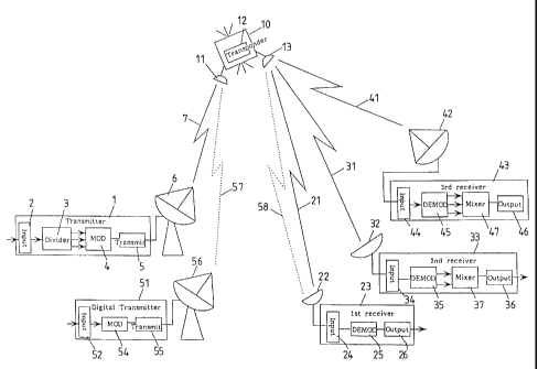
Fig. 1 shows the entire arrangement of a signal
transmission system according to the present invention. A
transmitter 1 comprises an input unit 2, a divider circuit 3,
a modulator 4, and a transmitter unit 5. In action, each
input multiplex signal is divided by the divider circuit 3
into three groups, a first data stream D1, a second data
strecim D2, a third data stream D3, Which are then modulated
by the modulator 4 before transmitted from the transmitter
unit 5. The modulated signal is sent up from an antennal 6
through sr. uplink 7 to a satellite 10 where f' is intercepted
by an uplink antenna 11 and amplified by a transponder 12
before transmitted from a downlink antenna 13 towards the
ground.
The transmission signal is then sent down through three
downlinks 21, 32; and 41 to a first 23, a second 33, and a
CA 02332405 2001-02-06
.... ..._. . ._,. "f:~;~ _~:a~' ... .... :. _. _W
third re~eivor 43 respectively. In the first receiver 23, the
signal intercepted by an antelma 7.2 is fed through an input
unit 24 to a demodulator 25 where its first data stream only
is demodulated, while the second and third data streams are
not recovered, before transmitted further from an outpu: unit
26.
Similarly, the second receiver 33 allows the first and
second data streams of the signal intercepted by an antenna
32 and fed from an input unit 34 to be demodulated by a
demodulator 35 and then, summed by a summer 37 to a single
data stream which is then transmitted further from an output
unit 36.
The third receiver 43 allows all the first, second, and
third data streams of the signal intercepted by an antenna 42
and fed from an input unit 44 to be demodulated by a
demodulator 45 and then, summed by a summer 47 to a single
data stream which is then transmitted further from an output
unit 46.
As understood, the three discrete receivers 23, 33, and
43 have their respective demodulators of different
characteristics such that their outputs demodulated froto the
same frequency band signal of the transmitter 1 contain data
of different sizes. More particularly, three different but
compatible data can simultaneously be carried on a given
frequency band signal to their respective receivers. For
example, each of three, existing NTSC, HDTV, and super )ATV,
digital signals is divided into a low, s high, and a super
21
CA 02332405 2001-02-06
.,.. ..l_. . ..., ~~-» C a-c~ . .. .... . _. ._.
high frequency band components which represent the first, the
second, and the third data stream respectively. Accordingly,
the three different TV signals can be transmitted on a one-
channel frequency band carrier for simultaneous rep~oduction
of a medium, a high, and a super high resolution TV image
respectively.
In service, the NTSC TV signal is intercepted by a
receiver accompanied with a small antenna for demodulation of
a sma:i-sized data, the HDTV signal is intercepted by a
receiver accompanied with a medium antenna for demodulation
of medium-sized data, and the super HDTV signal is
intQrcepted by a receiver accompanied with a large antenna
for demodulation of large-sized data. Also, as illustrated
in Fig. 1, a digital ~ITSC TV signal containing only the first
data stream for digital NTSC TV broaucasting service is fed
to a digital transmitter 51 where it i~ received by an input
unit 52 and modulated by a demodulator 54 before transmitted
further from a transmitter unit 55. The demodulated signal is
then sent up from an antannal 56 through an uplir:k 57 to the
satellite 10 which in turn transmits the same through a
downlink 58 to the first receiver 23 on the ground.
The first receiver 23 demodulates with its demodulator
the modulated digital signal supplied from the digital
transmitter 51 to the original first data stream signal.
25 Similarly, the same modulated digital signal can be
intercepted and demodulated by the second 33 or third
receiver 42 to the first data stream or N'rSC TV signal. In
22
CA 02332405 2001-02-06
....- _'_._ . ~ " '1:~~ .: o'-- . . ..-. :. __
summary, the three discrete receivers 23, 33, and 43 ali can
intercept and process a digital signal of the existing TZ'
system for reproduction.
The arrangement of the signal transmission. system will
be described in more detail.
Fig. 2 is a blocl~ diagram of the transmitter 1, in which
an input signal is fed across the input unit 2 and divided by
the divider circuit 3 into three digital signals containing
a first, a second, and a third data stream respectively.
Assuming that the input signal is a video signal, its
lov frequency band component is assigned to the first data
stream, its high frequency band component to the second data
stream, its super-high frequency band component to the third
data stream. The three different frequency band signals are
fed to a modulator input 61 of the modulator 4. Hare, a
signal point modulating/changing circuit 67 modulates or
changes the positions of the signal points according to an
externally given signal. The modulator 4 is arranged for
amplitude modulation on two 90°-out-of-phase carriers
respectively which are then summed to a multiple QAM signal.
More specifically, the signal from the modulator input 61 is
fed to both a first 62 and a szcond AiVI modulator 63. Alsu, a
carrier wave of cos(2nfct) produced by a carrier generator 64
is directly fed to the first 4M modulator 62 and also, to a
a/2 phase shifter 6E Where it is 90° shifted in phase to a
sin(2nfct) form prior to transmitted to the second AM
modulator 63. The two amplitude modulated signals from the
23
CA 02332405 2001-02-06
_:..- _._.. . -;.._. ~-.~_.--c~:'. .....: . __ ._.
first and second A:'i modulators 62, 63 s:e summed by a summer
65 to a transmission signal which is then transferred to the
transmitter unit 5 for output. The procedure is well known
and will no further be explained.
;, The QA~~t signal will now be described in a common 6x8 or
16 state constellation referring to the first quadrant of a
space diagram in Fig. 3. The output signal of the modulator
4 is expressed by a sum vector of two, Acos2nfct and
Bcos2rcfct, vectors 81, 22 which represent the two 90°-out-of-
phase carriers respectively. When the distal point of a sum
vector from the zero point represents a signal point, the 16
QAM signal has 16 signal points determined by a combination
of four horizontal amplitude values a~, a2, a3, a4 and four
vertical amplitude values b1, b2, b3, b4. The first quadrant
in Fig. 3 contains four signal points 83 at Cll, 84 at C12, 85
at CZZ, and 86 at C~.
Cll is a sum vector of a vector 0-al and a vector 0-bl
and thus, expressed as Cll - alcos2nfct-blsin2~fet -
Acos(2nfct+dn/2).
It is now assumes that the distance between 0 and al in
the orthogonal coordinates of Fig. 3 is A1, between al and a~
i s A2, be tween 0 and b1 i s B1, and be tw een b1 and bl i s BZ .
As shown in Fig. 4, the 16 signal points are allocated
in a vector coordinate, in which each point represents a
four-bit pattern thus to allow Lhe transmission of Tour bit
data per period or time slot.
Fig. 5 illustrates a common assignment of two-bit
24
CA 02332405 2001-02-06
..., . ,__. . .~. ~ 'rl.~'_ _.~cV" ~ . ..._ .. __ "..
patterns to the I6 signal points.
When the dista_~ce betweon twa adjacent signal points is
great, it will be identified by the receiver with much ease.
I-T.ence, it ins desired to space the signal points at greater
intervals. If two particular signal points are allocated near
to each other, they are rarely distinguished and error rate
will be increased. Therefore, it is most preferred to have
the signal points spaced at equal intervals as shown in Fig.
5, in which t;he 16 QAM signal is defined by A1=A2~''
The transmitter 1 of the embodiment is arranged to
divide an input digital signal into a first, a second, and a
third data or bit stream. The 16 signal points or groups of
signal points are divided into four groups. Then, 4 two-bit
patterns of the first data stream are assigned to the four
signal point groups respectively, as shown in Fig. 6. More
particularly, when the two-bit pattern of the first data
stream is 11, one of four signal points of the first signal
point group 81 in the first quadrant is selected depending or~
the content of the second data stream for transmission.
Similarly, when O1, one signal point of the second signal
point gro~:p 92 in the second quadrant is selected and
transmitted. When 00, one signal point of the third signal
point group 93 in the trird quadrant is transmitted and whey.
10, one signal point of the fourth signal point group 94 in
the fourth quadrant is transmitted. Alpo, 4 two-bit patterns
in the second data stream of the 16 QA.M signal, or e.g. 16
four-bit patterns in the second data stream of a 64-state QAM
CA 02332405 2001-02-06
...._ .'_.. :=_ - '~.,~'_ G~~~-.'- ~~~. ..z,. .. _ ...
signal, are assigned to four signal points or sub signal
point groups o~ each of the four signal point groups 91, 92,
93, 94 respectively, as shown in Fig. 7. It should be
understood that the assignment is symmetrical between any two
quadrants. The assignment of the signal points to the four
groups 91, 92, 93, 94 is determined by priority to the two-
bit data of the first data stream. As tile result, two-bit
data of the first data stream and two-bit data of the second
dais stream can be tr anamitted independently. Also, the first
data stream will be demodulated with the use of a common 4
PSK receiver having a given antenna sensitivity. If the
antenna sensitivity is higher, a modified type of the 16 QAM
receiver of the present invention will intercept and
demodulate both t:~a first and second data stream with equal
I5 success.
Fig. 8 shows an ezample of the assignment of the first
and second data streams in two--bit patterns.
When the low frequency band ccmponent of an HDTV video
signal is assigned to the first data stream and the high
frequency component to the second data stream, the 4 PSK
receiver can produce an NTSC-level pictur°_ from the first
data stream and the 16- or 64-state QAM receiver can produce
an !HDTV picture from a composite reproduction signal of the
first and second data streams.
Since tile signal points are allocated at equal
intervals, there is developed in the 4 PSK receiver a
threshold distance between the coordinate axes and the spaded
26
CA 02332405 2001-02-06
. : . . _ . - _ . - . ;. _ ~ ~v ~ '_ _.~. o-~ - . . . . z , - _ . . . .
area of the first quadrant, as shown in Fig. 9. Tf the
threshold distance is ~, a FSh signal having an amplitude
of A,~ will successfully be intercepted. However, the
amplituda has to be ir_creased to a three times greater value
or 3A.1,0 for transmission of a 16 QAM signal while the
threshold distance A~ being mnintained. More particularly,
the energy for transmitting the 16 Q,4M signal is needed nine
times greater than Thai for sending the 4 PSK signal. Also,
when the 4 PSK signal is transmitted in a 16 9Ari mode, energy
waste will be high and reproduction of a carrier signal will
be troublesome. AboL~e all, the energy available for satellite
transmitting is not abundant but strictly limited to minimum
use. Hence, no large-energy-consuming signal transmitting
system will be put into practice until more energy for
satellite transmission is available. It is expected that a
great number of the 4 PSK receivers are introduced into the
market as digital TV broadcasting is soon in service. After
introduction to the market, the 4 PSK receivers will hardly
be shifted to higher sensitivity models because a signal
intercepting characteristic gap between the two, old and new,
models is high. Therefore, the transmission of the 4 PSK
signals MusD not be abandoned.
In this ~espect, a new system is desperately needed for
transmitting the signal point data of a quasi 4 PSK signal in
the 18 WAM mode wi'h the use of less energy. Otherwise, the
limited energy at a satellite station will degrade the entire
transmission system.
27
CA 02332405 2001-02-06
. . . . . _ . _ . ~._ ':a-= - _
The present invention resides in a multiple signal level
arrangement in which the four signal point groups 91, 92, 93
94 are allocated at a greater distance from each other, as
shown in Fig. 10, for minimizing the energy consumption
required for 16 WAM modulation of quasi 4 PSg signals.
For clearing Lhe relation between the signal receiving
sensitivity and the transmitting energy, the arrangement of
the digital transmitter 51 and the first receiver 23 will be
described in more detail referring to Fig. 1.
Both the digital transmitter 51 and the first receiver 23 are
formed of known types far data transmission or video signal
transmission e.g. in TV broadcasting service. As shown in
Fig. 17, the digital transmitter 51 is a 4 P5H transmitter
equivalent to the multiple-bit QAM transmitter 1, shown in
Fig. 2, without AIrI modulation capabllity~. In operation, an
input signal is fed through an input unit 52 to a modulator
54 where it is divided by a modulator input 12i to two
components. The two components are then transferred to a
first two-phase modulator circuit 122 for phase modulation of
a base carrier and a second two-phase modulator circuit 123
for phase modulation of a carrier which is 9d° out of phase
with the base carrier respectiva'.y. Ttvo outputs of the first
arid secorid two-phase modulator circuits 122, 123 are then
summed by' a summer 65 to a composite modulated signal which
is further transmitted from a transmitter unit 55.
'the resultant modulated signal is shown in the space
diagram ~f Fig. 18,
28
CA 02332405 2001-02-06
. ...- . ;_.. . ~;~.. r-.~'_ cW:;w_ . .. ..-. ...
It is l~nown that the four signal points are allocated at
equal distances for achievir_g optimum energy utilization.
Fig. 18 illustrates an example where the four signal points
125, 12fi, 127, 128 rep~esent 4 two-bit patterns, I1, O1, 00,
and 10 respectively. It is also desired for successful data
transfer from the digital transmitter 51 to the first
receiver 23 than the 4 PSh signal from the digital
transmitter 51 has an amplitude of act less than a given
level. More specifically, when the minimum amplitude of the
4 PSK signal needed for transmission from the digital
transmitter 51 to the first receiver 23 of 4 PSK mode, or the
distance between 0 and al in Fig. 18 is A~, the first
receiver 23 successfully intercept any 4 PSK signal having an
amplitude of more than A,~.
The first receiver 23 ie arranged to receive at its
small-diameter antenna 22 a desired or 4 PSg signal which is
transmitted from the transmitter 1 or digital transmitter 51
respectively through the transponder 12 of the satellite 10
acrd demodulate it with the demodulator 24. In more
particular, the first receiver 23 is substantially designed
for interception of a digital TV or data communications
signal of 4 P5K or 2 PSK mode.
Fig. 19 is a block diagram of the first receiver 23 in
which an input signal received by the antenna 22 from the
satellite 12 is fed through the input unit 24 to a carrier
reproducing circuit 131 where a carrier wave is demodulated
and to a x/2 phase shifter 132 where a 90' phase carrier wave
29
CA 02332405 2001-02-06
. ., . . . ~I _ . - . Fu _~ ~.~~_ C~ .a F~' . . . . T . . . . . . .
is demodulated. Also, two 90°-aut-of-phase components of the
input signal are detected by a first 133 and a second phase
detector circuit I34 respectively and transferred tG a first
136 and a secoad discrimination/demcdulation circuit 137
respectively. Two demodulated components from their
respective dlscrimination/demodulation circuits I36 and 137,
which have separately been discriminated at units of time
slot by means of timing signals from a timing wave extracting
circuit 135, are fed to a first data stream reproducing unit
232 where they are summed to a first data stream signal which
is then delivered as an output from the output unit 26.
The input signal to the first receiver 23 will now be
explained in more detail referring to the vector diagram of
Fig. 20. The d PSK signal received by the first receiver 23
from the digital transmitter 31 is expressed in an ideal form
without transmission distortion and noise, usinE four signal
points 151, I52, 153, I54 shown in Fig. 20.
In practice, the real four signal points appear in
particular extended areas shout the ideal signal positions
151, 152, 153, 154 respectively due to noise, amplitude
distortion, and phase error developed during transmission. If
one signal point is unfavorably displaced from its original
pOSitiOn, it will hardly be distinguished from its neighbor
signal point and the error rate will thus be increased. As
the error rate increases to a critical level, the
reproduction of datts becomes less accurate. F'or enabling the
data reproduction at a maximum acceptable level of the error
CA 02332405 2001-02-06
..._- .;_._ . ~;~_,. r-,~._ -'-:o--:- ... ..-.. . ._ ._.
rate, the distance between any two signal points should be
far enough to be distinguished from each other. If Lhe
distance is lA~, the signal point 15I of a 4 PSK signal at
close to a critical error level has to stay in a first
discriminating area 155 denoted by the hatching of Fig. 20
and determined by ~0-a~'?A~ and ~G-b~~?A~. This allows the
signal transmission system to reproduce carrier waves and
thus, demodulate a wanted signal. When the minimum radius of
the antenna 22 is set to r~, the transmission signal of more
than a given level can be intercepted by any receiver of the
system. The amplitude of a 4 PSK signal of the digital
transmitter 51 shown in Fig. 18 is minimum at A.~ and thus,
the minimum amplitude A~ of a 4 PSK signal to be received by
the first receiver 23 is determined equal to A,~. As the
result, the first receiver 23 can intercept and demod~,~late
the 4 PSK signal from the digital transmitter 51 at the
maximum acceptable level of the error rate when the radius of
the antenna 22 is more than r~. If tha transmission signal is
of modified 16- or 64-state QA.~i mode, the first' receiver 23
may find difficult to reproduce its carrier wave. F'or
compensation, the signal points are increased to eight which
are allocated at angles of (n/4+nn/2) ae shown in Fig. 25(a)
and its carrier wave will be reproduced by a 16x
multiplication technique. Also, i' the signal points are
assigned to 16 locations at angles of nn/6 as shown in F'ig.
25(b), the carries of a quasi 4 PSK mode 16 9AM modulated
signal can be reproduced with the carrier reproducing circuit
31
CA 02332405 2001-02-06
._-._ .;_.. . ~'.._- '':'_'_ -:-'-nW.". ... ..-. .. .. ...
131 which is modified for performing 16x frequency
multiplication. At the rime, the signal points in the
transmitter 1 should be arranged to satisfy
A1/(A1+AZ)=tan(n/8) .
Here, a case of receiving a QPSK signal will be
considered. Similarly to the manner performed by the signal
point modulating/changing circuit 67 in the transmitter shown
in Fig. 2, it is also possible to modulate the positions of
the signal points of the QPSg signal shown in Fig. 18
(amplitude-modulation, pulse-modulation, or the like). In
this case, the signal point demcdulating unit I38 ir_ the
first receiver 23 demodulateB the position modulated or
position changed signal. The demodulated signal is outputted
together with the first data stream.
The 16 PSB signal of the transmitter 1 will now be
explained referring to the vector diagram of Fig. 9. When
the horizontal vector distance A1 of the signal point 83 is
greater than A,~ of the minimum amplitude oz the 4 PSK signal
of the digital transmitter 51, the four signal points 83, 84,
85, 86 in the first quadrant of Fig. 9 stay in the shaded or
first 4 PSg signal receivable area 87. When received by the
first receiver 23, the four points of the signal appear in
the first discriminating area of the vector field shown in
Fig. 20. Hence, any of the signal points 83, 84, 85, 86 of
Fig. 9 can be translated into the signal level 151 of Fig. 20
by the first receiver 23 so that the two-hit pattern of 11 is
assigned to a corresponding time slot. The two-bit pattern
32
CA 02332405 2001-02-06
of 11 is identical to 11 of the first signal point group 91
or first data stream of a signal from the transmitter 1.
Equally, the first data stream will be reproduced at the
second, third, or fourth quadrant. As t'~e result, the first
receiver 23 reproduces two-bit data of the first data stream
out of the plurality of data streams in a 16-, 32-, or 64-
state QA.M signal transmitted from the transmitter 1~ The
second and third data streams are contained in four segments
of the signal point group 91 and thus, will not affect on the
demodulation of the first data stream. They may however
affect the reproduction of a carrier wave and an adjustment,
described later, will be needed.
If the transponder of a satellite supplies an abundance
of energy-, the forgoing technique of 16 to 64-state WAM mode
transmission will be feasible. However, the transponder of
the satellite in any existing satellite transmission system
is strictly limited in the power supply due to its compact
size and the capability of solar batteries. If the
transponder or satellite is increased in size thus weight,
its launching cost will soar. This disadvantage will rarely
be eliminated by traditional techniques unless the cost of
launching a satellite rocket is raduced to a considerable
level. In the existing system, a common communications
satellite provides as low as 20 W of power supply and a
common broadcast satellite offers 100 W to 200 W at best. For
transmission of such a 4 PSK signal in the symmetrical 16-
state QAr1 mode as shown in Fig. 9, the minimum signal paint
33
CA 02332405 2001-02-06
._.- .._._ _ -_.. 't.,~_ ~~~-:'~ ... ..-
distance is needed 3A.~ as the I6 C~A:~1 amplitude is ezpressed
by 2A1=,~. Thus, the energy needed for the purpose is nine
times greater than that for transmission of a common 4 PSK
signal, in order to maintain compatibility. Also, any
conventional satellite transponder can hardly provide a power
for enabling such a small antenna of the 4 PSK first receiver
to intercept s transmitted signal therefrom. For example, in
the existing 40W system, 360' is needed for appropriate
signal transmission and will be unrealistic in the respect of
cost.
It would be under stood that the symmetrical signal
state QAhi technique is most effective when the receivers
equipped with the same sized antennas are employed
corresponding to a given transmitting power. Another novel
technique will however be preferred for use with the
receivers equipped with different sized antennae.
In more detail, while the 4 PSK signal can be
intercepted by a common low coat receiver system having a
small antenna, the 16 pA.M signal is intended to be received
by a high cast, high quality, multiple-bit modulating
receiver system with a medium or large sized antenna which is
designed for providing highly valuable services, e.g. HDTV
entertaiiiments, to a particular person who invests more
money. This allows both 4 PSK and 16 QAM signals, if desired,
with a 64 DMA, to be transmitted simultaneously with the help
of a small increase in the transmitting power.
For example, the transmitting power can be maintained
34
CA 02332405 2001-02-06
. : : .- ... _ . . . ~: . . ' '~~,~'_ c.~.e'; ' .' .. . . - . . . . . . .
low when the signal points are allocated at Al= AZ as shown
in Fig. 10. The amplitude A(4) for transmission of 4 PSK data
is expressed by a vector 96 equivalent to a square root of
(A1+AZ)Z+(B1+B2)2. Then,
' A ( 4 ) ~ ~A1Z+B1ZA~2+~~ 2A~2
~ A ( 16 ) ~ ~-. ( Al+A') Z+ ( B1+BZ ) ~ 4A,~2* 4A,~~=s~2
iA(16)~/~A(4)1-2
Accordingly, the 16 AAM signal can be transmitted at a
two times greater amplitude and a four times greater
transmitting energy than those needed for the 4 PSK signal.
A modified 16 QAM signal according to the present invention
will not be demodulated by a common receiver designed for
symmetrical, equally distanced signal point QAM. However, it
can be demodulated with the second receiver 33 when two
threshold A1 and AZ are predetermined to appropriate values.
At Fig. 10, the minimum distance between two signal points in
the first segment of the signal point group 91 is A1 and
AZ/2A1 is established as compared with the distance 2A1 of 4
PSH. Then, as A,=A," the distance becomes 1/2. This explains
that the signal receiving sensiti~~ity has to be two times
greater for the same error rate and four times greater for
the same signal level. For having a four times greater value
of sensitivity, the radius r2 of the antenna 32 of the second
receiver 33 has to be two times greater than the radius r1 of
the antenna 22 of the first receiver 23 thus satisfying
r~2rl. For example, the antenna 32 of the second receiver 33
is 60 cm diameter when the antenna 22 if the first receiver
CA 02332405 2001-02-06
. . _ . . _ . . . ~ .. -' ._ _ :-.. _
- - ._, ~ .~,_ _. .. . . ~z~
23 is 30 cm. In this manr_er> the second data stream
representing the high frequency component of an HDTV will be
carried on a signal channel and demodulated successfully. As
the second receiver 33 intercepts the second data stream or
a higher data signal, its owner can enjoy a return of high
investment. Hence, the second receiver 33 of a high price may
be accepted. Ac the minimum energy far transmission of 4 PSH
data is predetermined, the ratio n,fi of modified 18 APSK
1
transmitting energy to 4 PSK transmitting energy will be
1U calculated tv the antenna radius r2 of the second receiver 33
using a ratio between A1 and A2 shown in ~'ig. 10.
in particular, nlfi is expressed by ( (A1+AZ)/Al)Z which is
the minimum energy for transmission of 4 PSK data. As the
signal point distance suited for modified 16 6~AM interception
is AZ, the signal point distance for 4 PST interception is
2A1, and the signal point distance ratio is AZ/2A1, the
antenna radius rZ is determined as shown in Fig. 11, in which
the curve 101 represents the relation between the
transmitting energy ratio nls and the radius r2 of the antenna
22 of the second receiver 23.
Also, the point 102 indicates transmission of common 16
QAM at the equal diatance signal state mode where the
transmitting energy is nine times greater and thus will no
more be practical. As apparent from the graph of Fig. 11, the
antenna radius rZ of the second receiver 23 cannot be reduced
further even if n16 is inc~eased more than 5 times.
The transmitting energy at the satellite is limited to
36
CA 02332405 2001-02-06
..._- _~._.- . ~'.__, !~.~~ ='-;o-c' ... ... _. .. ...
a small value and thus, nls preferably stays not more than 5
times the value, as denoted by the hatching of Fig. 11. The
point 104 within the hatching area 103 indicates, for
example, that the antenna radius r2 of a two times greater
value is matched with a 4x value of the transmitting energy.
Also, the point 105 represents that the transmission energy
should be doubled when rZ is about 5x greater. Those values
are all within a feasible range.
The value of nls not greater than 5x value is eapresced
us ing A1 and AZ as
nls = ((AlfA2)/Al)Z~ 5
Hence, AZ<_1.23A1.
If the distance between any two signal paint group
segments shown in Fig. 10 is 2A(4) and the maximum amplitude
is 2A(16), A(4) and A(16)-A(4) are proportional to A1 and AZ
respectively. Hence, (A(16))~5(A(14))Z ie established.
The action of a modified 64 ASPK transmission will be
described as the third receiver 43 can perform 64-state QAM
demodulation.
Fig. 12 is a vector diagram in which each signal point
group segment contains 16 signal points as compared with 4
signal. points of Fig. 10. The first signal point group
segment 91 in Fig. 12 has a 4x4 matrix of 16 signal points
allocated at equal interval6 including the point 170. Fer
providii:g compatibility with 4 PSK, A1?A~ has to be
satisfied. If the radius of the antenna 42 of the third
receiver 43 is r3 and the transmitting energy is n~, the
37
CA 02332405 2001-02-06
. . : :- . ; _ . . . ' '. .' ';:.~'_ ='J''FT .~ .. . . - ~ . . . . . . ,
equation 18 e7Cpre99ed 8&:
r~2 = ~6d/~n-1)'1r:2
This relation between r3 and n of a 64 QAr'"i signal is
also shown in the graphic representation of Fig. 13.
It is under stood that the signal point assignment shown
in Fig. 12 allows the second receiver 33 to demodulate only
two-bit patterns of 4 PSK data. Hence, it is desired for
having compatibility between the first, second, and third
receivers that the second receiver 33 is arranged capable of
demodulating a modified 16 QAM form from the 64 WAM modulated
signal.
The compatibility between the three discrete receivers
can be implemented by three-level grouping of signal points,
as illustrated in Fig. 14. The description will be made
referring to the first quadrant in which the first signal
point group segment 91 represents the two-bit pattern 11 of
the first data stream.
In particular, a first sub segment 181 in the first
signal point group segment 91 is assigned the two-bit pattern
11 of the second data stream. Equally, a second 182, a third
183, and a fourth sub segment 184 are assigned O1, 00, and 10
of the same respectively. This assignment is identical to
that shown in Fig. 7.
The signal point allocation of the third data stream
will now be explained referring to the vector diagram of Fig.
15 which shows the first quadrant. As shown, the four signal
points 201, 205, 209, 213 represent the two-bit pattern of
38
CA 02332405 2001-02-06
11, the signal points 202, 206, 210, 214 represent O1, the
signal points 203, 207, 211, 215 represent 00, and signal
points 204, 208, 212, 216 represent 10. Accordingly, the
two-bit patterns of the third data stream can be transmitted
separately of the first and second data streams. In other
words, two-bit data of the three different signal levels can
be transmitted respectively.
As understood, the present invention permits not only
transmission of six-bit data but also interception of three,
two-bit, four-bit, and six-bit, different bit length data
with their respective receivers while the signal
compatibility remains between three levels.
The signal point allocation for providing compatibility
between the three levels will be described.
As shown in Fig. 15, Al?A,~ is essential for allowing the
first receiver 23 to receive the first data stream.
It is needed to space any two signal points from each
other by such a distance that the sub segment signal points,
e.g. 182, 183, 184, of the second dnta stream shown in Fig.
15 can be distinguished from the signal point 91 saown in
Fig. 10.
Fig. 15 shows that they are spaced by 2/3A2. In this
case, the distance between the two signal points 201 and 202
in the first sub segment 181 is AZ/6. Tre transmitting energy
needed for signal interception with the third receiver 43 is
now calculated. If the radius of the antenna 32 is r~ and the
needed transmitting energy is n~ Limes the 4 PSK transmitting
39
CA 02332405 2001-02-06
~ -
..._ . ._:- . .t. u:,~1_ C'r'-'E= .... ..:: -. ...
energy, the equation is expressed as:
r3Z= ( 12r1)2/ (n-1 )
This relation is also denoted by the curve 2I1 in Fig. 16.
For example, if the transmitting energy is 6 0° 9 times
greater than that for 4 PSK transmission at the point 223 or
222, the antenna 32 having a radius of 8x or 6x value
respectively can intercept the first, second, and third data
streams for demodulation. As the Fignal point distance of the
second data stream is close to 2/3A2, the relation between r1
and r2 is expressed by:
r2~=(3r1)~/(n-1)
Therefore, the antenna 32 of the second receiver 33 has to be
8 little bit increased in radius as denoted by the curve 223.
As understood, whsle the first and second data streams
are transmitted trough a traditional satellite which provides
a small signal transmitting energy, the third data stream can
also be transmitted through a future satellite which provides
a greater signal transmitting energy xithout interrupting the
action of the first and second receivers 23, 33 or with no
need of modification of the same and thus, both the
compatibility and the advancement Hill highly be ensured.
The signal receiving action of the second receiver 33
will first be described. As compared with the first receiver
23 arranged for interception with a small radius r1 antenna
and demodulatiar. of the 4 PSK modulated signal of the digital
transmitter 51 or the first data stream of the signal of the
transmitter 1, the second receiver 33 is adopted for
CA 02332405 2001-02-06
....- . ,_._ . ~..- ~_ _ .-,~-__ .:. -
perfectly demodulating the lti signal state two-bit data,
shown in Fig. 10, or se;:ond data stream of the 1B QAM signal
from the transmitter 1. In total, fou~-bit data including
also the first data stream can be demodulated. The ratio
between Ai and AZ is however different in the two
transmitters. The two different data are loaded to a
demodulation controller 23I of the second receiver 33, shown
in Fig. 21, which in turn supplies their respective threshold
values to the demodulating circuit for AM demodulation.
The block diagram of the second receiver 33 in Fig. 21
is simila: in basic conBtructivn to that of the first
receiver 23 shown in Fig. 18. The difference is that the
radius r2 of the antenna 32 is greater than ry of the antenna
22. This allows the second receiver 33 to identify a signal
component involving a smaller signal po_nt distance. The
demodulator 35 of the second receiver 33 also contains a
first 232 and a second data stream reproducing unit 233 in
addition to the demodulation controller 231. There is
provided a first discrimination/reproduction circuit 136 for
2U AM demodulation of modified 16 Qr..'~ signals. As understood,
each carrier is a four-bit signal having two, positive and
negative, threshold values about the zero level. As apparent
from the vector diagram, of Fig. 22, the threshold values are
varied depending on the transmitting energy of a transmitter
since the transmitting signal of the embodiment is a modified
16 QAM signal. When the reference threshold is TH16, it is
determined by, as shown in Fig. 22:
41
CA 02332405 2001-02-06
. . : _ . . _ . _ . '. . - -_ - ~-~ .~3- , . - . ,
THIo = f Al+A~/ 2 ) / t Ai+AZ
the various data for demodulation including A1 and A2 or
'L'H=5, and the value m for multiple-bit modulation are also
transmitted from the transmitter 1 as carried in the first
data stream. The demodulation controller 231 may be arranged
for recovering such demodulation data through statistic
process of the received signal.
A way of determining the shift factor A1/AZ will
described with reference to Fig. 26. A change of the shift
factor A~/AZ causes a change of the threshold value. Increase
of a difference of a value of AljA2 set at the receiver side
from a value of A~/AZ set at the transmitter side will
incresse the error rate. Referring to Fig. 20, the
demodulated signal from the second data stream reproducing
1~ unit 233 nay be fed back to the demodulation controller 231
to change the shift factor A1/A2 in a direction to increase
the error rate. By this arrangement, the third receiver 43
may not demodulate the shift factor A1/AZ, so that the circsit
construction can be simplified. Further, the transmitter may
not transmit the shift factor A1/A2, so that the transmission
capacity can be increased. This technique can be applied also
to the second receiver 33.
'The demodulation controller ~'31 has a memory 231a for
storing therein different threshold values (i.e., the shift
factors, tl.e number of signal points, the synchronisation
rules, etc.) which correspond to different channels of TV
broadcast. When receiving one of the channels again, the
42
CA 02332405 2001-02-06
. ., . . . _ . _ . . . _ - .~ ~ ~.T'-e-'- . .. . . . . . . . . .
values corresponding to the receiving channel will be read
out of the memory to thereby stabilize the reception quickly.
If the demodulation data is lost, the demodulation of
the second data stream will hardly he execsted. This will be
explained referring to a flow chart shown in Fig. 24.
Even if the demodulation data is not available,
demodulation of the 4 PSfi at Step 313 and of the first data
stream at Step 301 can be implemented. At Step 302, the
demodulation data retrieved by the first data stream
reproducing unit 232 is transferred to the demodulation
controller Z31. If m is 4 or 2 at SteF 303, the demodulation
controller 231 triggers demodulation of 4 PSg or 2 PSg at
Step 313. lf~ not, the procedure moves to Step 310. At Step
305, two threshold values TH8 and THIS are calculated. The
threshold value TH16 for A_~S demodulation is fed at Step 306
from the demodulation controller 231 to both the first 136
and the second discrimination/reproduction circuit 137.
Hence, demodulation of ~he modified 16 QAM signal and
reproduction of the Second data stream can be carried out at
Steps 307 and 315 respectively. At Step 308, the error rate
is examined and if high, the procedure returns to Step 313
for repeating the 4 PSIC demedulati;:n.
As shown in Fig. 22, the signal points 85, 83, are
aligned on a line at an angle of cos(c~t+Ln/2) while 84 and 86
are ozf the line. Hence, the feedback of a second data
stream transmitting carrier wave data from the second data
stream reproducing unit 233 to a carrier reproducing circuit
43
CA 02332405 2001-02-06
....- .._._ ~_._. ~-~_ W.:-_- .--. -. -..
131 is carried out so that no carrier needs to be extracted
at the timing of the signal points 84 and 96.
The transmitter 1 is arranged to transmit carrier timing
signals at intervals of a given time with the first data
stream for the purpose of compensation for no demodulation of
the second data stream. The carrier timing Signal enables to
identify the signal points 83 and 85 of the first data stream
regardless of demodulation of the second data stream. Hence,
the reproduction of carrier wave can be triggered by the
transmitting carrier data to the carrier reproducing circuit
131.
It is then examined at Step 304 of the flow chart, of
Fig. 24 whether m is 16 or not upon receipt of such a
modified 64 QA,M signal as shown in Fig. 23. At Step 310, it
is also examined whether m is more than 64 or not. If it is
determined at Step 311 that the received signal has no equal
distance signal point constellation, the procedure goes to
Step 312. The signal point distance THE of the modified 64
QAM signal is calculated from:
THE _ (A1+AZ/2)/(A1+AZ)
This calculation is equivalent to that of THl6 but its
resultant distance between signal points is smaller.
If the signal point distance in the first sub segment
181 is A3, the distance between the first 181 and the second
sub segment 182 is expressed by (AZ 2A~). Then, the average
distance is (AZ-2A3)/(Al+AZ) which is designated as due. When
d~ is smaller than TZ which represents the signal point
44
CA 02332405 2001-02-06
. . . .- . ~ _ .. . ... _. . .~ _ =.-._o___ ,. . . : . -
discrimination capability of the second receiver 33, any two
signal points ir. the segment will hardly be distinguished
from each other. This judgement is executed at Step 313. If
d~ is out of a permissive range, the procedure moves back to
Step 313 for 4 PSK mode demodulation. If d~ is with~'_n the
range, the procedure advances to Step 335 for allowing the
demodulation of 16 QAM at Step 307. If it is determined at
Step 308 that tine error rate is too high, the procedure goes
back to Step 313 for 4 FSK mode demo3ulation.
When the transmitter 1 supplied a modified 8 QAM signal
such as shown in Fig. 25(x) in which all the signal points
are at angles of cos(2~f+n~u/4), the carrier waves of the
signal are lengthened to the same prase and will thus be
reproduced with much ease. At the time, two-bit data of the
I5 first data stream are demodulated with the 4-PSK receiver
while one-bit data of the second data stream is demodulated
with the second receiver 33 and the total of three-bit data
can be reproduced.
The third receiver 43 will be described i.n more detail.
Fig. 26 shows a block diagram of the third receiver 43
simi tar to that of tl:e second rcce? ver 33 in Fig . 21 . The
difference is that a third data stream reproducing ur:it 234
is added and also, the discrimination;reproduction circuit
has a capability of identifying eight-bit data. The anzPnna
42 of the third receiver 43 has a radius r~ greater Lhan rZ
thus allowing smaller distance state signals, e.g. 32- or 64-
state QAM signals, to be demodulated. For demodulation of the
CA 02332405 2001-02-06
. . . _ . _ . . - . . :. ; _ _,-..~_-_ . _ - .
fi4 QAM signal, the first discrimination/reproduction circuit
13~ has to identify 8 digital levels of the detected signal
in Which seven different threshold levels are involved. As
one of the threshold values is zero, three are contained in
the first quadrant.
Fig. 27 shows a space diagram of the signal in which the
first quadrant contains three different threshold values.
As shown in Fig. 27, when the three normalized threshold
values are TH1~, TH2~, and TH3~, they are expressed by:
TH1~ _ (A1+A3/ 2 ) / (Al+Ay )
TH2~ _ (Al+AZ/2)/(Al+AZ) and
TH3~ _ (A1+AZ-A3/2 ) / (A1+AZ)
Through AM demodulation of a phase detected signal using
the three threshold values, the third data stream can be
reproduced like the first and second data stream explained
with Fig. 21. The third data stream contains e.g. four
signal points 201, 202, 203, 204 at the first sub segment 181
shown in Fig. 29 which represent 4 values of two-bit pattern.
Hence, eiz digits or modified 64 QAM signals can be
demodulated.
The demodulation controller 231 detects the value m, Al,
AZ, and Az from the demodulation data contained in the first
data stream demodulated at the first data stream reproducing
unit 232 ar.d cnlculates the three threshold values TH1~,
TH2~, amd TH3~ which are then fed to the first 136 and the
second dis~rimination/reproduction circuit 137 so that the
modified 64 QAM signal is demodulated with certaint;r. Also,
46
CA 02332405 2001-02-06
....L .1~. . F . ~~%,::_ ..J.nr~ .... .. ...
if the demodulation data have been scrambled, the modified 64
QAI~i signal can be demodulated only with a specific or
subscriber rsceiver. Fig. 28 is a flow chart showing the
action of the demodulation controller 23i for modified 6Q GRAM
signals. The difference from the flow chart for demodulation
of 16 QA."~ shown in Fig. 24 will be explained. The procedure
moves from Step 304 to Step 320 where it is examined whether
m=32 or not. If m=32, demodulation of 32 GL~ signals is
ezecuted at Step 322. If not, the procedure moves to Step 321
IO where it is examined Whether m=84 ur not. If yes, A3 is
examined at Step 323. If A3 is smsller than a predetermined
value, the procedure moves to Step 3C~S ar_d the same sequence
as of ~'ig. 24 is implemented. If It is judged at Step 323
that A3 is not smaller than the predetermined value, the
procedure goes to Step 324 where the threshold values are
calculated. At Step 325, the calculated threshold values are
fed to the first and second discrimination/reproduction
circuits and at Step 326, the demodulation of the modified 64
QAM signal is carried out. Then, the first, second, and third
data streams are reproduced at Step 32?. At Step 328, the
error rate is examined. If the error rate is high, the
prGc:edure moves to Step 305 where the 16 G1.~1 demodulation is
repeated and if low, the demodulation of the 64 Q~1M is
continued.
The action of carrier wave reproduction needed for
ezecution of a satisfactory demodGlating procedure will now
be described. The scope ef the present invention includes
4~
CA 02332405 2001-02-06
- . ; _ . - . ~; . - i-.~ _ .:-:~-__ . . -: . - . . . .
reproduction of the first data stream of a modified 16 or 64
QpM signal with the use of a k PST receiver. However, a
common 4 PSg receiver rarely reconstructs carrier waves, thus
failing to perform a correct demodulation. For compensation,
some arrangements are necessary at oozh the transmitter and
recQiver sides.
Two techniques for the compensation are provided
according to the present invention. A first technique relates
to transmission of signal points aligned at angles of (2n-
1)n/4 at intervals of a given time. A second technique offers
transmission of signal points arranged at intervals of an
angle of nn/8.
According to the first technique, the eight signal
points including 83 and 85 are aligned at angles of n/4,
3n/4, 5n/4, and 7n/4, as mown in Fig. 38. In action, at
least one of the eight signal points is transmitted during
sync time slot periods 452, 453, 454, 455 arranged at equal
intervals of a time in a time slot gap 451 shown in the time
chart of Fig. 38. Any desired signal points are transmitted
during the other time slots. The transmitter 1 is also
arranged to assign a data for the time slot interval to the
sync timing data region 499 of a sync data block, as shown in
Fig. 41.
The content of a transmitting signal will be ezplained
in more detail referr_ng to Fig. 41. The time slot group 451
containing the sync time slots 452, 453, 454, 455 represents
a unit data stream or block 491 carrying a data of Dr_.
48
CA 02332405 2001-02-06
....- _'__- '_.:
~", ~ ~ ~ ~ . . . T . . . . . v
The sync time slots in the signal are arranged at equal
intervals of a given time determined by the time slot
interval or sync timing rata. Hence, when the arrangement of
the sync time slots is detected, reproduction Gf carrier
waves will be executed slot by slot through extracting the
sync timing data Prom their respective time slots.
Such a sync timing data S is contained in a sync block 493
accompanied at the front end of a data frame 492, which is
consisted of a number of the sync time slots denoted by the
hatching in Fig. 41. Accordingly, the data to be extracted
for carrier wave reproduction are increased, thus allowing
the 4 PSK receiver to reproduce desired carrier waves at
higher accuracy and efficiency.
The sync block 493 comprises sync data regions 496, 497,
lb 498,---con~aining sync data S1, S2, S3,---respectively- which
include unique words and demodulation data. The phase sync
signal assignment region 499 is accompanied at the end of the
sync block 493, which holds a data of I? including
information about interval arrangement and assignment of the
sync time slots.
The signal point data in the phaBe sync time slot has a
particular phase and can thus be reproduced by the 4 PSK
receiver. Accordingly, IT in the phase sync signs). assignment
region 499 can be retrieved without error thus ensuring the
reproduction of carrier waves at accuracy.
As shown in Fig. 41, the sync black 493 is followed by
a demodulation data block 501 which contains demodulation
49
CA 02332405 2001-02-06
. ' r . . - i-.= '_ _'-~:.-~ ~ . . : . . . . . . . .
data aboLt threshold voliages needed for demodulation of the
modified multiple-bit SAM signal. This data Ls essential for
demodulation of the multiple-bit QAM signal and may
preferably be contained in a region 502 which is a part of
the sync block 493 for ease of retrieval.
Fig. 42 shows the assignment of signal data for
transmission of burst form signals through a TDMA method.
The assignment is distinguished from that of Fig. 41 by
the fact that a guard period 521 is inserted between any two
adjacent Dn data blocks 491, 491 for interruption of the
signal transmission. Also, each data block 491 is
accompanied at front end a sync region 522 thus forming a
data block 492. During the sync region 522, the signal
points at a phase of (2n-1)x/4 are only transmitted.
Accordingly, the carrier Wave reproduction will be feasible
with the 4 PSH receiver. More specifically, the sync signal
an3 carrier waves can be reproduced through the TDMA method.
The carrier wave reproduction of the first receiver 23
shown ir. Fig. 19 will be explained in more detail referring
2C to Figs. 43 and 44. As shown in Fig. 43, an input signal is
fed thrUUgh the input unit 24 t.o a sync detector circuit 5x1
where it ie sync detected. A demodulated signal from the
sync det,e~tor 541 is transferred to an output circuit 542 for
reproduction of the first data stream. A data of the phase
sync signal assignment data region 499 (shown in Fig. 41) is
retrieved with an extracting timing controller circuit 543 so
that the timing of sync signals of f2n-1)n/4 data can be
CA 02332405 2001-02-06
:..- ..-,_.. . ~~._- ~~-,_'.'_ ='-:~o-:." .,.. ..:. .. __ .~.
acknowledged and transierrzd as a phase sync control gulse
561 shown ir. Fig. 44 to a carrier reproduction controlling
circuit 544. Also, the demodulated signal of the sync
detector circuit 541 is fed to a frequency multiplier circuit
5C5 Where it is 4x rauitiplied prior to transmitted to the
carrier reproduction :.ontrolling circuit 544. The resultant
signal denoted by 562 in Fig. 44 contains a true phase data
563 and other data. As illust~at.ed in a time chart 564 of
Fig. 44, the phase sync time slots 452 carrying the {2u-1)><!4
data are also contained at equal intervals. At the carrier
reproducing controlling circuit 544, the signal 562 is
sampled by the phase sync control pulse 561 to produce a
phase sample signal 565 which is then converted through
sample-hold action to a phase signal X66. The phase signal
566 of the carrier reproduction controlling circuit 544 is
fed across a loop filter 546 to a VCO 547 where its relevant
carrier wave is reproduced. The reproduced carrier is then
sent to the sync detector circuit 541.
In this manner, the signal point data of the {2n-1)rc/4
phase denoted by the shaded areas in Fig. 39 is recovered and
utilized Bo that a correct carrier ware can be reproduced by
4x or 16x frequency multiylication. Although a plurality of
phases are reproduced at the time, the absolute phases of the
carrier can be successfully be identified with the used of a
unique word assigned to the sync region 496 shown in Fig. 41.
For transmission of a modif led 64 GlAM signal such as
shown in Fig. 40, signal points in the phase sync areas 471
51
CA 02332405 2001-02-06
._.. .._._ . T::, '~-~_ c"='-'Fr . . ..z. ,. __.
at the (2n-1)n/4 phase denoted by the hatching are assigned
to the sync time slots 452, 452b, etc. Its carrier car be
reproduced hardly with a common 4 PSK receiver but
successfully with the first receiver 23 of 4 PSB mode
provided with the carrier reproducing circuit of the
embodiment.
The foregoing carrier reproducing circuit is of COSTAS
type. A carrier reproducing circuit of reverse modulation
type will now be explained according to the embodiment.
Fig. 45 shows a reverse modulation type carrier
reproducing circuit according to the present invention, in
which a received signal is fed from the input unit 24 to a
sync detector circuit 541 for producing a demodulated signal.
Also, the input signal is delayed by a first delay circuit
591 to a delay signal. The delay aigilal is then transferred
to a quadrature phase modulator circuit 592 where it is
reverse demodulated by the demodulated signal Prom the sync
detector circuit 541 to a carrier signal. The carrier signal
is fed through a carrier reproduction controller circuit 544
to a phase comparator 593. A carrier wave produced by a VCO
547 is delayed by a second delay circuit 594 to a delay
signal which is also fed to the phase comparator 593. At the
phase comparator 594, the reverse demodulated carrier signal
is compared in phase with the delay signal thus producing a
phase difference signal. The phase difference signal sent
through a loop filter 546 to the VCO 547 which in turn
produces a carrier wave arranged in phase with the received
52
CA 02332405 2001-02-06
...-. ,.._. . ~ .. ~ '~-.~: _~.o-::L . . .... . .. ...
carrier wave. In the same manner as of the COS1'AS carrier
reproducing circuit shown in Fig. 43, an extracting timing
controller circuit 543 performs sampling of signal points
contained i.n the hatching areas of Fig. 39. Accordingly, the
carrier wave of a 16 or 64 eA.M signal can be reproduced with
the 4 PSH demodulator of the first receiver 23.
The reproduction of a carrier wave by 16x frequency
multiplication will be explained. The transmitter 1 shown in
Fig. 1. is arrringed to modulate and transmit a modified 16 QAM
signal with assignment of its signal points at nn/8 phase as
shown in Fig. 46. At the first receiver 23 shown in Fig. 19,
the carrier Wave can be reproduced with its COSTAS carrier
reproduction controller circuit containing a 16a multiplier
circuit 661 shown in Fig. 48. The signal points at each ntc/8
phase shown in Fig. 46 are processed at the first quadrant b
the action of the 16x multiplier circuit 661, whereby the
carrier will be reproduced by the combination of a loop
filter 546 and a VCO 541. Also, the absolute phase may be
determined from 16 different phases by assigning a unique
word to the sync region.
The arrangement of the 16x multiplier circuit will be
explained referring to Fig. 48. A sum signal and a difference
signal are produced from the demodulated signal by an adder
circuit 662 and a subtraeter circuit 663 respectively and
then, multiplied each other by a multiplier 664 to a cos 26
signal. Also, a multiplier 665 produces a sin 26 signal. The
two signals are then multiplied by a multiplier 656 tv a sin
53
CA 02332405 2001-02-06
....- . n..- . ~.'-_ ~-.~._ :'-.-~ - .~.. ..7. .. .. ..
4A signal.
Similarly, a sin 88 signal is produced from the two, sin
28 and cos 28, signals by the combination of an adder circuit
667, a subtracter circuit fi68, and a multiplier 670.
Furthermore, a sin 16A signal is produced by the combination
of an adder circuit B71, a subtracter circuit 672, and a
multiplier 673. Then, the 16a multiplication is completed.
Through the foregoing 16z multiplication, the carrier
wave of all the signal points of the codified 1B QA~f signal
shown in Fig. 46 will successfully be reproduced without
extracting particular signal points.
Eowever, reproduction of the carrier wave of the
modified 64 QAM signal shown in Fig. 47 can involve an
increase in the error rate due to dislocation of some signal
1~ points from the sync areas 471.
Two techniQues are known for compensation for the
consequences. One is inhibiting transmission of the signal
points dislocated from the sync areas. This causes the total
amount oP transmitted data to be reduced but allows the
arrangement to be facilitated. The other is providing the
sync t-me slots ae described in Fig. 38. In more particular,
the signal points in the nn/8 sync phase areas, e.g. 471 and
4'1a, are transmitted during the period of the corresponding
sync time slots in ~he time slot group 951. This triggers an
accurate synchronizing action during the period thus
minimizing phase error.
As row understood, the 16x multiplication allows the
~4
CA 02332405 2001-02-06
simple 4 PSk receiver to reproduce the carrier wave of a
modified 16 or o4 vAM signal. Also, the ir_sertion of the
sync time slots causes the phasic accuracy to be increased
during the reproducticn of carrier waves from a modified 64
QAM signal.
As set forth above, the signal transmission system of
the present invention is capable of transmitting a plurality
of data on a single carrier wave simultaneously in the
multiple signal level arrangement.
I0 More specifically, three different level receivers which
have discrete characteristics of signal intercepting
sensitivity and demodulating capability are provided in
relation to one single transmitter so that any one of them
can be selected depending on a wanted data size to be
demodulated which is proportional to the price. When the
first receiver of low resolution quality and low price is
acquired together with a small antenna, its owner can
intercept and reproduce the first data stream of a
transmission Signal. When the second re~aiver of medium
resolution quality and medium price is acquired together with
a medium antenna, its owner can intercept and reproduce both
the first and second data streams of the signal. When the
trird receiver of high resolutio:l qut~lity and high price is
acquired with a large antenna, its owner caa intercept and
reproduce all the first, second, and third data streams of
the signal.
If the first receiver is a home-use digital satellite
CA 02332405 2001-02-06
. . . _- . :_ _ . . ~~-. .. ''-.~'_ c~.y ,'-- .~ .. . . : . . . . _ .
broadcast receiver of low price, it will overwhelmingly be
welcome by a majority of viewers. The second receiver
accompanied with the medium antenna costs more and will be
accepted by not common viewers but particular people who
wants to enjoy HDTV services. The third receiver accompanied
with the large antenna at least before the satellite output
is increased, is not appropriated for home use and will
possibly be used in relevant. industries. For example, the
third data stream carrying super HDTV signals is transmitted
via a satellite to subscriber cinemas which can thus play
video tapes rather than traditional movie films and run
movies business at low cost.
When the present invention is applied to a TV signal
transmission service, tY:ree different quality pictures are
carried on one signal channel wave and will offer
compatibility with each other. Although the first embodiment
refers to a 4 PSK, a modified 8 QAM, a modified 16 QAM, and
a modified 64 QAM signal, other signals will also be employed
with equal success including a 32 QAM, a 256 QAIrt, an 8 PSK,
a 16 PSK, a 32 PSK signal. It would be understood that the
present invention is not limited to a satellite transmission
system and will be applied to a terrestrial communications
system or a cable transmission system.
Embodiment 2
A second embodiment of the present invention is featured
in which the physical multi-level arrangement of the first
embodiment is divided into small levels through e.g.
56
CA 02332405 2001-02-06
. . : :- . _ . - ~-- _,' '~:.:,'_ .~ ,-c' . . : . . . . . . . .
discrimination in error correction capability, thus forming
a logic nult~-18V61 construction. In the first embodiment,
each mLlti-level channel has different _evels in the electric
signs: amplitude or physical demodulating capability. The
second embodiment offers different levels in the logic
reproduction capability such as error correction. For
exempla, the data D1 in a multi-level channel is divided into
two, D~_1 and D1_Z, components and D1_1 is mire increased in the
error correction capability than D~_Z for discrimination.
Accordingly, as the error detection and correction capability
is different between D,,_l and Dl_~ et demodulation, Dl_1 can
successfully be reproduced within a given error rate when the
C/N level of an original transmitting signal is as low as
disenabling the reproduction of D1_2. This will be implemented
using the logic multi-level arrangement.
More specifically, the logic multi-level arrangement is
consisted of dividing data of a modulated nulti-level channel
and discriminating distances between error correction codes
by mixing error correction codes with product codes for
varying error correction capability. Hence, a more multi-
level signal tan be transmitted.
In fact, a D1 channel is divided into two sub cha.r~els
D1_1 and DI_Z and a DZ channel is divided into two sub channels
DZ_1 and D~2.
This kill be explained in more detail referring to Fig.
87 in whi ch D1_1 is reproduced from a lowest C/N signal . If
the C/N rate is d at minimum, three components Dl_~, D2_1 and
J7
CA 02332405 2001-02-06
....- . :_._ . -:-_.. ~.~.._ c~.-~,~- . .. ..-.. . .. ..
D~2 cannot be reproduced while D_i is reproduced. Ii C/N is
not less than c, D1_2 can also be reproduced. Equally, when
C/N l s b , DZ_1 l s reprodu.~.ed and when C/N l s a, DZ_Z l s
reproduced. as the C/N rate increases, the reproducible
signal levels are increased in number. The lower the C/N, the
fewer the reproducible signal levels. This will be explained
in the form of relation between transmitting distance and
reproducible C/N value referring to Fig. 86. In common, the
C/N value of a received signal is decreased in proportion to
the distance of transmission as expressed by the real line
861 in Fig. 86, It is now assumed that the distance from a
transmitter antenna to a receiver antenna is La when C/N=a,
Lb when C/N=b, Lc when C/h'=c, Ld when C/N=d, and Le when
C/N=e. If the distance from the transmitter antenna is
greater than Ld, D1_i can be reproduced as shown in Fig. 85
where the receivable area 862 is denoted by the hatching. In
other words, D1_1 can be reproduced within a most extended
area. Similarly, D1_Z can be reproduced in an area 863 when
the distance is not more than Lc. In this area BB3 containing
the area 862, D1_, can with no doubt be reproduced. In a small
area 854, DZ_1 can be reproduced and in a smallest area 865,
DZ_Z can be reproduced. As und_rstood, the different data
levels of a channel can be reproduced corresponding to
degrees of declination in the C/N rate. The logic mufti-level
arrangement of the signal transmission system of the present
invention can provide the sane effect as of a traditional
analogue transmission system in which th amount of receivable
58
CA 02332405 2001-02-06
....- . -._.- . ~ -.- ~. ~... _._. ~-._ . -. .. .. ., .
data is gradually lowered as the C/V rate decreases,
The construction. of the logic mufti-level arrangement
will be described in wr.lch there are provided two physical
levels and two logic levels. Fig. 87 is a block diagram of a
transmitter 1 which is substaLtiaily identical in
construction to that shown in Fig. 2 and described previously
in the first embodiment a::d will no further be explained in
detail. The only dif''erence is that error correction code
encoders are added as abbreviated to ECC encoders. The
divider circuit 3 has four outputs 1-1, 1-2, 2-1, and 2-2
through which four signals D1_1, D1-2~ D2-l~ and DZ_Z divided from
an input signal are delivered. The two signals Dl_I and D.,_Z
are fed to two, main and sub, ECC encoders 872a, 873a of a
first ECC encoder 871a respectively nor converting to error
correction code forms.
The main ECC encoder 87::a has a h'_gher errcr correction
capability than that of the sub ECC encoder 873s. Hence, D1_1
can be reproduced at a lower rate of C/N than D1_Z as apparent
from the CI3-level diagram of F'ig. 8b. More particularly, the
logic level of Dl_I. is less affected by dEClination of the C/N
than that of D:_2. After error correction code encoding, Dl_y
and D1-L ore summed by a summer 874a to a Dl signal whicr. is
then transferred tc the modulator 4. The other two signals D~-
and DZ_~ of the divider circuit 3 are error correction
encoded by two, main and sut~, ECC encoders 872U, 873b of a
second 3~:CC encoder 871b respectively and then, summed by a
summer 874b to a I52 signs; which i5 Lransmitted to the
59
CA 02332405 2001-02-06
. . . . _ . _ . . ~ . . , _ C.~'p .°~ . . . . T . . . . . . .
modulator 4. The main ECC encoder 872b is higher in the
error correction capability that. the sub ECC encoder B73b.
The modulator 4 in turn produces from the two, Dl and D2,
input signals a multi-level modulated signal which is further
transmitted from the transmitter unit 5. As understood, the
output signal from the transmitter 1 has two physical levels
Dl and DZ and alao, four logic levels D1_l, D1-2' D2-1' and DZ_Z
based on the two physical levels for providing different
error correction capabilities.
The reception of such a multi-level signal will be
eapiained. Fie. 88 is a block diagram of a second receiver
33 which is almost identical in construction to that shown in
Fig. 21 and described in the first embodiment. The second
receiver 33 arranged for intercepting multi-level signals
from the transmitter 1 shown in Fig. 87 further comprises a
first 878a and a second ECC decoder 876b, in Which the
demodulation of QAbl, or any of ASK, PSIi, and FSg if desired,
is executed.
As shown in Fig. 88, a receiver signal is demodulated by
the demodulator 35 to the two, Dl and DZ, signals which are
then fed to Lwo dividers 3a and 3b respectively Zvhere they
are divided into four logic levels D1-l, Di-2' D2-1' and DZ_2. The
Pour signals are transferred to the first 878a and the second
ECC decoder 876b in which Di_~ is error corrected by a main
ECC decoder 877x, D1_Z by a sub EC~ decoder 878a, D?_l by a
main ECC decoder 877b, DZ-Z b5~ a sub ECC decoder 878b before
all sent to the summer 37. At the summer 37, the four, Dl-1'
CA 02332405 2001-02-06
. . . . . . _ . . F-. _ - 'i~..~',.. .- :o . ~ . . . . z - . . . _ . .
D1-2' DZ-1' ~d D2-2' error corrected signals are summed to a
signal which is then 3elivered from the output unit 36.
Since Dl_: and B~_; arP higher in the error correction
capability than D1_L and DZ_Z respectively, the error rate
remains less than a given value although C/N is fairly- low as
shown in Fig. 85 and thus, an original signal will be
reproduced successfully.
The action of discriminating the error correction
capability between the main ECC decoders 877a, 877b and the
sub ECC decoders 878x, 878b will now be described in more
detail. It is a good idea for having a difference in the
error correction capability to use in the sub ECC decode: a
common coding technique, e.g. Reed-Solomon or BCH method,
having a standard code distance and in the main ECC decoder,
another encoding technique in which the distance between
correction codes is increased using Read-Solomon cods, their
product codes, or other long-length codas. A variety of known
techniques for increasing the error correction code distance
have been introduced and will no more explained. The present
invention can be associated with any known technique for
having the logic mufti-level arrangement.
The logic mufti-level arrangement well be explained in
conjunction with a diagram of Fig. 89 showing the relation
between C/:V and error rate after error correction. As shown,
the straight line 881 represents Dl_1 at tre C/N and error
rate relation and the line 882 represents D1_2 at sane.
As the C/N rate of an input signal decreases, the error
61
CA 02332405 2001-02-06
. . .= . ~ _ : - . r--:: :.:.~',_ _~--;--- : .. . . - . . . . . .
rate increaBes after error correction. If C/N is lower than
a given value, the error rate exceeds a reference value Eth
determined by the system design standards and no original
rata will normally be reconstructed. When C/N is lowered to
less than e, the D1 signal fails to be reproduced as
expressed by the line 881 of D1_1 in Fig. 89. When a<_C/N<d,
Dl_1 of the Dl signal exhibits a higher error rate than Eth
and will not be reproduced.
When C/N is d at the point 885d, D1_1 having a higher
IO error correction capability than D1_~ becomes not higher in
the error rats than Eth and can be reproduced. At the time,
the error rate of Dl._2 remains higher than Eth after error
correction aad will no longer be reproduced.
When C/h is increased up to c at the point 885c, Dl-2
be comes not higher in the error rate than Eth and can be
reproduced. At the time, D~i and DMZ remain in no
demodulation state. After the C/N rate is increased further
to b', the DZ signal becomes ready to be demodulated.
5ihen C/N is increased to b at the point 885b, DZ_1 of the
DZ signal becomes not higher in the error rate than Eth and
can be reproduced. At the time, the error rate of DMZ remains
higher than Eth and will not be reproduced. When C/N is
increased up to a at the point 885a, D2_2 becomes not higher
than Eth and can be reproduced.
As described above, the four different signal logic
levels divided from two, D1 and D2, physical levels through
discrimination of the error correction capability between the
62
CA 02332405 2001-02-06
.:._ . ~_.- . ~v:W '-.~;_ ~=-;~F~. . , ..:: . .- "_.
levels, can be transmitted simultaneously.
Using the logic mufti-level arrangement of the present
invention in accompany with a mufti-level construction in
which at least a part of the original signal is reproduced
even if dsta in a higher level is lost, digital signal
transmission will successfully be ezecuted without losing the
advantageous effect of an analogue signal transmission in
which transmitting data is gradually decreased as the C/N
rate becomes low.
Thanking to up-to-data image data compression
techniques, compressed image data can be transmitted in the
Logic mufti-level arrangement for enabling a receiver station
to reproduce a higher quality image than that of an analogue
system and also, with not sharply but at steps declining the
signal Level far ensuring signal interception in s wider
area. The present invention can provide an extra effect of
the mufti-layer arrangement which is hardly implemented by a
known digital signal transmission system without
deteriorating high quality image data.
Embodiment 3
.4 third embodiment of the present invention will be
described referring to the relevant drawings.
Fig. 29 is a schematic total view illustrating the third
embodiment in the form of a digital Tt~ broadcasting system.
An input video signal 402 of super high resolution '1'~' image
is fed to an input unit 403 of a first video encoder 401.
Then, the signal is divided by a divider circuit ~0~ into
63
CA 02332405 2001-02-06
- _ '. _ . . . -:-. _ - ~.,- _ ~.-_____ . . : . . _ .
three, first, second, and third, data streams which are
transmitted to a compressing circuit 405 for data compression
before further delivered.
Equally, other three input video signals 408, 40., and
408 are fed to a second 409, a third 410, and a fourth video
encoder 411 respectively which all are arranged identical in
construction to the first video encoder 401 for data
compression.
The four first data streams from their respective
encoders 401, 409, 410, 911 are transferred to a first
multipleaer 413 of a multiplexes 412 where they are time
multiplexed by T_D'rI process to a first data stream multiples
signal which is fed to a transmitter 1.
A part or all of the four second data streams from their
respective encoders 401, 409, 410, 411 are transferred to a
second multiplexes 414 of the multiplexes 412 where they are
time multiplexed to a second data stream multiplex signal
which is then fed to the transmitter 1. Also, a part or all
of the lour third data streams are transferred to a third
multiplexes 415 where they are time multiplexed to a third
data stream multiplex signal which is then fed to the
transmitter 1.
The transmitter 1 performs modulation of the three data
stream signals with its modulator 4 by the same manner as
described in the first embodiment. The modulated signals are
sent from a transmitter unit 5 through an antenna 6 and an
uplink 7 to a transponder 12 of a satellite 10 which in turn
64
CA 02332405 2001-02-06
.._.- _ ._.- . .--._, ~.-.~_ _.-.e-__ ...-.. .. .. ...
trar_smits it to three different receivers including a first
receiver 23.
The modulated signal transmitted through a downlink 21
is intercepted by s small antenna 22 having a radius r1 and
fed to a first data strenm reproducing unit 232 of the first
receiver 23 where iLs first data stream only is demodulated.
The demodulated first data stream is then converted by a
first video decoder 421 to a traditional 425 or wide-picture
NTSC or video output signal 426 of low image resolution.
Also, the modulated signal transmitted through a
downlink 31 is intercepted by a medium antenna 32 having a
radius r2 and fed to a first Z32 and a second data stream
reproducing unit 233 of a second receiver 33 where its first
and second data streams are demodulated respectively. The
damodulated first and second data streams are then summed and
converted by a second video decoder 422 to an IiDTV or video
output signal 427 of high image resolution and/or to the
video output signals 425 and 426.
Also, the modulated signal transmitted through a
downlink 41 ie intercepted by a large antenna 42 having a
radius r3 and fed to a first 232, a second 233, and a third
data stream reproducing unit 234 of a third receiver 43 where
its first, second, and third data streams are demodulated
respectively. The demodulated first, second, and third data
streams are then summed and converted by a thira video
decoder 423 to a super ITV or video output signal 428 of
super high image resolution for use in a video theater or
CA 02332405 2001-02-06
cinema. The video output signals 425, 426, aad 427 can also
be reproduced if desired. A common digital TV signal is
transmitted from a conventional digital transmitter 51 and
when intercepted by the first receiver 23, will be converted
to the video output signal 426 such as a low resolution YTSC
TV siEnal.
The first video encoder 401 will now be explained in
more detail referring to the block diagram of Fig. 30. An
input video signal of super high resolution is fed through
the input unit 403 to the divider circuit 404 where it is
divided into four components by sub-band c9ding process. In
more particular, the input video signal is separated through
passing a horizontal lowpass filer 451 and a horizontal
highpass filter 452 of e.g. QMF mode to two, low and high,
horizontal frequency components which are then subsampled to
a half of their quantities by two subsamplers 453 and 454
respectively. The low horizontal component is filtered by a
vertical lowpass filter 455 and a vertical highpass filter
456 to a low horizontal iow vertical component or H~VL signal
and a low horizontal high vertical component or HLVg signal
respectively. The two, H~VL and HLVA, signals are then
subsampled to a half by two subsamplers 45? and 458
respectively and transferred to the compressing circuit 405.
The high horizontal component is filtered by a vertical
lowpass filter 459 and a vertical highpass filter 460 to a
high horizontal low vertical component or HHVL signal and a
high horizontal high vertical component or HaVH signal
66
CA 02332405 2001-02-06
....'~ ..-.- . ,~_~ ~1..=.. _:-p-~ .'.. ..7. .. .. .'..,
respectively. The two, H~Vi and H~VH, signals are then
subsampled to a half by two subsamplers 461 and 462
respectively and transferred to the compressing circuit 405.
HiVL signal is preferably DCT compressed by a first
compressor 471 of the compressing circuit 405 and fed to a
first output 472 as the first data stream.
Also, HLVg signal is compressed by a second compressor
473 and fed to a second output 464.. H~Vi signal is compressed
by a third compressor 483 and fed to the second output 464.
HHVH signal is divided by a divide: 465 into two, high
resolution (HgVHl) and super high resolution (H~V~2), video
signals which are then transferred to the second output 464
and a third output 468 respectively.
The first video decoder 421 will now be explained in
more detail referring to Fig. 31. The first data stream or D1
signal of the first receiver 23 is fed through an input unit
501 to a descrambler 502 of the first video decoder 421 where
it is descrambled. The descrambled D1 signal is expanded by
an expander 503 to HLVL which is then fed to an aspect ratio
changing circuit 504. Thus, H,VL signal can be delivered
L
through an output unit 505 as a standard 500, letterbox
format 507, wide-screen 508, or sidepanel format NTSC signal
509. The scanning format may be of non-interlace ~r interlace
type and its ~iTSC mode lines may be 525 or doubled to 1050 by
double tracing. When the received signal from the digital
transmitter 51 is a digital TV signal of 4 P5K mode, it can
also be converted by the first receiver 23 and the first
67
CA 02332405 2001-02-06
_ . _ . - _ _ . -- ~-. =~ c-. . .. -
video decoder 421 to a TV picture. The second video decoder
422 will be erplained in more detail referring to the block
diagram of Fig. 32. The D1 signal of the second receiver 33
is fed through a first input 521 to a first expander 522 for
data expansion and then, transferred to an overeampler 523
where it is sampled at 2z. The oversampled signal is filtered
by a vertical lowpass filter 524 to HLVL. Also, the DZ signal
of the second receiver 33 is fed through a second input 530
to a divider 531 where it is divided into three components
which are then transferred to a second 532, a third 533, and
a fourth expander 534 respectively for data expansion. The
three expanded components are sampled at 2x by three
oversamplers 535, 536, 537 and filtered by a vertical
highpase 538, a vertical lowpass 539, and a vertical high-
pass filter 540 respectively. Then, HLVL from the vertical
lowpass filter 524 and HLVe from the vertical highpass filter
538 are summed by an adder 525, sampled by an oversampler
541, and filtered by a horizontal lowpass filter 542 to a low
frequency horizontal video signal. HaVL from the vertical
lowpaes filter 539 and HHVdl from the vertical highpass filter
540 are summed by an adder 526 , sampled by an oversampler
544, and filtered by a horizontal highpass filter 545 to a
high frequency horizontal video signal. The two, high and low
frequency, horizontal video signal are then summed by an
adder 543 to a high resolution video signal HD which is
further transmitted through an output unit 546 as a video
output 547 of e.g. ~iDTV format. If desired a traditional rTSC
68
CA 02332405 2001-02-06
.... . ._.. . . '~:.~._ _ :o-F=L
... ._z_ _._
video output can be reconstructed with equal success.
Fig. 33 is a block diagram of the third video decoder
423 in which the D1 and D~ signals are fed through a first 521
and a second input 530 respectively to a high frequency band
video decoder circuit 527 where they are converted to an HD
signal by the same manner as above described. The D3 signal
is fed through a third input 551 to a super high frequency
band video decoder circuit 552 where it is expanded,
descrambled, and composed to HgVg2 signal. The HD signal of
the high frequency band video decoder circuit 527 and the
Fi~4g2 signal of the super high frequency band video decoder
circuit 552 are summed by a summer 553 to a super high
resolution TV or S-HD signal which is then delivered through
an output unit 554 as a super resolution video output 555.
The action of multiplexing in the multiplexer 412 shown
in Fig. 29 will be ezplained in more detail. Fig. 34
illustrates a data assignment in which the three, first,
second, and third, data streams Dl, DZ, D3 contain in a period
of T six NTSC channel data L1, L2, L3, L4, L5, L6, six HDTV
chancel data M1, M2, M3, M4, M5, M6 and six S-HDTV channel
data H1, H2, H3, H4, H5, H6 respectively. In action, the NTSC
or Dl signal data L1 to L6 are time multiplexed by TDM
process during the period T. More particularly, HLvL of D1 is
assigned to a domain 601 for the first channel. Then, a
difference data .'rIl between HDTV and VTSC or a sum of HLVa,
H~V~, and HsVNl is assigned to a domain 602 for the first
channel. Also, a difference data H1 between HDTV and super
69
CA 02332405 2001-02-06
. . . . - . - _ . _ -: : _ : ~. _ _ -_ -y'; _-- . . . _ W
HDTV or FiBVH2 (See Fig. 30) is assigned to a domain B03 for
the firs: charnel.
The selection of the first caannel TV signal will now Y~e
described .'hen intercepted by the first receiver 23 with a
small antenna coupled to the first video decoder 421, the
first channel signal is converted to a standard or widescreen
vTSC Tv signal as shown in Fig. 31. When intercepted by the
second receiver 33 with a medium antenna coupled to the
second video decoder 422, the signal is converted by summing
L1 of the first data stream D1 assigned to the domain 601 and
M1 of the second data stream DZ assigned to the domain 602 to
ar. HDTv signal of the first channel equivalent in program to
the NTSC signal.
When intercepted by the third receiver 43 with $ large
antsnna coupled to the third video decoder 423, the signal is
convdrted by surmning L1 of Dl assigned to the domain 601 , M1
of DZ assigned to the domain 602, and H1 of D3 assigned to the
domain 603 to a super HDTV signal of the first channel
equivalent in program to the NTSC signal. The other channel
ZO signals can be reproduced in an equal manner.
Fig. 35 shows another data assignment L1 of a first
channel NTSC signal is assigned to a first domain 601. The
domain BO1 which is allocated at the front end of the first
data stream Jl, also contains at front a data 511 including
a descrambling data and the demodulation data described in
the first embodiment. A first channel HDTV signal is
transmitted as L1 and ill. '~1 which is thus a difference data
CA 02332405 2001-02-06
betwesn NTSC and HDTV is assigned to two domains 602 and 611
of DZ. If L, is a compressed NTSC component of 6 Mbps, M1
1
is as two times higher as 12 Mbps. Hence, the total of L1 and
M1 can be demodulated at 18 Mbps with the second receiver 33
5 and the second video decoder 423. According to current data
compression techniques, HDTV compressed signals can be
reproduced at about 15 Mbps. This allows the data assignment
shown in Fig. 35 to enable simultaneous reproduction of an
NTSC and HDTV first channel signal. However, this assignment
10 allows no second channel HDTV signal to be carried. S21 is
a descrambling data in the HDTV signal. A first channel super
HDTV signal component comprises L1, M1, and H1. The
difference data H1 is assigned to three domains 803, 612, and
613 of D.~. If the NTSC signal is 6 Mbps, the super HDTV is
15 carried at as high as 36 Mbps. when a compressed rate is
increased, super HDTV video data of about 2000 scanning line
for reproduction of a cinema size picture for commercial use
can be Transmitted with an equal manner.
Fig. 36 shows a further data assignment in which HI of
20 a super HDTV signal is assigned to siz tiwes domains. If a
NTSC compressed signal is 6 Mbps, this assignment can carry
as nine times higher as 54 Mbps of D3 data. Accordingly,
super IiDTV data of higher picture quality can be transmitted.
The foregciing data assignment makes the use of one of
25 two, horizontal and vertical, polarization. planes of a
transmission wave. When both the hcrizontai and vertical
polarization planes are used, the frequency utilization will
?1
CA 02332405 2001-02-06
be doubled. This will be explained below.
Fig. 49 shows a data assignment in which Dyl and D81 are
a vertical and a horizontal polarization signal of the first
data stream respectively, DYZ and D~ are a vertical and a
horizontal polarization signal of the second data stream
respectively, and D~3 and D~ are a vertical and a horizontal
polarization signal of the third data stream respectivQly.
The vertical polarization signal DYl of the first data stream
carries a low frequency band or hTSC TV data and the
10 horizontal polarization signal DB1 carries a high frequency
band or HDTV data. When the first receiver 23 is equipped
with a vertical polarization antenna, it can reproduce only
the NTSC signa2. When the first receiver 23 is equipped with
an antenna for both horizontally and vertically polarized
15 waves, it can reproduce the HDTV signal through summing L1
and M1. More specifically, the first receiver 23 can provide
compatibility between NTSC and HDTV with the use of a
particular type antenna.
Fig. 50 illustrates a TDMA method in which each data
20 burst 721 is accompanied at front a sync data 731 and a card
data 741. Also, a frame sync data 720 is provided at the
front of a fame. Like channels are assigned to like Lime
slots. For example, a first time slot 750 carries NTSC, HDTV,
and super HDTV data of the first channel simultaneously. The
25 six time slots 750, 750a, 750b, 75~c, 750d, 750e are arranged
independent from each other. Hence, each station can offer
NTSC, HDTV, and/or supper HDTV services independently of the
72
CA 02332405 2001-02-06
.:.. . ,_.. . ~ ._." 'f..~~, ~--~-~~ . ._z: .. . . _.
other stations through selecting a particular channel of the
time slots. Also, the first receiver 23 can reproduce an NTSC
signal when equipped with a horizontal polarization antenna
and both NTSC and HDTV signals when equipped with a
compatible polarization antenna. In this respect, the second
receiver 33 can reproduce a super HDTV at lower resolution
while the third receiver 43 can reproduce a full super HDTV
signal. According to the third embodiment, a compatible
signal transmission system will be constructed. It is
understood that the data assignment is not limited to the
burst mode TDMA method shown in Fig. 50 and another method
such as time division multiplexing of continuous signals as
shown in Fig. 49 will be employed with equal success. Also,
a data assignment shown in Fig. 51 will permit a HDTV signal
to be reproduced at high resolution.
As set forth above, the compatible digital TY signal
transmission system of the third embodiment can offer three,
super HDTV, ~iDTV, and conventional NTSC, TV broadcast
services simultaneously. In addition, a video signal
intercepted by a commercial station or cinema can be
electronized.
The modified QAM of the embodiments is now termed as
5RQrlM and its error rate will be examined.
First, the error mate in 16 SRGlAI~~1 will be calculated.
Fig. 99 shows a vector diagram of 16 SRQAM signal points. As
apparent from the first quadrant, the 16 signal points of
standard 16 QA.M including 83a, 83b, 84a, 83a are allocated at
i3
CA 02332405 2001-02-06
._:.T .-_._ ...;... '~_.~- ~r';'=~
equal intervals of 2S.
The signal point 83a is spaced 8 from both the I-axis
and the Q-axis of the coordinate. It is now assumed that n is
a shift value of the 16 SRQAM. In 16 SRQAM, the signal point
83a of 16 Q,~,M is shifted to a signal point 83 Where the
distance from each axis is ns. The shift value n is thus
expressed as:
0<n<3.
The other signal points 84a and 86a are also shifted to
two points 84 and 86 respectively.
If the error rate of the first data stream is Pel, it is
obtained from:
PCl-16' 4 ( CTfC ( 2 c ~ 'f' CIfC (
1
' g crfc
9+n
Also, the error rate Paz of the second data stream is
obtained from:
3-n
Pe:-~s= 2 crfc
-' '- crfc ( 3'"
4 2 9~n2
The error rate of 36 or 32 SRQA.'~i wi 11 be calculated.
Fig. 100 is a vector diagram of a 38 SRQAM signal in which
the distance between any two 36 QA.M signal points is 2&.
The signal point 83a of 36 QA.'~ is spaced b from each
azis of the coordinate. It is now assumed that n is a shift
value of the 16 SRQA.~i. In 36 SRQAM, the signal point 83a is
shifted to a signal point 83 where the distance from each
74
CA 02332405 2001-02-06
....- _ _:- _ ~.__- ~v.~'._ =.tea-:- . . m. .. . ...
axis is n8. Similarly, the nine 36 Q~~M signal points in the
first quadrant are shifted to points 83; B4, 85, 86, 97, 98,
89, 100, 101 respectively. If a signal point group 90
comprising the nine signal points is regarded as a single
signal point, the error rate Pel in reproduction of only the
first data stream D. with a modified 4 PSK receiver and the
error rate Pe2 in reproduction of the second data stream DZ
after discriminating the nine signal points of the group 90
from each other, are obtained respectively from:
Pe1-32=! crfC
6
6 CIfC~ ~
X
n 2n T
2S
s-n a
)
Pez-3z= Z trfc~ a~ P
3
Z f ~ ~ 5 n
~ X
er 40 n +2n+25
C
3
Fig. 101 shows the relation between error rate Pe and
C/I~I rate in transmission in which the curve 900 represents a
conventional or not modified 32 QAM signal. The straight line
905 represents a signal having 101'5 of the error rate. The
curve 901a represents a D1 level 32 SRnpM signal of the
present invention at the shift rate n of 1.5. As shown, the
C/N rate of the 32 SRQAM signal is 5 dB lower at the error
rate of 101'5 than that of the conventional 32 Qp.'~I. This
means that the present invention allows a D1 signal to be
2~ reproduced at a given error rate when its C/N rate is
relatively lo'w.
The curve 902a represents a DZ level SRQAN signal ai
CA 02332405 2001-02-06
_ . . _ ... _ _ . . . ". '+:.~.'.. G~~ :o ~~ . .. . . -t . . . " . .
_ c
n=1.5 which can be reproduced at the error rate of 10 1"' only
when its C/N rate is 2.5 dB higher than that of the
conventional 32 QA.'~ of the curve 900. Also, the curves 901b
and 902b represent D, and DZ SRQAM signals at n=2.0
respectively. The curves 902c represents a DZ SRQAM signel at
n=2.5. It is apparent that the C/N rate of the SRQAM signal
at the error rate of 10 1'S is 5dB, BdB, and lOdB higher at
n=1.5, 2.0, and 2.5 respectively in the D1 level and 2.5 dB
lower in the DZ level than that of a common 32 QAM signal.
Shown in Fig. 103 is the C/Iv rate of the first and
second data streams D1, DZ of a 32 SRQAM signal which is
needed for maintaining a constant error rate against
variation of the shift n. As apparent, when the shift n is
more than 0.8, there is developed a clear difference between
two C/N rates of their respective D1 and D2 levels so that the
mufti-level signal, namely first and second data,
transmission can be implemented successfully. In brief,
n>0.85 is essential for mufti-level data transmission of thQ
32 SRQAM signal of the present invention.
P'ig. 102 shows the relation between the C/N rate and the
error rate for 16 SRQAM signals. The curve 900 represenis a
common 16 QAM signal. The curves 901x, 901b, 901c and Dl
level or first data stream 16 SRQAM signals at n=1.2, 1.5,
and 1.8 respectively. The curves 902a, 902b, 902c are DZ
level or second data stream 16 ShQAM signals at n=1.2, 1.5,
and 1.8 respectively.
The C/N rate of the first and second data streams Dl, DZ
76
CA 02332405 2001-02-06
._.. . ___ . F__,. '~:~.. C~~u~' , .. ._z. :. ,_ .u.
of a 16 SRQAM signal is shown in Fig. 104, which is needed
for maintaining a constant error rate against variation of
the shift n. As apparent, when the shift n is more than 0.9
(n>0.9), the multi-level data transmission of the 16 SRQAM
signal will be executed.
Une example of propagation of SRQAM signals of the
present invention will now be described for use with a
digital TV terrestrial broadcast service. Fig. 105 shows the
relation between the signal level and the distance between a
transmitter antenna and a receiver antenna in the terrestrial
broad cast service. The curve 911 represents a transmitted
signal from the transmitter antenna of 1250 feet high. It is
assumed that the error rate essential for reproduction of an
applicable digital TY signal is 10 1'S. The hatching area 912
represents a noise interruption. The point 910 represents a
signal reception limit of a conventional 32 QAM signal at
CjN=15 dB where the distance L is 60 miles and a digital HDTV
signal can be intercepted at minimum.
The C/N rate varies 5 dH under a worse receiving
condition such as bad weather. if a change in the relevant
condition, e.g. weather, attenuates the C/N rate, the
interception of an HDTV signal will hardly be ensured. Also,
geographical conditions largely affect the propagation of
signals and a decreese of about 10 dB at least will be
unavoidable. Hence, successful signal interception ~.ithin 80
miles will never be guaranteed and above all, a digital
signal will be propagated harder than an analogue signal. It
77
CA 02332405 2001-02-06
... ."i_.. .'r:..,. ~~.~i_ C'.'",c~-' u~.. .... .. .. ..
would be understood that the service area of a conventional
digital TV broadcast service is less dependable.
In case of the 32 SRQAM signal of the present invention,
three-level signal transmission system is constituted as
shown in Figs, i33 and I37. This permits a low resolution
NTSC signal of MPEG level to be carried on the 1-1 data
stream Dl_~, a medium resolution TV data of e.g. NTSC system
to be carried on the 1-2 data stream D1_Z, and a high
frequency component of HDTV data to he carried on the second
data stream D2. Accordingly, the service area of the 1-2 data
stream of the SR.QAM signal is increased to a 70 mile point
910a while of the second data stream remains within a 55 mile
point 910b, as shown in Fig. 105. Fig. lOB illustrates a
computer simulation result of the service area of the 32
SRQAM signal of the present invention, which is similar to
Fig. 53 but explains in more detail. As shown, the regions
708, 703c, 703x, 703b, '712 represent a conventional 32 WAM
receivable area, a 1-I data level D1_1 receivable area, a 1-2
data level D1_2 receivable area, a second data level DZ
recei~~able area, and a service area of a neighbor analogue TV
station respectively. The conventional 32 QAM eiEnal data
used in this d~awing is based on a conventionally disclosed
one.
For common 32 QAM signal, the 60-mile-radius service
area can be established theoretically. The signal level will
however be attenuated by geographical or weather conditions
and particularly, considerably declined at near the limit of
78
CA 02332405 2001-02-06
= ..l_.. . ~'._,' 'i:,~y ~-~'-o-=~ .~. ..-. _. ...
the service area.
If the low frequency band TV component of MPEG1 grade is
carried on the 1-1 level D1_1 data and the medium frequency
band TV component of NTSC grade on the 1-2 Ievel D1_Z data and
high frequency band TV component of HDTV on the second level
DZ data, the service area of the 32 SRQAM signal of the
present invention is increased by 10 miles in radius for
reception of an EDTV signal of medium resolution grade and 18
miles for reception of an LDTV signal of low resolution grade
although decreased by 5 miles for reception of an HDTV qignal
of high resolution grade, as shown in Fig. 108. Fig. 107
shows a service area in case of a shift factor n or s = 1.8.
Fig. 15 shows the service area of Fig. 107 in terms of area.
More particularly, the medium resolution component of a
digital TV broadcast signal of the SRQAM mode of the preset
invention cnn successfully be intercepted in ar_ unfavorable
service region or shadow area where a conventional medium
frequency band TV signal is hardly propagated and attenuated
due ~o obstacles. Within at least the predetermined service
area, the NTSC TV signal of the SRQA~'~I mode can be intercepted
by any traditional TV receiver. As the shadow or signal
attenuating area developed by building structures and other
obstacles or by interference of a neighbor analogue TV signal
or produced in a low land is decreased to a minimum, TV
viewers or subscribers will be increased in number.
Also, the $DTV service can be appreciated by only a few
viewers who Afford to have a set ef high cost H17TV receiver
79
CA 02332405 2001-02-06
and display, according to the conventional system. The system
of the present invention allows a traditional NTSC, PAL, or
SECAM receiver to intercept a medium resolution component of
the digital HDTV signal with the use of an additional digital
tuner. A majority of TV viewers can hence enjoy the service
at less cost and will be increased in number. This will
encourage the TV broadcast business and create an extra
social benefit.
Furthermore, the signal receivable area for medium
resolution or hTSC TV service according to the present
invention is increased about 36X at n=2.5, as compared with
the conventional system, As the service area thus the number
of TV viewers is increased, the TV broadcast business enjoys
an increasing profit. This reduces a risk in the development
of a nQw digital TV business which will thus be encouraged to
put into practice.
Fig. 10i shows the service area of a 32 SRQAM signal of
the present invention in which the same effect will be
ensured at n=1.8. Two service areas 703x, 703b of Dl and DZ
signals respectively can be determined in extension for
optimum signal propagation by varying the shift n considering
a profile of IiDTV and NTSC receiver distribution or
geographical features. Accordingly, TV viewers will satisfy
the service and a supplier station will enjoy a maximum of
viewers.
This advantage is given When:
n>1.0
CA 02332405 2001-02-06
Eience, if the 32 SRQ.~1 signal is selected, the shift n is
determined by:
1<n<5
Also, if the 16 SRQAM signal is employed, n is determined by:
1<n<3
In the SRQAM mode signal terrestrial broadcast service
in which the first and second data ievele are created by
shifting corresponding signal points as shown in Figs. 99 and
100, the advantage of the present invention will be given
when the shift n in a 16, 32, or 64 SRpA."5 signal is more than
1Ø
In the above embodiments, the low and high frequency
band componeats of a video signal are transmitted as the
first and second data streams. However, the transmitted
signal may be an audio signal. In this case, lo~~frequency or
low resolution components of an audio signal may be
transmitted as the first data stream, and high frequency or
high resolution components of the audio signal may be
transmitted as the second data stream. Accordingly, it is
possible to receive high C/N portion iu High sound quality,
and low C/N portion in low sound quality. This can be
utilized in PCM broadcast, radio, portable telephone and the
like. In this case, the broadcasting area or communication
distance can be expanded as compared with the conventional
systems.
Furthermore, the third embodiment can incorporate a time
d:;vision multiplexing (TDM) system as bhown in Fig. 133.
81
CA 02332405 2001-02-06
. : : - ~ . v _ . - . t' _ : ' ~i.~ ~ ,-"'-o-: T .~ .. . . : . . . . . .
Utilization of the TD"1 makes it possible to increase the
number of subchannels. An ECC encoder 743a and an ECC encoder
743b, provided in two subchannels, differentiate ECC code
gains so as to make a difference between thresholds of these
two subchannels. Whereby, an increase of channel number of
the multi-level signal transmission can be realized. In this
case, it is also possible to provide two Trellis encoders
743a, 743b as shown in Fig. 137 and differentiate their code
gains. The explanation of this block diagram is
substantially identical to that of later described block
diagram of Fig. 131 which shows the sixth embodiment of the
present invention and, therefore, will not described here.
In a simulation of Fig. 106, there is provided 5 dB
difference of a coding gain between 1-1 subchannel D1_1 and 1
2 sub channel Dl_Z.
An SRWAM is the system applying a C-CDM (Constellation-
Code Division Multiplex) of the present invention to a
rectangle-QAM. A C-CDM, which is a multiplexing method
independent of TDM or FDM, can obtain subchannels by dividing
a constellation-code corresponding a code. An increase of
the number of codes will bring an expansion of transmission
capacity, which is not attained by TDM or FD:H alone, while
maintaining almost perfect compatibility with conventional
communication apparatus. Thus C-CDM pan bring excellent
effects.
Although above embodiment combines the C-CDM and the
TDM, it is also possible to combine the C-CDM with the FDM
82
CA 02332405 2001-02-06
.:.. . ,_.. . =_'t_ ...~ "-c~ . . ... .. .. ..
'- . c
(Frequency Division Multiplex) to obtain similar modulation
effect of threshold values. Such a system can be used for a
TV broadcasting, and Fig. 108 shows a frequency distribution
of a TV signal. A spectrum 725 represents a frequency
distribution of a conventional analogue, e.g. NTSC.
broadcasting signal. The largest signal is a video carrier
722. A color carrier 723 and a sound carrier 724 are not so
large. There is known a method of using an FDM for dividing
a digital broadcasting signal into two frequencies. In this
case, a carrier is divided into a first carrier 726 and a
second carrier 727 to transmit a first 720 and a second
signal 721 respectively. An interference can be lowered by
placing 'first and second carriers 726, 727 sufficiently far
from the video carrier 722. The first signal 720 serves to
transmit a low resolution TV signal at a large output level,
while tY:e second signal 721 serves to transmit a high
resolution TZ' signal at a amali output level. Consequently,
the multi-level signal transmission making use of an FDM can
be realized without being bothered by obstruction.
Fig. 134 shows an example of a conventional method using
a 32 4AM system. As the subchanuel A has a larger output
than the subchannel H, a threshold value for the subchannel
A, i.e. a threshold 1, can be set small 4~'5 dD than a
thresho 1d val ue for the subcha:lne 1 B, i . a . a threshold 2 .
Accordingly, a two-level broadcasting having 4'5 dB tareshold
difference can be rea'_iz.ed. In this case, however, a large
reduction of signal reception amount will occur if the
83
CA 02332405 2001-02-06
-: . z. ~:.~'_ _~''-o--~ . .. . . z . : . . . .
receiving signal level decreases below the threshold 2.
Because the second signal 721a, having a large information
amount as shaded in the drawing, cannot be received in such
a case and only the first signal 720s, having a small
information amount, is received. Consequently, a picture
quality brought by the second level will be extremely worse.
However, the present invention resolves this problem.
According to the present invention, tY_e first signal 720 is
given by 32 SRQA.M mode which is obtained through C-CDM
modulation so that the subchannel A is divided into two
subche.nnels 1 of A and 2 of A. The newly added subchannel 1
of A, having a lowest threshold value, carries a low
resolution component. The second signal 721 is also given by
32 SRQAM mode, and a threshold value for the subchannel 1 of
B is equalized with the threshold 2.
With this arrangement, the region in which a transmitted
signal is not received when the signal level decreases below
the threshold 2 is reduced to a shaded portion of the second
signal ?21a in Fig. 108. As the subchannel 1 of H and the
subchannel A are both receivable, the transmission amount is
not so much reduced in total. Accordingly, a better picture
quality is reproduced even ir_ the second level at the signal
level of the threshold 2.
By transmitting a normal resclut:an component in one
subchannel, it becomes possible to increase the number of
multiple level and expand a low resolution se: vice area.
This low-threshold subchannel is utilized for transmitting
84
CA 02332405 2001-02-06
. . . .- . ._ . _ . ~:. ..~ ~_.~ _ =.'--c '.'. . .. . . :. .. . . . .
important information such as sound information, sync
information, headers of respective data, because these
information carried on this low-threshold subchannel can be
surely received. Thus stable reception is feasible. If a
sub channel is newly added .n the second signal 721 in the
same manner, the level number of multi-level transmission can
be increased in the service area. In the case where an HDTV
signal has 1050 scanning lines, an new service area
equivalent to 775 lines can be provided in addition to 525
lines.
Accordingly, the combination of the FDM and the C-CDM
realizes an increase of service area. Although above
embodiment divides a subchannel into two, it is needless to
say it will also be preferable ~o divide it into three or
more.
Nezt, a method of avoiding obstruction by combining the
TDM and the C-CD~1 will be explained. As shown in Fig. 109,
an analogue TV signal includes a horizontal retrace line
portion 732 and a video signal portion 731. This method
utilizes a low signal level of the horizontal retrace line
portion 732 and non-display of obstruction on a picture plane
during this period. By synchronizing a digital TV signal with
an analogue TV signal, horizontal retrace line sync slots
733, 733a of the horizontal retrace line portion 732 can be
used for transmission. of an important, e.g. a sync, signal or
numerous data at a high output level. Thus, it becomes
possible to increase data amount or output level without
CA 02332405 2001-02-06
. .- . ; _ . . . ~ . . ' '~%.Y i_ _"'-~--- . . . . : . . ~ .
increasing obstruction. The similar effect will be expected
even if vertical retrace line sync slots 737, 737a are
provided synchronously with vertical retrace line portions
735, 735x.
Fig. 110 shows s principle of the C-CDM. Furthermore,
Fig. 111 shows a code assignment of the C-CDM equivalent to
an expanded 16 QAM. Fig. 112 shows a code asaienment of the
C-CDM equivalent to an expanded 36 QAM. Ae shown in Figs.
110 and 111, a 256 QAM signal is divided into four, 740a,
740b, 740c, 740d, levels which have 4, 16, 64, 256 segments,
respectively. A signal code word 742d of 256 QAM on the
fourth level 740d is "11111111" of 8 bit. This is split into
four code words 741x, 741b, 741c, and 741d of 2-bit ---- i.e.
"11", "11", "11", "11", which are then allocated on signal
point regions 742e, 742b, 742c, 742d of first, second, third,
fourth levels 740a, 740b, 740c, 740d, respectively. As a
result, subchannels 1, 2, 3, 4 of 2 bit are created. This is
termed as C-CDM (Constellation-Code Division Multiplex). Fig.
111 shows a detailed code assignment of the C-CDM equivalent
to expanded 16 QA.~I , and Fig. 112 shows a detailed code
assignraent of the C-CDM equivalent to expanded 36 eAM. As
the C-CDM is an independent multiplexing system, it can be
combined with the conventional FD;H (Frequency Division
Multiplex) or TDM (Time Division Multiplex) to further
increase the number of subchannels. In this manner, the C-
CDM system realizes a novel multiplexing system. Although
the C-CDM is explained by using a rectangle QA~I, other
86
CA 02332405 2001-02-06
__.- ..___ . -._, i-.~_ --;,-_, .-.
modulation system having signal points, e.g. QAM, PSK, ASE,
and even FSK if freque.~.cy regions are regarded as signal
points, can be also used for this multiplexing in the same
manner.
Embodiment 4
A fourth embodiment of the present invention will be
described referring to the relevant drawings.
Fig. 37 illustrates the entire arrangement of a signal
transmission system of the fourth embodiment, which is
1U arranged for terrestrial service and similar in both
construction and action to that of the third embodiment shown
in Fig. 29. The difference is that the transmitter antenna 6
is replaced with a terrestrial antenna 6a and the receiver
antennas 22, 23, 24 are replaced with also three terrestrial
antennas 22a, 23a, 24a. The action of the system is
identical to that of the third embodiment and will no more be
explained. The terrestrial broadcast service unlike a
satellite service depends much on the distance between the
transmitter antenna 6a to the receiver antennas 22a, 32a,
42a. If a receiver is located far from the transmitter, the
level of a received signal is low. Particularly, a common
multi-level QA.M signal can hardly be demodulated by the
receiver which thus reproduces no TV program.
The signal transmission system of the present invemticn
allows the first receiver 23 equipped with the antenna 22a,
which is located at a far distance as shown in Fig. 37, to
intercept a modified 16 or 64 QAM signal and demodulate at 4
87
CA 02332405 2001-02-06
. . . . . _ . . . ~~ ~.. '~~._ ~_ G"'-o-L" ~ - . . Y . . . . . . , .
PSfi mode the first data stream or D, component of the
received signal to an NTSC video signal so that a TV program
picture of medium resolution can be displayed even if the
level of the received signal is relatively low.
Alse, the second receiver 33 with the antenna 32a is
located at a medium distance from the antenna 6a and can thus
intercept and demodulate both the first and second data
streams or Dl and D2 components of the modified 16 or 64 QAM
signal to an HDTV video signal which in turn produces an HDTV
program picture.
The third receiver 43 with the antenna 42a is located at
a near distance and can intercept and demodulate the first,
second, and third data streams or Dl, DZ, and D3 components of
the modified 16 or 64 GRAM signal to a super HDTV video signal
which in turn produces a super HDTV picture in quality to a
common movie picture.
The assignment of frequencies is determined by the same
manner as of the time division multiplexing shown in Figs.
34, 35, and 36. Like Fig. 34, when the frequencies are
assigned t first to sizth channels, L1 of the D1 component
carries an NTSC data of the first channel, M1 of the D2
component carries an HDTV difference data of the first
channel, and H1 of the D3 component carries a super HDTV
difference data of the first channel. Accordingly, NTSC,
HDTV, and super HDTV data all ctsn be carried on the same
channel. If DZ and D3 of the other channels are utilized as
shown in Figs. 35 and 36, more data of HDTV and super HDTV
88
CA 02332405 2001-02-06
. : _ . - . ; _ . . . . - ~;~.~'_ ~ :u~C'-T. . .. . _' : _ . _ . _ _ .
respectively can be transmitted for higher resolution
display.
As understood, the system allows three different but
compatible digital TV signals to be carried on a single
channel or using DZ and D3 regions of other channels. Also,
the medium resolution TV picture data of each channel can be
intercepted in a wider service area according to the present
invention.
A variety of terrestrial digital TV broadcast systems
employing a 16 QAM HDTV signal of 6 MHz bandwidth have been
proposed. Those are however not compatible with the existing
NTSC system and thus, have to be associated with a simulcast
technique for transmitting NTSC signals of the same program
on another channel. Also, such a common 16 QAM signal limits
a service area. The terrestrial service system of the present
invention allows a receiver located at a relatively far
distance to intercept successfully a medium resolution TV
signal with no use of an additiunal d0vice nor an extra
channel.
Fig. 52. shows an interference region of the service
area 702 of a conventional terrestrial digital HDTV broadcast
station 701. As shown, the service area 702 of the
conventional HDTV station 701 is intersected with the service
area 712 of a neighbor analogue TV station 711. At the
intersecting region 713, an HDTV signal is attenuated by
signal interference from the analogue TV station 711 and will
thus be intercepted with less consistency.
89
CA 02332405 2001-02-06
.:.:_ .r_._ _,~~ _ '%.-,:' .:.-=-a'::; ., ..:. :. :. ._:
:lg. 53 shows an interference region associated with the
multi-level signal transmission system of tile present
invention. The system is low in the energy utilization as
compared with s conventional system and ite service area 703
for HDTV signal Dropagation is smaller than the arerx 702 of
the conventional system. In contrary, the service area 704
for digital .'~ITSC or medium resolution TV signal propagation
is larger than the conventional area 702. The level of signal
interference from a digital TV station 701 of the system to
a neighbor analogue TV station 711 is equivalent to that from
a canventionai digital TV station, such as shown in Fig. 52.
Zn the service area of the digital TV station 701, there
are three interference regions developed by signal
interference from the analogue TV station 711. Both HDTV and
NTSC signals can hardly be intercepted in the first region
705. Although fairly interfered, an NTSC signal may be
intercepted at an equal level in the second region 706
denoted by the left down hatching. The NTSC signal is carried
on the first data stream which can be reproduced at a
relatively low C/N rate and will thus be minimum affected
when the C/:~ rate is declined by signal interference from the
analogue TV station 711.
AL the third region 707 denoted by the right down
hatching, an HDTV signal can also be in;,ercepted when signal
interference is absent while the NTSC signal can constantly
be intercepted at a low level.
Accordingly, the overall signal receivable area of tLe
CA 02332405 2001-02-06
..__~ _~__- . ~'..- 'Z~,~~' ,-.~'-o-.°~ ~-~ ._z. :. ._ __.
system will be increased although the service area of $DTV
signals becomes a little bit smaller than that of the
conventional sys;,em. Also, at the signal attenuating regions
produced by interference from a neighbor analogue TV station,
NTSC level signals of an HDTV program can successfully be
intercepted as compared with the conventional system where no
HDTV program is viewed in the same area. The system of the
prasent invention much reduces the size of signal attenuating
area and when increases the energy of signal transmission at
a transmitter or transponder station, can extend the HDTV
signal service area to an equal size to the conventional
system. also, NTSC level signals of a TV program can be
intercepted more or less in a Par distance area where no
service is given by the conventional system or a signal
interference area caused by an adjacent analogue TV station.
Although the embodiment employs s two-level signal
transmission method, a three-level method such as shown in
Fig. 7B will be used with equal success. If an HDTV signal is
divided into three picture levels-HDTV, NTC, and low
resolution NTSC, the service area shown in Fig. 53 will be
increased from two levels to three levels where the signal
propagation is extended radially and outwardly. Also, low
resolution NTSC signals can be received at an acceptable
level at the first signal interference region 705 where NTSC
signals are hardly be intercepted in the two-level system. As
understood, the signal interference is also involved from a
digital TV station to an analogue TV station.
91
CA 02332405 2001-02-06
._._Y _ ._... ..~.. I~:.~_ ~_~,~~;- l' ..t. . .. _..
The description will now be continued, provided that no
digital TV station should ;.ause a signal interference to any
neighbor analogue TV station. According to a novel system
under consideration in U.S.A., no-use channels of the
existing service channels are utilized for HDTV and thus,
digital signals must not interfere with analogue signals.
For the purpose, the transmitting level of a digital signal
has to be decreased lower than that shown in Fig. 53. If the
digital signal is of conventional 16 QAMM or 4 PSg mode, its
HDTV service area 708 becomes decreased as the signal
interference region 713 denoted by the cross hatching is
fairly Iarge as shown in Fig. 54. This results in a less
number of viewers and sponsors, whereby such a digital system
will have much difficulty to operate for profitable business.
Fig. 55 shows a similar result according to the system
of the present invention. As apparent, the HDTV signal
receivable 703 is a little bit smaller than the equal area
708 of the conventional system. However, the lower resolution
or NTSC TV signal receivable area 704 will be increased as
compared with the conventional system. The hatching area
represents a region where the NTSC level signal of a program
can be received while the HDTV signal of the same is hardly
intercepted. At the first interference region 705, both HDTV
and NTSC signals cannot be intercepted due to signal
interference from an analogue station 711.
When the level of signals is equal, the multi-level
transmission system of the present invention provides a
92
t
CA 02332405 2001-02-06
. _ . _ . . _ _ . . . . ~.'1 'i:.~ v c=-"o-=, , .. . _ z .. : . _ . _ . .
smaller HDTV service area and a greater NT~C service area far
interception of an HDTV program at an NTSC signal level.
Accordingly, the overall service area of each station is
increased and more viewers can enjoy its TV broadcasting
service. Furthermore, HDTV/hTSC compatible TV business can
be operated with economical advantages and consistency. It is
also intended that the level of a transmitting signal is
increased when the control on averting signal interference to
neighbor analogue TV stations is lessened corresponding to a
sharp increase in the number of home-use digital receivers.
Hence, the service area of HDTV signals will be increased and
in this respect, the two different regions for interception
of HDTV/~1TSC and ~TSC digital TV signal levels respectively,
shown in Fig. 55, can be adjusted in proportion by varying
the signal point distance in the first and/or second data
stream. As the first data stream carries information about
the signal point distance, a multi-level signal can be
received with more certainty.
Fig. 56 illustrates signal interference between two
digital TV stations in which a neighbor TV station 701a also
provides a digital TV broadcast service, as compared with an
analogue station iu Fig. 52. Since the level of a
transmitting signal becomes high, the HDTV service or high
resolution TV signal receivable area 703 in increased to an
extension equal to the service area 702 of or. analogue TV
system.
At the intersecting region 714 between two service areas
93
CA 02332405 2001-02-06
".._ .-;_.. . ~:.., '~:.~~_ =.~'n--_- .~ ..-. .. .. _..
of their respective stations, the received signal can be
reproduced not to an HT;TV level picture with the use of a
common directional antenna due to signal interference but to
an NTSC level picture with a particular directional antenna
directed towards a desired TV stertiiz. If a highly
directional antenna is used, the received signal from a
target station will be reproduced to an HDTV picture. The low
resolution jignal receivable area 704 is increased larger
than the analogue TV system service area ?02 and a couple of
intersecting regions 715, 716 developed by the two low
resolution signal receivable areas 704 and 704a of their
respective digital TV stations 701 and ?01a permit the
received signal from antenna directed one of tl:e two stations
to be reproduced to an NTSC level picture.
The HDTV service area of the multi-level signal
transmission system of the present invention itself will be
much increased when applicable signal restriction rules are
withdrawn in a coming digital TV broadcast service maturity
time.
At the time, the system of the present invention also
provides as a wide HDTV signal receivable area as of the
conventional system and particularly, allows its transmitting
signal to be reproduced at an IvTSC level in a further
distance or intersecting areas where TV signals of the
conventional system are hardly intercepted. Accordingly,
signal attenuating or shadow regions in the service area will
be minimized.
94
CA 02332405 2001-02-06
F nhnd i merit 5
A first embodiment of the present invention resides in
amplitude modulation or ASF procedure. Fig. 57 illustrates
the assignment of signal points of a 4-level ASH signal
according to the fifth embodiment, in which four signal
points are denoted by 721, 722, 723, and 724. 1'he four-level
transmission permits a 2-bit data to be transmitted in every
cycle period. It is assumed that the four signal points 721,
722, 72~, 724 represent two-bit patterns 00, O1, 10, 11
respectively.
For ease of four-level signal transmission of the
embodiment, the two signal points 721, 722 are designated as
a first signal point group 725 and the other two 723, 724 are
designated as a second signal point group 726. fine distance
between the two signal point groups 725 and 726 is then
determined wider than that between, any two adjacent signal
points. More specifically, the distance L~ between the two
signals 722 and 723 is arranged wider than the distance L
between the two adjacent points 721 and 722 or 723 and 724.
This is expressed as:
LD> L
Hence, the multi-level signal transmission system of the
embodiment is based on Lp>L. The embodiment is however not
limited to L~>L and L=L~ will be employed temporarily or
permanently depending on the requirements of design,
condition, and setting.
The two signal point groups are assigned one-bit
CA 02332405 2001-02-06
patterns of the first data stream D1, as shown in Fig. 59(a).
More particularly, a bit 0 of binary system is assigned to
the first signal point group 725 and another bit 1 to the
second signal point group 726. Then, a one-bit pattern of the
second data stret~m DZ is assigned to each signal point. For
example,the two signal points 721, 723 are assigned Dz=0 and
the other two signal points 722 and 724 are assigned DZ=1.
Those are thus expressed by two bits per symbol.
The multi-level signal transmission of the present
invention can be implemented in an ASK mode with the use of
the foregoing signal point assignment. The system of the
present invention works in the same manner as of a
conventional equal signal point distance technique when the
signal to noise ratio or C/N rate is high. If the C/N rate
becomes law and no data can be reproduced by the conventional
technique, the present system ensures reproduction of the
first data stream Dl but not the second data stream Dl. In
wore detail, the state at a low C/N is shown in Fig. 60. The
signal points transmitted are displaced by a Gaussian
distribution to ranges 721a, 722a, 723a, 724a respectively at
the receiver side due to noise and transmission distortion.
Therefore, the distinction between the two signals 721 and
?22 or 723 and 724 will hardly be czecuted. In other words,
the error rate in the second data stream DZ will be
increased. As apparent from Fig. 60, the two signal points
721, 722 are easily distinguished from the other two signal
points 723, ?24. 'fhe distinction between the two signal point
96
CA 02332405 2001-02-06
groups 725 and ?26 can thus be carries out with ease. As the
result, the first data stream D1 will be reproduced at a low
error rate.
Accordingly, the two different levzl data Di and Di can
be transmitted simultaneously. More particularly, both the
first and second data streams D1 and DZ of a given signal
transmitted through the multi-level transmission systen can
be reproduced at the area where the C/~ rate is high and the
first data stream D1 only can tie reproduced in the area where
Lhe C/N rate is low.
Fig. 61 is a block diagram of a transmitter 741 in which
an input unit 742 comprises a first data stream input 743 and
a second data stream input 744. A carrier wave from a carrier
generator 64 is amplitude modulated by a multiplier 748 using
an input signal fed across a processor 745 from the input
unit 743. The modulated signal is then band limited by a
filter 747 to an ASH signal of e.g. VSB mode which is then
delivered from an output unit 748.
:he waveform of the ASH signal after filtering will now
be examined. Fig. 62(a) shows a frequency spectrum of the ASK
modulated signal in which two sidebands are provided on both
sides of the carrier frequency band. One of the two sidebands
is eliminated with the filter 474 to produce a signal 749
which contains a carrier component as shown in Fig. 62(b).
The signal 749 is a VSB signal and if the modulation
frequency band is fp, wil l be transmi ~ted in a frequency band
of about f~/2. Hence, the frequency utilization becomes high.
97
CA 02332405 2001-02-06
Using VSH mode transmission, the ASK signal of two bit per
symbol shown in Fig. fiG can thus carry in the frequency band
an amount of data equal to that of 16 SAM mode at four bits
per symbol.
5 Fig. 63 is a block diagram of a receiver 751 in Which an
input signal intercepted by a terrestrial antenna 32a is
transferred through an input unit 752 to a mixer 753 where it
is mixed with a signal from a variable oscillator 754
controlled by channel selection to a lower medium frequency
10 signal. The signal from the mixer 753 is then detected by a
detector 755 and filtered by an LPF 756 to a baseband signal
which is transferred to a discriminating/reproduction circuit
757. The diserimination/reproduction circuit 757 reproduces
two, first D1 and second D~, data streams from the baseband
15 ecignal and transmit them further through a first 758 and a
second data stream output 759 respectively.
The transmission of a TV signal using such a transmitter
and a receiver will be explained. Fig. 64 is a block diagram
of a video signal transmitter 774 in which a high resolution
20 TV signal, e.g. an HDTV signal, is fed through an input unit
403 to a divider circuit 404 of a first video encoder 401
where it is divided into four high/!ow frequency TV signal
components denoted by a . g . H1V1, HwH , H~V~ , and HgV~. Thi s
action is identical to that of the third embodiment
25 previously described referring to Fig.. 30 and will no more be
explained in detail. The four separate TV signals are
encoded respectively by a compressor 405 using a known
98
CA 02332405 2001-02-06
...._ _.i~_ .Jr'.-.. ~N.~~ L'T~,p-" ... .._. .. ... ...
DPCMDCT ~~ariable length code encoding technique which is
coavmonly used e.g. in MPEG. Meanwhile, the motion
compensation of the signal is carried out at the input unit
403. The compressed signals are summed by a summer 77I to
two, first and second, data streams Dl, DZ. The low frequency
video signal component yr H,VL sigr_al is contained in the
first data stream Dl. The two data stream signals Dl, DZ are
then transferred to a first 743 and a second data stream
input ?44 of a transmitter unit 7d1 where they are amplitude
modulated and summed to an ASg signal of e.g. VSB mode which
is propagated from a terrestrial antenna for broadcast
serf ice.
Fig. 65 is a block diagram o: a TV receiver for such a
digital TV broadcast system. A digital TV signal intercepted
by a terrestrial antenna 32a is fed to an input 752 or a
receiver 781. The signal is then transferred to a
detection/demodulation circuit 760 where a desired channel
signal is selected and demodulated to two, first and second,
data streams Dl, DZ which are then fed to a first 758 and a
second data stream output 758 respectively. The action in the
receiver unit 751 is similar to that described previously and
will no more be explained in detail. The two data streams
Dl, DZ are sent to a divider unit 776 in which Dl is divided
by a divider 777 into two components; one or compressed H~V~
is transferred to a first input 521 of a second video decoder
422 and the other is fed to a summer 778 where it is summed
with DZ prior to transfer to a second W put 531 of the second
99
CA 02332405 2001-02-06
- . ;_.. .:~:. _. '-.~~ ._._,-__~ .. :. . .. . . ..
video decoder 422. Compressed HyVL is then sent from the first
input 521 to a first expander 523 where it is expanded to H~Y~
of the original length which is then transferred to a video
mixer 548 and an aspect ratio changing circuit 779. When the
input TV signal is an HDTV signal, H~V~ represents a wide-
screen NTSC signal. When the same is an NTSC signal, H~V~
represents a lower resolution. video signal, e.g. MPEGl,.that
an I~TSC level.
The input TV signal of the embodiment is an HDTV signal
and HLV~ becomes a wide-screen NTSC signal. If the aspect
ratio of an available display is 16:9, H~V~ is directly
delivered through an output unit as a 16:9 video output 426.
If the display has an aspect ratio of 4:3, HiV~ is shifted by
the aspect ratio changing circuit 779 to a letterbox or
sidepanel format and then, delivered from the output unit 780
as a corresponding format video output 425.
The second data stream Dz fed from the second data
stream output 759 to the summer 778 is summed with the output
oP the divider 777 to a sum signal which is then fed to the
second input 531 of the second video decoder 422. The sum
signal is further transferred to a divider circuit 531 while
it is divided into three compressed forms of H~V~, HHVL, and
HHV~. The three compressed signals are then fed to a second
535, a third 536, and a fourth expander 537 respectively for
converting by expansion to HLVg, HHV~, sud HBVH of the origiual
length. The three signzls are summed with HLVL by the video
mixer 548 to a composite HDTV signal which is fed through an
100
CA 02332405 2001-02-06
..._- . .~.- ..~.._ 'r.~.Ys C'.--p_c~ .~.. ..'S. .. .._ ...
output 546 of the second video decoder to the output unit
780. Finally, the 13DTV signal is del lusted from the output
unit 780 as an HDTV video signal 427.
The output unit 780 is arranged for detecting ar error
rate in the second data stream of the second data stream
output 759 through an error rate detector 782 and if the
error rate is high, delivering H~VL of low resolution video
data systematically.
Accordingly, the multi-level signal transmission system
for digital TV signal transmission and reception becomes
feasible. For example, if a TV signal transmitter statinn is
near, both the first and second data streams of a received
signal can successfully be reproduced to exhibit an HDTV
quality picture. If the transmitter station is far, tha first
data stream can be reproduced to RLVL which is converted to
a low resolution TV picture. Hence, any TV program will be
intercepted in a wider area and displayed at a picture
quality ranging from HDTV to NTSC Ievel.
Fig. 6E is a block diagram showing another arrangement
of the TV receiver. As shown, the receiver unit 751 contains
only a first data stream output 768 and thus, the processing
of the second data stream or HDTV dota is not needed so that
the overall construction can be minimized. It is a good idea
to have the first video decoder 421 shown in P'ig. 31 as a
video decoder of the receiver. Accordingly, an NTSC level
picture will be reproduced. The re'eiver is fabricated at
much less cost as having no capability to receive any HDTV
101
CA 02332405 2001-02-06
..,.,- ....- .:~,.. ~-.r,. C'~: .'. . . ._T. .. .__..
level signal and will widely be accepted in the market. In
brief, the receiver can be used as an adapter tuner for
interception of a digital TV signal with giving no
modification to the existing TZ' system including a display.
The TV receiver 781 may have a further arrangement chown
in Fig. 67, which serves as both a satellite broadcast
receiver for demodulation of PSR signals and a terrestrial
broadcast receiver for demodulation of ASR signals. In
action, a PSH signal received by a satellite antenna 32 ie
mined by a miner 786 with a signal from an oscillator 78? to
a low frequency signal which is then fed through an input
unit 34 to a miner 753 similar to one shown in Fig. 63. The
low frequency signal of PSR or QAM mode in a given channel of
the satellite TV system is transferred to a modulator 35
where two data streams Dl and DZ are reproduced from the
signal. Dl and DZ are sent through a divider 788 to a second
video decoder 422 where they are converted to a video signal
which is then delivered from an output unit 780. Also, a
digital or analogue terrestrial TV signal intercepted by a
terrestrial antenna 32a is fed through an input unit 752 to
the miner 753 where one desired channel is selected by the
same manner as described in Fig. 63 and detected to a low
frequency base band signal. The signal of analogue form is
sent directly to the demodulator 35 for demodulation. The
signal of digital form is then fed to a
diserimination/reproducing circuit 7~7 where two data streams
D1 and DZ are reproduced from the signal. D1 and D? are
102
CA 02332405 2001-02-06
..::- .-.:~._ .:-.:.. '-.~_ ~~':'~- . ..-. ..: _..
converted by the second video decoder 422 to a video signal
which is then delivered fu~ther. A satellite analogue TV
signal is transferred to a video demodulator 7B8 where it is
AN modulated to an analogue video signal which is then
delivered from the output unit 780. As understood, the mixer
753 of the TV receiver 781 shown in rig. 67 is arranged
compatible between two, satellite and terrestrial, broadcast
services. Also, a receiver circuit including a detector 765
and an LPF 756 for AM modulation of an analogue signal can be
utilized compatible with a digital ASg signal of the
terrestrial TV service. The mayor part of the arrangement
shown in Fig. 67 is arranged for compatible use, thus
minimizing a circuitry construction.
According to the embodiment, a 4-level ASK signal is
divided into two, D1 and D2, level components for execution
of the one-bit mode multi-level signal transmission. If an 8
level ASK signal is used as shown in Fig. 68, it can be
transmi tted in a one-bit mode three-level , Di, D2, and D3,
arrangement. A shown in Fig. 68, D1 is assigned to eight
signal points 721x, 721b, 722a, 722b, 723a, 723b, 724a, 724b,
each pair representing a two-bit pattern, DZ is assigned to
four small signal point groups 721, 722, 723, 724, each two
groups representing a two-bit psttern, and D3 is assigned to
two large sig:lai point groups 725 and 726 representing a two-
bit pattern. More particularly, this is equivalent to a form
in which each of the four signal points 721, 722, 723, 724
shown in Fig. 57 is divided into two components thus
103
CA 02332405 2001-02-06
. . . . - . . - . - . . ~ . _ T . 1~ ~ . ~ ~. . - ~ _ . - . _ 7 . . . . . .
producing three different level data.
The three-level signal transmission is identical to that
described in the third embodiment and will no further be
explained in detail.
In particular, the arrangement of the video encoder 401
of the third embodiment shown in Fig. 30 is replaced with n
modification of Which block diagram is Fig. 69. The operation
of the modified arrangement is similar and will no longer be
explained in detail. Two video signal divider circuits 404
and 404a which may be sub-band filters are provided forming
a divider unit 794. The divider unit 794 may also be arranged
more simple a shown in the block diagram of Fig. 70, in which
a signal passes across one signal divider circuit two times
at time division mode. More specifically, a video signal of
e.g. HDTV or super HDTV from the input unit 403 is time-base
comgressed by a time-base compressor 795 and fed to the
divider circuit 404 where it is divided into four components,
H~VB-H, H~VL-H, and HLVH H, and HLVL-H at a first cycle. At the
time, four switches 765, 765x, 765b, 765c remain turned to
the position 1 eo that HHVB-H, HdVL-H, and HLV~-H are
transmitted to a compressing circuit 405. Meanwhile, HLVL-H
is fed back through the terminal 1 of the switch 765c to the
time-bnse compressor 795. At a second cycle, the four
switches 785, 765x, 765b, 7B5c turned to the position 2 and
all the four components of the divider circuit 404 are
simultaneously transferred to the compressing circuit 405.
Accordingly, the divider unit 796 of F-:g. 70 arranged for
104
CA 02332405 2001-02-06
time division processing of an input signal can be
constructed in a simpler dividir_g circuit form.
At the receiver aide, ouch a video decoder as described
in the third embodiment and shown in Fig. 30 is needed for
three-level transmission of a video signal. More
particularly. a third video decoder 423 is provided which
contains two mixers 556 and 556a of different processing
capability as shown in the block diagram of Fig. 71.
Also, the third video decoder 423 may be modified in
which the same action is executed with one single miter 558
as shown. in Fig. 72. At the first timing, five switches 765,
765x, 765b, 765c, 765d remains turned to the position 1.
Hence, HLVL, HLVg, HdV" and HgVB are fed from a first 522, a
second 522e, a third 522b and a fourth expander 522c to
through their respective switches to the mixer 556 where they
are mixed to a single video signal. The video signal which
represents H~VL-H of an input high resolution video signal is
then fed back through the terminal 1 of the switch 765d to
the terminal 2 of the switch 765c. At the second timing, the
four ew9.tchee 785, 765x, 765b, ?65c are turned to the point
2. Thus, H~VH H, HgV~ H, HLVd-H, and HLVL-H are transferred to
the mixer 556 where they are mized to n single video signal
which is then sent across the terminal 2 of the switch ?85d
to the output unit 554 for further delivery.
In this meaner of time division processing of a three-
level signal, two mixers can be replaced with one mixer.
More particularly, four components IitV~, HLV~, H~VL, HgV~
105
CA 02332405 2001-02-06
are fed to produce H~VL H at the first timing. Then, HLVg-H,
HaVL-H, and HuVd H are fed at the second timing delayed from
th first timing and mixed with Fi~V~ H to a target video
signal. It is thus essential to perform the two actions at
an interval of time.
If the faur components are overlapped each other or
supplied in a variable sequence, they have to be time-base
adjusted to a given sequence through ubing memories
accompanied with their respective switches 765, 765a, 765b,
765c. In the foregoing manner, a signal is transmitted from
the transmitter at two different timing periods as shown in
Fig. 73 so that no time-base controlling circuit is needed in
the rACeiver which is thus arranged more compact.
As shown in Fig. 73, D1 is the first data stream of a
transmitting signal and H~VL, HLVg, HgVL, and HHVg are
transmitted on D1 channel at the period of first timing.
Then, at the period of second timing, l3LVH, HHV~, and I3gVg are
transmitted on DZ channel. As the signal is transmitted in a
time division sequence, the encoder in the receiver can be
arranged more simple.
The technique of reducing the number of the expanders in
the decoder will now be explained. Fig. 74(b) shows a time-
base assignment of four data components 810, 810x, 810b, Bloc
of a signal. When other four data components 811, Slla, 811b,
811c are inserted between the four data components 811, 811a,
811b, Bllc respectively, the latter can be transmitted at
intervals of time. In action, the second video decoder 422
106
CA 02332405 2001-02-06
shown in Fig. 74(a) receives the four components of the first
data stream Dl at a first input 521 and transfers them
through a switch 812 to an ezpander 503 one after another.
More particularly, the component 810 first fed is expanded
5 during the feeding of the component 811 and after completion
of processing the component 810, the succeeding component
810e is fed. Hence, the expander 503 can process a row of the
components at time intervals by the same time division manner
as Of the mixer, thus substituting the simultaneous action of
10 a number of expanders.
~'ig. 75 is a time-base assignment of data components of
an HDT'1 signal, in which HLVL(1) of an NTSC component of the
first channel signal for a TV program is allocated to a data
domain B21 of Dl signal. Also, H1VB, ligVL, and H~VH carrying
15 HDTV additional components of the first channel signal are
allocated to three domains 821x, 821b, 821c of DZ signal
respectively. There are provided other data components 822,
822a, 822b, 822c betwasn the data components of the first
channel signal which can thus be ezpanded with an expander
20 circuit during transmission o: the other data. Hence, all the
data components of one channel signal will be processed by a
single expander capable of operating at a higher speed.
Similar effects will be ensured by assignment of the
data components to other domains 821, 821x, 821b, 821c as
25 shown in Fig. 76. This becomes more effective in transmission
and reception of a common 4 PSK or ASH signal having no
different digital levels.
107
CA 02332405 2001-02-06
....- .,-_._ ..-:_.. =~,~L -'r".:':'_ ~ . ..-.. ... _..
Fig. 77 shows a time-base assignment of data components
during physical two-level transmission of three different
signal level data: e.g. NTSC, HDTV, and Buper HDTV or Iow
resolution NTSC, standard resolution NTSC, and HDTV. For
example, for transmission of three data components of low
resolution NTSC, standard NTSC, and HDTV, the low resolution
NTSC or H~VL is allocated to the data domain 821 of Dl signal.
Also, H~Vg, FiHV~, and H~Yg of the standard NTSC component are
allocated to three domains 821a, 821b, 821c respectively.
HLVH-H, HgVL-H, and HHVH-H of the HDTV component are allocated
to domains 823, 823a, and 823b respectively.
The foregoing assignment is associated with such a logic
Ievel arrangement based on discrimination in the error
correction capability as described in the second embodiment.
More particularly, HLV~ is carried on D11 channel of the Dl
signal. The Dl_1 channel is higher in the error correction
capability than DI_Z channel, as described in the second
embodiment. The D1_1 channel is higher in the redundancy but
lower in the error rate than the Dl_2 channel and the date 821
can be reconstructed at a lower C/~ rate than that of the
other data 821x, 821b, 821c. More specifically, a low
resolution NTSC component will be reproduced at a far
location from the transmitter antenna or in a signal
attenuating or shadow area, e.g. the interior of a vehicle.
In view of the error rate, the data 821 of Dl_1 channel is
less affected by signal interference than the other data
821a, 821b, 821c of D1_2 channel, while being specifically
108
CA 02332405 2001-02-06
. _ .- . ~._ . _ ..-.. _.. r-.~~_ ='--e-_- . . ..-
discriminated and stayed in a different logic level, as
described in the seconu embodiment. While Dl and DZ are
divided into two physically different levels, the levels
determined by discrimination of the distance between error
correcting codes are arranged different in the logic level.
The demodulation of DZ data requires a higher C/N rate
than that for Dl data. In action, HLVL or low resolution NTSC
signal can at least be reproduced in a distant or lower C/N
service area. HiYg, HHVL, and H$Vd can in addition be
reproduced at a lower C/N area. Then, at a high C/N area,
HLVB-H, H~VL-H, and FiBVH-H components can also be reproduced to
develop an HDTV signal. Accordingly, three different level
broadcast signals can be played back. :his method allows tine
signal receivable area shown in Fig. 53 to increase from a
double region to a triple region, as shown in Fig. 90, thus
ensuring higher opportunity for enjoying TV programs
Figs. 78 is a block diagram of the third video decoder
arranged for the time-base assignment of data shown in Fig.
77, which is similar to that shown in Fig. 72 except that the
third input 551 far D3 signal is eliminated and the
arrangement shown in Fig. 74(a) is added.
In operation, both the DI and DZ signals are fed through
two input units 521, 530 respectively to a switch E12 at the
first timing. As their components including HLVL are time
divided, they are transferred in a sequence by the switch 812
to an expander 503. This sequence will now be explained
referring to the time-base assignment of Fig. 77. A
109
CA 02332405 2001-02-06
..._ _7_._ .. . '~ '~,~' C a-Fv .:s. :. .. .__
compressed form of H~V~ of the first channel is first fed to
the expander 503 where it is expanded. Then, HLVH, HaVI, and
HgVd are expanded. All the four expanded components are sent
through a switch 812a to a miter 556 where they are mixed to
produce H~VG-H. H~VL H is then fed back from the terminal 1 of
a switch 765a through the input 2 of a switch 765 to the H~V~
input of the mixer 558.
At the second timing, H~VH-H, HgVZ H, and HHV~-H of the DZ
signal shown in Fig. 77 are fed to the expander 503 whore
they are expanded before transferred through the switch 821a
to the mixer 556. They are mixed by the mixer 556 to an HDTV
signal which is fed through the terminal 2 of the switch 765a
to the output unit 52I for further delivery. The time-base
assignment of'data components for transmission, shown in Fig.
77, contributes to the simplest arrangement of the expander
and mixer. Although Fig. 77 shows two, Dl and Dz, signal
levels, four-level transmission of a TV signal will be
feasible using the addition of a D3 signal and a super
resolution HDTV signal.
Fig. 79 illustrates a time-base assignment of data
components of a physical three-level, Dl, D2, D3, TV signal,
in which data components of the same channel are so arranged
as not to overlap with one another with time. Fig. 80 is a
block dia8ram of a modified video decoder 423, similar to
Fig. 7B, in which a third input 521a is added. The time-base
assignment of data components shown in Fig. 79 also
ccntributes to the simple construction of the decoder.
110
CA 02332405 2001-02-06
._ . . _ .. . .~~-.. '. '~-,~'~_ I-.~-o-~~' . . . - . . . _ . . .
The action of tha modified decoder 423 is almost
identical io that shown in Fig. 78 and associated with the
time-base assignment shown in Fig. ?7 and will no more be
ezplained. It is also possible to multiplex data components
on the D1 signal as shown in Fig. 81. HoHever, two data 821
and 822 are increased higher in the error correction
capability than other data components 821a, 812b, 812c, thus
staying at a higher signal level. More particularly, the data
assignment for transmission is made in one physical level but
two logic level relationship. Also, each data component of
the second channel is inserted between two adjacent data
components of the first channel so that serial processing can
be. ezecuted at the receiver aide and the same effects as of
the time-base assignment shown in Fig. 79 will thus be
obtained.
The time-base assignment of data components shown in
Fig. 81 is based on the logic level mode and can also be
carried in the physical level mode when the bit transmission
rate of the two data components 821 and 822 is decreased to
1/2 or 1/3 thus to lower the error rate. The physical level
arrangement is consisted of three different levels.
Fig. B2 is a block diagram of another modified video
decoder 423 for decoding of the D1 signal time-base arranged
as shown in Fig. 81, which is simpler in construction than
that shown in Fig. 80. Its action is identical to that of the
decoder shown in Fig. BO and will be no more explained.
As understood, the time-base assignment of data
111
CA 02332405 2001-02-06
. . _ .- . i _ .' _ . _'~, _ _, ~f~ ~ ~ C.'y~~ ; :' ~' . . , : . . . . . . . .
.
components shown in Fig. 81 also contributes to the similar
arrangement of the expander and mixer. Also, four data
components of the Dl signal are fed at respective time slices
to a miter 556. Hence, the circuitry arrangement of the mixer
556 or a plurality of circuit blocks ouch as provided in the
video mixer 548 of Fig. 32 may be arranged for changing the
connection therebetween corresponding to each data component
so that they become compatible in time division action and
thus, minimized in circuitry construction.
Accordingly, the receiver can be minimized in the
overall construction.
It would be understood that the fifth embodiment is not
limited to ASK modulation and the other methods including PSK
and QAM modulation, such as described in the first, second,
and third embodiments, will be employed with equal success.
Also, FSK modulation will be eligible in any of the
embodiments. For example, the signal points of a multiple-
level FSK signal consisting of four frequency components fl,
f2, f3, f4 are divided into groups as shown is Fig. 58 and
when the distance between any two groups are spaced from each
other for ease of discrimination, the multi-Ievel
transmission of the FSK signal can be implemented, as
illustrated in Fig, 83.
More particularly, it is assumed that the frequency
group 841 of fl and f2 is assigned Dl=0 and the group B42 of
f3 and f4 is assigned Dl=1. If fl and f3 represent 0 at D2 and
f2 and f4 represent 1 rst DZ, two-bit data transmission, one
112
CA 02332405 2001-02-06
....- .-._._ ..~;..,: -~_ . -c~~:'. . .. ..-.- ...
bit at D1 or DZ, will be possible as shown in Fig. 83. When
the C/N rate is high, a combination of D~=0 and DZ=1 is
reconstructed at t=t3 and a combination of Dl=1 and D~0 at
t=t4. When the C/N rate is low, Dl=0 only is reproduced at
t=t3 and Dl=1 at t=t4. In this manner, the FSK signai can be
transmitted in the multi-level arrangement. This multi-state
FSK signal transmission is applicable to each of the third,
fourth, and fifth embodiments.
The fifth embodiment may also be implemented in the form
of a magnetic record/playback apparatus of which block
diagram shown in Fig. 84 because its ASH mode action is
appropriate to magnetic record and playback operation.
Embodiment 6
A sixth embodiment of the present invention is
applicable to a magnetic recording and playback apparatus.
Although the above-described fifth embodiment applies the
present invention to a multiple-level recording ASK data
transmission system, it is also feasible in the same manner
to adopt this invention in a magnetic recording and playback
apparatus of a multi-level ASK recording system. A multi-
level magnetic recording can be realized by incorporating the
C-CDM system of the present invention to PSK, FCK, and QAM,
as well as ASH.
First of all, the method of reali2ing a multi-level
recording in a 16 QAM or 32 QAM magnetic recording playback
apparatus will be explained with reference to the C-CDM
system of the present invention. Fig. 84 is a circuit block
113
CA 02332405 2001-02-06
diagram showing a QA.~1 system incorporeting C-CDM modulator.
Hereinafter, a QAM system being mul~iplexed by the C-CDM
modulator is termed as SRG~AM.
As shown in Fig. 84, an input video signal, e.g. an HDTV
signal, to a magnetic record/playback apparatus 851 is
divided and compressed by a video encoder 401 into a low
frequency band signal through a first video encoder 40Ia and
a high frequency band signal through a second video encoder
401b respectively. Then, a low frequency band component,
e.g. H~VL, of the video signal is fed to a first data stream
input 743 of an input section 742 and a high frequency band
component including HHVg ie fed to a secon3 data stream input
744 of the same. The two components are further transferred
to a modulator 749 of a modulator/demodulator unit 852. The
first data stream input 743 adds an error correcting code
to the low frequency band signal in an ECC 743a. On the other
hand, the second data stream fed into the second data stream
input ?44 is 2 bit in case of 16 SRQA.M, 3 bit in case of 36
SRQAM, and 4 bit in case of 84 SRQA.~I. After an error
correcting code being encoded in an EGC ?44a, this signal is
supplied to a Trellis encoder 744b in which a Trellis encoded
signal having a ratio 1/2 in case of 16 SRQAM, Z/3 in case of
32 SRQAM, and 3/4 in case of 64 SRCAM is produced. A fi4
SRQ,AM signnl, for example, ras a first data stream of ~ bit
and a second data stream of 4 bit. A Trellis encoder of Fig.
12B allows this 64 SRQpM signal to pe~form a Trellis encoding
of ratio 3/4 wherein 3 bit data is converted unto 4 bit data.
114
,~.~
CA 02332405 2001-02-06
- - l .- _-:~-: - _
Thus redundancy increases and a data rate decreases, while
error correcting capability increases. This results in the
reduction of an error rate in the same data rate.
Accordingly, transmittable information amount of the
recording/playback system or transmission system will
increase substantially.
It is however, possible to constitute the first data
stream input 749 to exclude a Trellis encoder as shown in
Fig. 84 of this sixth embodiment because the first data
stream has low error rote inherently. This will be
advantageous in view of simplification of circuit
configuration. The second data stream, however, has a narrow
inter-code distance as compared with the first data stream
and, therefore, has a worse error rate. The Trellis encoding
of the second data stream improves such a worse error rate.
It is no doubt that an overall circuit configuration becomes
simple if the Trellis encoding of the first data stream is
eliminated. An operation for modulation is almost identical
to that of the transmitter of the fifth embodiment shown in
Fig. 64 and will oe no more explained. A modulated signal of
the modulator 749 is fed into a recording/playback circuit
853 in which it is AC biased by a bias generator B56 and
amplified by an amplifier 857x. Thereafter, the signal is fed
to a magnetic head 854 for recording onto a magnetic tape
855.
A format of the recording signal is shown in a recording
signal frequency assignment of Fig. 113. A main, e.g. 16
115
'(M u_ ..
CA 02332405 2001-02-06
SRpAM, signal 859 having a carrier of frequency fc records
information, and also a pilot fF signal 859a having a
frequency 2fc is recorded simultaneously. Distortion in the
recording operation is lowered as a bias signal 859b having
a frequency fHi~ adds AC bias for magnetic recording. Two of
three-level signals shown in Fig. 113 are recorded in
multiple state. In order to reproduce these recorded signals,
two thresholds Th-1-2, Th-2 are giv5n. A signal 859 will
reproduce all of two levels while a signal B68c will
IO reproduce D1 data only, depending on the C/N level of the
recording/playback.
A main signal of 16 SRQAM will have a signal point
assignment shown in Fig. 10. Furthermore, a main signal of 36
SRQAM will have a signal point assignment shown in Fig. 100.
In reproduction of this signal, both the main signal 859 and
the pilot signal 859a are reproduced through the magnetic
hoed 854 and amplified by an amplifier 857b. An output
signal of the amplifier 857b is fed to a carrier reproduction
circuit 858 in which a filter 858a separates the frequency of
the pilot signal fp having a frequency 2f0 and a 1/2
frequency divider 858b reproduces a carrier of frequency PO
to transfer it to a demodulator 760. This reproduced carrier
is used to demodulate the main signal in the demodulator 760.
Assuming that a magnetic recording tape 855, e.g. HDTV tape,
is of high C/h rats, 16 signal points are discriminatable and
thus both Dl and DZ are demodulated in the demodulator 760.
Subsequently, a video decoder 402 reproduce all the signals.
116
CA 02332405 2001-02-06
An HDTV vCR can reproduce a high bit-rate Tv signal such as
a 15 Mbps HDTV signal. The Iow the C/N rate, the cheaper the
cost of a video tape. So far, a VHS tape in the market is
inferior more than 10 dB in the C/N rate to a full-scale
broadcast tape. If a video tape 855 is of low C/N rate, it
will not be able to discriminate all the 16 or 32 valued
signal points. Therefore the first data stream D1 can be
reproduced, while a 2 bit, 3 bit, or 4 bit data stream of tho
second data stream DZ cannot be reproduced. Only 2 bit data
stream of the first data stream is reproduced. If a two
level HDTV video signal is recorded and reproduced, a low C/N
tape having insufficient capability of reproducing a high
frequency band video signal can output only a low rate low
frequency band video signal of the first data stream,
specifically e.g. a 7 Mbps wide NTSC TV signal.
As shown in a block diagram of Fig. 114, the second data
stream output 758, the second data stream input 744, and the
second video decoder 402a can be eliminated in order to
provide customers one aspect of lower grade products. In
this case, a recording/playback apparatus 851, dedicated to
a low biL rate, will inc.ude a modulator such as a modified
QPS$ which modulates and demodulates the first data stream
only. This apparatus allows only the first data stream Lo be
recorded and reproduced. Specifically, a wide NTSC grade
video signal can be recorded and repraduced,
Above-described high C/N rate video tape 855 capable of
recording a higY. bit-rate signal, e.g. HDTV signal, will be
117
CA 02332405 2001-02-06
able to use in such a low bit-rate dedicated magnetic
recording/playback apparatus but will reproduce the first
data stream D1 only. That is, the wide NTSC signal is
outputted, while the second data stream is not reproduced. In
other words, one recording/playback apparatus having a
complicated configuration can reproduce a HDTV signal and the
other recording/playback apparatus having a simple
configuration can reproduce a wide hTSC signal if a given
video tape 855 includes the same mufti-level HDTV signal.
Accordingly in case of two-level multiple state, four
combinations will be realized with perfect compatibility
among two tapes having different C/N rates and two
recording/playback apparatus having different
record3ng/playback data rates. This will bring remarkable
effect. In this case, an h'TSC dedicated apparatus will be
simple in construction as compared with an HDTV dedicated
apparatus. In more detail, a circuit scale of EDTV decoder
will be 1/6 of that of HDTV decoder. Therefore, a low
function apparatus can be realized at fairly low cost.
Realizatic:n of two, HDTV and EDTV, types recording/playback
apparatus having different recording/reproducing capability
of picture quality will provide various type products ranging
in a wide price range. Lsers can freely select a tape among
a plurality of tapes, from an expensive high C/N rate tape to
a cheaper low C/N rate tape, as occasion demands so as to
satisfy required picture quality. Not only maintaining
perfect compatibility but obtaining expandable capability
118
CA 02332405 2001-02-06
-. . ' ~_ G'T'., . . . . ..
will be attained and further compatibility with a future
system will be ensured. Consequently, it will be possible to
establish lor_g-lasting standards for recording/playback
apparatus. Other recording methods will be used in the same
manner. For example, a multi-level riecording will be
realized by use of phase modulation explained in the first
and third embodiments. A recording using ASH explained in
the fifth embodiment will also be possible. A multiple state
will be realized by converting present recording from two-
level to four-level and dividing into two groups as shown in
Figs. 59(c) and 59(d).
A circuit block diagram for ASE is identical to that
disclosed in Fig. 84. Besides embodiments already described,
a multi-level recording will be also realized by use of
multiple tracks on a magnetic tape. Furthermore, a
theoretical multi-level recording will be feasible by
differentiating the error correcting capability so as to
discriminate respective data.
Compatibility with future standards will be described
below. .4 setting of standards for recording/playback
apparatus such as VCR is normally executed by taking account
of the most highe3t C/N rate tape available in practice. The
recording characteristics of tapes progresses rapidly. For
example, the C/N rate has been improved more than 10 dB
compared with the tape used 10 years ago. If supposed that
new standards will be established after 10 to 20 years due to
an advancement of tape property, a conventional method will
119
. ~..ne ~ . _" ,
CA 02332405 2001-02-06
..,. .u._ _. .a .~ . ..-.
encounter wi:.h difficulty in maintaining compatibility with
older standards. New and old standards, in fact, used to be
one-way compatible or non-compatible with each other. (~ t1
contrary, in accordance with the present invention, the
standards are first of all established for recording and/or
reproducing the first data stream and/or second data stream
on present day tapes. Subsequently, if the C/N rate is
improved magnificently in future, an upper level data stream,
e.g. a third data stream, will be added without any
difficulty as long as the present invention is incorporated
in the system. For example, a super HDTV VCR capable of
recording or reproducing a three-level 64 SRWAM signal will
be realized xhile maintaining perfect compatibility with the
conventional standards. A magnetic tape, recording first to
third data streams in compliance with new standards, will be
able to use, of cause, in the older two-level magnetic
recording/playback apparatus capable of recording and/or
reproducing only first and second data streams. In this case,
first and second data streams can be reproduced perfectly
although the third data stream is left non-reproduced.
Therefore, an HDTV signal can be reproduced. For these
reasons, the merit of expanding recording data amount while
maintaining compatibility between new and old standards is
expected.
Returning to the explanation of reproducing operation of
Fig. 84, the magnetic head 854 and the magnetic reproduction
circuit 853 reproduce a reproducing signal from the magnetic
120
-H.~: -,. ~
CA 02332405 2001-02-06
tape 855 and feeds it to the modulation/demodulation circuit
852. The demodulating operation is almost identical with that
of first, third, and fourth embodiments and will no further
be ezplained. The demodulator 760 reproduces the first and
second data streams Dl and D2. The second data stream DZ is
error corrected with high code gain in a Trellis-decoder 759b
such as a Vitabi decoder, so as to be low error rate. The
video decoder 402 demodulates Dl and DZ signals to output an
HDTV video signal.
Fig. 131 is a block diagram showing a three-level
magnetic recording/playback apparatus in accordance with the
present invention which includes one theoretical level in
addition to two physical levels. This system is substantially
the same as that of Fig. 84. The difference is that the first
data stream is further divided into two subchannels by use of
a TDM in order to realize a three-level construction.
As shown in Fig. 131, an HDTV signal is separated first
of all into two, medium and low frequency band video signals
D1_l and Dl_Z, through a 1-1 video encoder 401c and a 1-2 video
encoder 401d and, thereafter, fed into a first data stream
input 743 of an input section 742. The data stream Dl_1
having a picture quality of MPEG grade is error correcting
coded with high code gain in an ECC encoder 743a, while the
data strenm D1_Z is error correctlng coded with normal code
gain in ar. ECC encoder 743b. D~-1 and D1_2 are time
multiplezed together in a TDM 743c to be one data stream D1.
Dl and DZ are modulated into two-level signal in a C--CDM 749
12'_
CA 02332405 2004-06-O1
and then recorded on the magnetic tape 855 through the magnetic head 854.
In playback operation, a recording signal reproduced through the magnetic
head 854 is demodulated into D1 and DZ by the C-CDM demodulator 760 in the
same
manner as in the explanation of FIG. 84. The first data stream D, is
demodulated into
two, D,_, and D,_Z , subchannels through the TDM 758c provided in the first
data
stream output 758. DI_~ data is error corrected in an ECC decoder 758a having
high
code gain. Therefore, D,_, data can be demodulated at a lower C/N rate as
compared
with D,_2 data. A 1-1 video decoder 402a decodes the D,_~ data and outputs an
LDTV
signal. On the other hand, D1_Z data is error corrected in an ECC decoder 758b
having
normal code gain. Therefore, D,_2 data has a threshold value of high C/N rate
compared with D~_~ data and thus will not be demodulated when a signal level
is not
large. D1_2 data is then demodulated in a 1-2 video decoder 402d and summed
with
D,_, data to output an EDTV signal of wide NTSC grade.
The second data stream DZ is Vitabi demodulated in a Trellis decoder 759b
and error corrected at an ECC decoder 759a. Thereafter, DZ data is converted
into a
high frequency band video signal through a second video decoder 402b and,
then,
summed with D,_, , and D,_z data to output an HDTV signal. In this case, a
threshold
value of the C/N rate of DZ data is set larger than that of C/N rate of D,_Z
data.
Accordingly, D,_1 data, i.e. an LDTV signal, will be reproduced from a tape
855
having a smaller C/N rate. D,_~ and D~_z data, i.e. an EDTV signal, will be
reproduced
from a tape 855 having a normal C/N rate. And, D~_~ , D,_z , and Dz, i.e. an
HDTV
signal, will be reproduced from a tape
122
CA 02332405 2001-02-06
855 having a smaller C/N rate. D1_1 and D=_z data, i.e. an EDTV
signal, will be reproduced from a tape B55 having a normal
C/N rate. And, Dl_l, Dl_2, and DZ data, i.e. an HDTV signal,
will be reproduced from a tape 855 having a high C/N rate.
Three-level magnetic recording/playback apparatus can be
realized in this manner. As described in the foregoing
description, the tape 855 has an interrelation between C/N
rate and cost. The present invention allows users to select
a grade of tape in accordance with a content of TV program
they want to record because video signals having picture
qualities of three grades can be recorded and/or reproduced
in accordance with tape cost.
Next, an effect of mufti-level recording will be
described with respect to fast feed playback. As shown in
a recording track diagram of Fig. 132, a recording track 855a
having an azimuth angle A and a recording track 855b having
an opposite azimuth angle B are alternately arrayed on the
magnetic tape 855. The recording track 855a has a recording
region 855c at its central portion and the remainder as Dl_Z
recording regions 855d, as denoted in the drawing. This
unique recording pattern is provided on at least one of
several recording tracks. The recording region 855c records
one frame of LDTV signal. A high frequency band signal DZ is
recorded on s DZ recording region 855e corresponding to an
entire recording region of the recording track 855a. This
recording format causes no noel effect against a normal
speed recording/playback operation.
123
CA 02332405 2004-06-O1
A fast feed reproduction in a reverse direction does not allow a magnetic head
trace 855f having an azimuth angle A to coincide with the magnetic track as
shown in
the drawing. As the present invention provides the D,_, recording region 855c
at a
central narrow region of the magnetic tape as shown in FIG. 132, this region
only is
surely reproduced although it occurs at a predetermined probability. Thus
reproduced
D,_, signal can demodulate an entire picture plane of the same time although
its
picture quality is an LDTV of MPEG1 level. In this manner several to several
tens
LDTV signals per second can be reproduced with perfect picture images during
the
fast feed playback operation, thereby enabling users to surely confirm picture
images
during the fast feed operation.
A head trace 855g corresponds to a head trace in the reverse playback
operation, from which it is understood only a part of the magnetic track is
traced in the
reverse playback operation. The recording/playback format shown in FIG. 132
however allows, even in such a reverse playback operation, to reproduce D~_~
recording region and, therefore, an animation of LDTV grade is outputted
intermittently.
Accordingly, the present invention makes it possible to record a picture image
of LDTV grade within a narrow region on the recording track, which results in
intermittent reproduction of almost perfect still pictures with picture
quality of LDTV
grade during normal and reverse fast feed playback operations. Thus, the users
can
easily confirm picture images even in high-speed searching.
30
124
CA 02332405 2001-02-06
Neat, another method will be described to respond a
higher speed fast feed playback operation. A D1_1 recording
region 855c is provided as shown at lower right of Fig. I32,
so that one frame of LDTV signal is recorded thereon.
Furthermore, a narrow Dl_1~DL recording region B55h is
provided at a part of the Dl_1 recording region 855c. A
subchnnnel Dl_; in this region records e. part of information
relating to the one frame of LDTV signal. The remainder of
the LDTV information is recorded on the DZ recording region
855j of the Dl_1~D2 recording region 855h in a duplicated
manner. The aubchannel DZ has a data recording capacity 3 to
5 times as much as the subchennel D1_l. Therefore,
subchannels Dl_i and BZ can record one frame information of
LDTV signal on a smaller, 1/3-1/5, area of the recording
tape. As the head trace can be recorded in a further narrower
regions,855h, 855j, both time and area are decreased into
1/3-1/5 as compared with a head trace time TSI. Even if the
trace of head is further inclined by increasing the fast feed
speed amount, the prooability of entirely tracing this region
will be increased. Accordingly, perfect LDTV picture images
will be intermittently reproduced even if the fast feed screed
is increased up to 3 to 5 times as fast as the case of the
sub channel Dl_l only.
In case of a two-level VCR, this method is useless in
reproducing the DZ recording region 855j and therefore this
region will not be reproduces in a high-speed fast feed
playback operation. On the other hand, a three-level high
125
CA 02332405 2001-02-06
performance VCR will allow users to confirm a picture image
even if a fast feed playback operation is executed at a
faster, 3 to 5 as fast as the two-level VCR, speed. In other
words, not only excellent picture quality ie obtained in
accordance with cost but a maximum fast feed speed capable of
reproducing picture images can be increased in accordance
with the cost.
Although this embodiment utilizes a multi-level
modulation system, it ie needless to say that. a normal, e.g.
16 QAM, modulation system can also be adopted to realize the
fast feed playback operation in accordance with the present
invention as long as an encoding of picture images is of
multiple type.
A recording method of a conventional non-multiple
digital VCR, in which picture images are highly compressed,
disperses video data uniformly. Therefore, it was not
possible in a fast feed playback operation to reproduce all
the picture images on a picture plane of the same time. The
picture reproduced was the one consisting of plurality of
picture image blocks having non-coincided time bases with
each other. The present invention, however, provides a
multi-leve'_ HDTV VCR which can reproduce picture image blocks
having coincided time bases on an entire picture plane during
a fast feed playback operation although its picture quality
is of LDTV grade.
The three-level recording in accordance with the present
invention will be able to reproduce a high resolution TV
126
CA 02332405 2001-02-06
signal such as HDTV signal when the recording/plsyback system
has a high C/N rate. Meanwhile, a TV signal of EDTV grade,
e.g. a wide NTSC signal, or a TV signal of LDTV grade, e.g.
a low resolution NTSC signal, will be reproduced when the
recording/playback system has a low C/N rate or poor
function.
As is described in the foregoing description, the
magnetic recording/playback apparatus in accordance with the
present invention can reproduce picture images consisting of
the same content even if the C/N rate is low or an error rate
is high, although the resolution or the picture quality is
relatively low.
Embodiment 7
A seventh embodiment of the present invention will be
described for execution of four-level video signal
transmission. A combination of the four-level signal
transmission and the four-level video data construction will
create a four-level signal service area as shown in Fig. 91.
The four-level service area is consisted of, from innermost,
a first 890x, a second 890b, a third 890c, and a fourth
signal receiving area 890d. The method of developing such a
four-llevel service area will be explained in more detail.
The four-level arrangement can be implemented by using
four physically different levels determined through
modulation or four logic lever defined by data
diserimina~ion in the error correctiou capability. The former
provides ,a large difference in the C/N rate between two
iz7
CA 02332405 2001-02-06
. . .- . -, _ _ _ , ._..:. _. '-.~ _ ~J,_'~-, . . _
adjacent levels and Lhe C/N rate has to he increased to
discriminate all the four levels from each other. The latter
~s based on the action of demodulation and a difference in
the C/N rate between two adjacent levels should stay at
minimum. Hence, the four-level arrangement is best
conotructed using a combination of two physical levels and
two logic levels. The division of a video signal into four
signal Levels will be explained.
Fig. 93 is a block diagram of a divider circuit 3 which
comprises a video divider 895 and four compressors 405x,
405b, 405c, 405d. The video divider 895 contains three
dividers 404a, 404b, 404c which are arranged identical to the
divider circuit 404 of the first video encoder 401 shown in
Fig. 30 and will be no more explained. An input video signal
is divided by the dividers into four components, HLV~ of IoW
resolution data, HgVB of high resolution data, and HLVa and
HgVL for medium resolution data. The resolution of HLVt is a
half that of the original input signal.
The input video signal is first divided by the divider
404a into two, high and low, frequency band components, each
component being divided into two, horizontal and vertical,
segments. The intermediate between the high and low frequency
ranges is a dividing point according to the embodiment.
Hence, if the input video signal is an HDTV signal of 1000
line vertical resolution, H~VL has a vertical resolution of
500 lines and a horizontal resolution of a half value.
Each of two, horizontal and vertical, data of the low
128
CA 02332405 2001-02-06
frequency component H~VL is further divided by the divider
404c into two frequency band segments. Hence, an H~VL segment
output is 250 lines in the vertical resolution and 1/4 of the
original horizontal resolution. This output of the divider
404c which is termed as an LL c~:gnal is then compressed by
the compressor 405a to a D1_1 signal.
The other three higher frequency segments of H~V~ are
mixed by a miter 772c to an LH signal which is then
compressed by the compressor 405b to a D1_Z signal. The
compressor 405b may be replaced with three compressors
provided between the divider 404c and the miter 772c.
H.VH, HgV~,and HBVa form the divider 404a are mixed by a
miter 772a to an H~V~ H signal. If the input signal is as high
as 1000 lines in both horizontal and vertical resolution,
HgVg-H has 500 to 1000 lines of a horizontal and a vertical
resolution. HgV~ H is fed to the divider 404b where it is
divided again into four components.
Similarly, H~V~ from the divider 404b has 500 to 750
lines of a horizontal and a vertical resolution and
transferred as an HL signal to the compressor 405c. The other
three components, H~VB, H~VL, and H&V~, from the divider 404b
have 750 to 1000 lines of a horizontal and a vertical
resolution and ~sre mixed by a mixer 772b to an HH signal
which is they. compressed by the compressor 405d and delivered
as a DMZ signal. After compression, the HL signal is
delivered as a DZ_1 signal. As the res~:lt, LL or D1_1 carries
a frequency data of 0 to 250 lines, LH or D1_2 carries a
129
CA 02332405 2001-02-06
.:. _- _ ;_.. . :~-. _, ~~.~.;_ . -o'-- . .. . _-. . . . . _ . .
frequency data from more than ?50 lines up to 500 lines, HL
or DZ_1 carries a frequency data of more than 500 lines up to
750 lines, and HI3 or DZ_Z carries a frequency data of more
than 750 lines to 1000 lines so that the divider circuit 3
can provide a four-level signal. Accordingly, when the
divider circuit 3 of the transmitter 1 shown in Fig. 87 is
replaced with the divider circuit of Fig. 93, the
transmission oP a four-level signal will be implemented.
The combination of multi-level data and multi-level
transmission allows a video signal to be at steps declined in
the picture quality in proportion to the C/N rate during
transmission, thus contributing to the enlargement of the Tv
broadcast service area. At the receiving side, the action of
demodulation and reconstruction is identical to that of the
second receiver of the second embodiment shown in Fig. 88 and
will be no more explained. In particular, the miter 37 is
modified for video signal transmission rather than data
communications and will now be explained in more detail.
As described in the second embodiment, a received signal
after demodulated and error corrected, is fed as a set of
four components Dl_l, DI_Z, DZ_1~ DZ-Z to the miser 37 of the
second receiver 33 of Fig. 88.
Fig. 94 is a block diagram of a modified mixer 33 in
which Dl_1, Dl-Z~ DZ-1' DZ-2 are explained by their respective
expanders 523x, 523b, 523c, 523d to an LL, and LH, an HL, and
an HH signal respectively which are equivalent to those
described with Fig. 93. If the bandwidth of the input signal
I30
'"_ay$
CA 02332405 2004-06-O1
is 1, LL has a bandwidth of 1/4, LL+LH has a bandwidth of 1/2, LL+LH+HL has a
bandwidth of 3/4, and LL+LH+HL+HH has a bandwidth of 1. The LH signal is then
divided by a divider 531 a and mixed by a video mixer 548a with the LL signal.
An output
of the video mixer 548a is transferred to an HL VL terminal of a video mixer
548c. The
video mixer 531 a is identical to that of the second decoder 527 of FIG. 32
and will be no
more explained. Also, the HH signal is divided by a divider 531b and fed to a
video mixer
548b. At the video mixer 548b, the HH signal is mixed with the HL signal to an
HH VH -H
signal which is then divided by a divider 531c and sent to the video mixer
548c. At the
video mixer 548c, HH VH -H is combined with the sum signal of LH and LL to a
video
output. The video output of the mixer 33 is then transferred to the output
unit 36 of the
second receiver shown in FIG. 88 where it is converted to a TV signal for
delivery. If the
original signal has 1050 lines of vertical resolution or is an HDTV signal of
about 1000-
line resolution, its four different signal level components can be intercepted
in their
respective signal receiving areas shown in FIG. 91.
The picture quality of the four different components will be described in more
detail. The illustration of FIG. 92 represents a combination of FIGS. 86 and
91. As
apparent, when the C/N rate increases, the overall signal level of amount of
data is
increased from 862d to 862a by steps of four signal levels D,_,, D1_z, Dz_,,
Dz-z.
Also, as shown in FIG. 95, the four different level
131
CA 02332405 2001-02-06
components LL, LH, HL, and HH are accumulated in proportion
to the C/N rate. Hors specifically, the quality of a
reproduced picture will be increased as the distance from a
transmitter antenna becomes swell. When L=Ld, LL component is
reproduced. When L=Le, LL+LH signal is reproduced. When L=Lb,
LL+LH+HL signal is reproduced. When L=La, LL+LH+HL+HH signal
is reproduced. As the result, if the bandwidth of the
original signal is 1, the picture quality is enhanced at 1/4
increments of bandwidth from 1/4 to 1 depending on the
receiving area. If the original signal is an HDTV of 1000-
line vertical resolution, a reproduced TV signal is 250, 500,
750, and 1000 lines in the resolution at their respective
receiving areas. The picture quality will thus be varied at
steps depending on the level of a signal. Fig. 96 shows the
signal propagation of a conventional digital HDTV signal
transmission system, in which no signal reproduction will be
possible when the C/N rate is less than V0. Also, signal
interception will hardly be guaranteed at signal interference
regions, shadow regions, and other signal attenuating
regions, denoted by the symbol x, of the service area. Fig.
97 shows the signal propagation of an HDTV signal
transmission system of the Dresent invention. As shown, the
picture quality will be a full 1000-line grade at the
distance Ls where C/N=a, a 750-line grade at the distance Lb
where C/N=b, a 500-line grade at the distance Lc where C/N=c,
and a 250-line grade at the distance Ld where C/N=d. Within
the distance La, there are shown unfavorable regions where
132
CA 02332405 2004-06-O1
the C/N rate drops sharply and no HDTV quality picture will be reproduced. As
understood, a lower picture quality signal can however be intercepted and
reproduced
according to the multi-level signal transmission system of the present
invention. For
example, the picture quality will be a 750-line grade at the point B in a
building
shadow area, a 250-line grade at the point D in a running train, a 750-line
grade at the
point F in a ghost developing area, a 250-line grade at the point G in a
running car, a
250-line grade at the point L in a neighbor signal interference area. As set
forth above,
the signal transmission system of the present invention allows a TV signal to
be
successfully received at a grade in the area where the conventional system is
poorly
qualified, thus increasing its service area. FIG. 98 shows an example of
simultaneous
broadcasting of four different TV programs, in which three quality programs C,
B, A
are transmitted on their respective channels D~_Z, DZ_,, DZ_2 while a program
D identical
to that of a local analogue TV station is propagated on the D,_, channel.
Accordingly,
while the program D is kept available at simulcast service, the other three
programs
can also be distributed on air for offering a multiple program broadcast
service.
Embodiment 8
Hereinafter, an eighth embodiment of the present invention will be explained
referring to the drawings. The eighth embodiment employs a multi-level signal
transmission system of the present invention for a transmitter/reception in
30
133
CA 02332405 2001-02-06
_ . .: . . , '~:.Y ~ ~~"o~r= .. . . . . : . . . . ~ . .
a cellular telephone system.
Fig. 115 is a block diagram showing a
transmitter/receiver of a portable telephone, in which a
telephone conversation sound inputted across a microphone 762
is compressed and coded in a compressor 405 into multi-level,
D1, DZ, and D3, data previously described. These D1, DZ, and D3
data are time divided in a time division circuit 765 into
predetermined time slots and, then, modulated in a modulator
4 into a multi-level, e.g. SRQ,AM, signal previously
described. Thereafter, an antenna sharing unit 764 and an
antenna 22 transmit a carrier wave carrying a modulated
signal, which will be intercepted by a base station later
described and further transmitted to other base stations or
a central telephone ezchanger sa as to communicate with other
telephones.
On the contrary, the antenna 22 receives transmission
radio waves from other base stations as communication signals
from other telephones. A received signal is demodulated in
a multiple-level, e.g. SR,(JtIM, type demodulator 45 into Dl, DZ,
and D3 data. A timing circuit 767 detects timing signals on
the basis of demodulated signals. These timing signals are
fed into the time division circuit 765. Demodulated signals
Dl, DZ, and D3 are fed into an expander 503 and expanded into
a sound signal, which is then transmitted to a speaker 763
and converted into sound.
Fig. 118 shows a block diagram ezemplarily showing an
arrangement of base stations, in which three base stations
134
CA 02332405 2001-02-06
. . _ . , , . . . . . : - ~:.~ _ x=''70,'~ . . . _ . _ . . , , , . _
771, 772, and 773 locate at center of respective receiving
cells 768, 769, and 770 of hexagon or circle. These base
stations 771, 772, and 773 respectively has a plurality of
tranemitter/receiver units 761a-761j each similar to that of
Fig. 115 so as to have data communication channels equivalent
to the number of these transmitter/receiver units. A base
station controller 774 is connected to all the base stations
and always monitors a communication traffic amount of each
base station. Based on the monitoring result, the base
station controller 774 carries out an overall system control
including allocation of channel frequencies to respective
base stations or control of receiving cells of respective
base stations.
Fig. 117 is a view showing a traffic distribution of
communication amount in a conventional, e.g. pPSK, system.
A diagram d=A shows data 774a and 774b having frequency
utilization efficiency 2 bit/Hz, and a diagram d=B shows data
774c having frequency utilization efficiency 2 bit/Hz. A
summation of these data 7?4a, 774b, and 774c becomes a data
774d, which represents a transmission amount of Ach
consisting of receiving cells 76B and 770. Frequency
utilization efficiency of 2 bit/Ha is uniformly distributed.
However, density of population in an actual urban area is
locally high in several crowded areas 775x, 775b, and 775c
which include buildings concentrated. A data 774e
representing a communication traffic amount shows several
peaks at locations just corresponding to these crowded areas
135
CA 02332405 2001-02-06
.::.- .;~:. ._~-._- 'r~.~~ r.o-:" .~.. ..z. ..
.. ...
775a, 775b, sad 775c, in contrast with other area having
small communication amount. A capacity of a conventional
cellular telephone was uniformly set to 2 bit/Hz frequency
efficiency at entire region as shown by the data 774d
irrespective of actual traffic amount TF shown by the data
774e. It is not effective to give the same frequency
efficiency regardless of actual traffic amount. In order to
compensate this ineffectiveness, the conventional systems
have allocated many frequencies to the regions having a large
traffic amount, increased channel number, or decreased the
receiving cell of the same. However, an increase of channel
number is restricted by the frequency spectrum. Furthermore,
conventional multi-level, e.g. 18 QAM or 84 QAM, mode
transmission systems increase transmission power. A
reduction of receiving cell will induce an increase in number
of base stations, which will increase installation cost.
It is ideal for the improvement of an overall system
efficiency to increase the frequenc5~ efficiency of the region
having a larger traffic amount and decrease the frequency
efficiency of the region having a smaller traffic amount. A
multi-level signal transmission system in accordance with the
present invention realizes this ideal modification. This
will be explained with reference to Fig. 11B showing a
communication amount & traffic distribution in accordance
with the eighth embodiment of the present invention.
More specifically, Fig. 118 shows communication amounts
of respective receiving cells 770b, 768, 769, 770, and 770a
136
CA 02332405 2001-02-06
._.. . _._ .. .._.. . ..._ ~_"~,.~~. ".. ..~r. .. .__ ._.
takan along a line A-A'. The receiving cells 768 and 770
utilize frequencies of a channel group A, while the receiving
cells 770b, 769, and 770a utilize frequencies of a channel
group B which does not overlap with the channel group A. The
base station controller 774 shown in Fig. 116 increases or
decreases channel number of these channels in accordance with
the traffic amount of respective receiving cells. In Fig.
118, a diagram d=A represents a distribution of a
communication amount of the A channel. A diagram d=B
represents a distribution of a communication amount of the B
channel. A diagram d=A+B represents a distribution of a
communication amount of all the channels. A diagram TF
represents a communication traffic amount, and a diagram P
shows a distribution of buildings and population.
The receiving cells 768, 769, and 770 employ the multi-
level, e.g. SRQAM, signal transmission system. Therefore, it
is possible to obtain a frequency utilization efficiency of
6 bit/Hz, three times as large as 2 bit/Hz of QPSK, in the
vicinity of the base stations as denoted by data 776x, 776b,
and 776c. Meanwhile, the frequency utilization efficiency
decreases at steps from 6 bit/Hz to 4 bit/Hz, and 4 bit/Hz to
2 bit/Hz, as it goes to suburban area. If the transmission
power is insufficient, 2 bit/Hz areas become narrower than
the receiving cells, denoted by dotted lines 777a, 777b,
?77c, of QPSK. However, an equivalent receiving cell will be
easily obtained by slightly increasing the transmission Bower
of the base stations.
137
CA 02332405 2001-02-06
...,- .~__- ._1,,.. ~~.~,- C.~-p~;- .~.. ._:. .. ... ...
Transmitting/receiving operation of a mobile station
capable of responding to a 64 SRQAM signal is carried out by
use of modified QPSK, which is obtained by set a shift amount
of SRG1AM to S=1, at the place far from the base station, by
use of 16 SRQAM at the place not so far from the same, and 64
SRQAM at the nearest place. Accordingly, the mazimum
transmission power does not increase as compared with QPSK.
Furthermore, 4 SRQAM type tranemitter/receiver, whose
circuit configuration is simplified as shown in a block
diagram of Fig. 121, will be able to communicate with other
telephones while maintaining compatibility. That will be the
same in 16 SRQAM type transmitter/receiver shown in a block
diagram of Fig. 122. As a result, three different type
telephones having different modulation systems will be
provided. Small in size and light in weight is important for
portable telephones. In this regard, the 4 SRQAM system
having a simple circuit configuration will be suitable for
the users who want a small and light telephone although its
frequency utilization efficiency is low and therefore cost of
call may increase. In this manner, the present invention
system can suit for a wide variety of usage.
As is explained above, the transmission system having a
distribution like d=A+B of Fig. 118, whose capacity is
locally altered, is accomplished. Therefore, an overall
frequency utilization efficiency will be much effectively
improved if layout of base stations is determined to tit for
the actual traffic amount denoted by TF. Especially, effect
138
CA 02332405 2001-02-06
_. _ _ - ~:.' '_-~ ~' c'fi. _- _ .
... :.___ .'._~:- '.... ~~..- «., ._.. -._ ...
of the present invention will be large in a micro cell
system, whose receiving cells are smaller and therefore
numerous sub base stations are required. Because a large
number of sub base stations can be easily installed at the
place having a large traffic amount.
Neat, data assignment of each time slot will be
explained referring to Fig, 119, wherein Fig. 119(x) shows a
conventional time slot and Fig. 119(b) shows a time slot
according to the eighth embodiment. The conventional system
performs a down, i.e. from a base station to a mobile
station, transmission as shown in Fig. 119(x), in which a
sync signal S is transmitted by a time slot 780a and
transmission signals to respective portable phones of A, B,
C channels by time slots 780b, 780c, 780d respectively at a
frequency A. On the other hand, an up, i.e. from the mobile
station to the base station, transmission is performed in
such a manner that a sync signal S, and transmission signals
of a, b, c channels ar~ transmitted by time slots 781x, 781b,
781c, 781d at a frequency B.
The present invention, which is characterized by a
multi-level, e.g. 64 SR4AM, signal transmission system,
allows to have three-level data consisting of D1, DZ, D3 of 2
bit/Hz as shown in Fig. 119(b). As both of A1 and AZ data are
transmitted by 16 SRQAM, their time Blots have two times data
rate as shown by slots 782b, 782c and 783b, 783c. It means
the same quality sound can be transmitted by a half time.
Accordingly, a time width of respective time slots 782b, 782c
139
CA 02332405 2001-02-06
becomes a half. In this manner, two times transmission
capacity can be acquired at the two-level region 776c shown
in Fig. 11B, i.e. in the vicinity of the base station.
In the same way, time slots 7828, 7838 carry out the
5 transmission/reception of E1 data by use of a 64 SRG~AM
signal. As the transmission capacity is three times, one
time Slot can be used for three channels of E1, EZ, E3. This
would be used for a region further close to the base station.
Thus, up to three times communication capacity can be
10 obtained at the same frequency band. An actual transmission
efficiency, however, would be reduced to 80X. It is
desirable for enhancing the effect of the present invention
to coincide the transmission amount distribution nccording to
the present invention with the regional distribution of the
15 actual traffic amount as perfect as possible.
In fact, an actual urban area consists of a crowded
building district and a greenbelt zone surrounding this
building area. Even an actual suburb area consists of a
residential district and fields or a forest surrounding this
20 residential district. These urban and suburb areas resemble
the distribution of the TF diagram. Thus, the application of
the present invention will be effective.
Fig. 120 is a diagram showing time slots by the TI?MA
method, wherein Fig. 120(a) shows a conventional method and
25 Fig. 120(b) shows the present invention. The conventional
method uses time slots 786a, 786b for transmission to
portable phones oP A, B channels at the same frequency and
140
CA 02332405 2001-02-06
~ . ..z.
time slots 787a, 787b for transmission from the same, as
shown in Fig. 120(a).
On the contrary, 16 SRQAM mode of the present invention
uses a time slot 788a for reception of Al channel and a time
~ slot 788c for transmission to Al channel as shown in Fig.
120(b). A width of the time slot becomes approximately 1/2.
In case of 84 SRQAM mode, a time slot 788i ie used for
reception of D1 channel and a time slot 7881 is used for
transmission to Dl charulel. A width of the time slot becomes
10 approximately 1/3.
In order to save electric power, a transmission of El
channel is executed by use of a normal 4 SRQAM time slot 788r
while reception of El channel is executed by use of a 16
SRQAM time slot 7$8p being a 1/2 time slot. Transmission
15 power is surely suppressed, although communication cost may
increase due to a long occupation time. This will be
effective for a small and light portable telephone equipped
with a small battery or when the battery is almost worn out.
As is described in the foregoing description, the
20 present invention makes it possible to determine the
distribution of transmission capacity so as to coincide with
an actual traffic distributipn, thereby increasing
substantial transmission capacity. Furthermore, the present
invention allows base stations or mobile stations to freely
25 select one among two or three transmission capacities. If the
frequency utilization ef:iciency is selected lower, power
consumption will be decreased. If the frequency utilization
141
CA 02332405 2001-02-06
... ..7~ : ,-.
efficiency is selected higher, communication cost will be
saved. Moreover, adoption of a 4 SRGIAM mode having smaller
cspacity will simplify the circuitry and reduce the size and
cost of the telephone. As explained in the previous
5 embodiments, one characteristics of the present invention is
that compatibility is maintained among all of associated
stations. In this manner, the present invention not only
increases transmission capacity but allows to provide
customers a wide variety of series from a super mini
10 telephone to a high performance telephone.
Embodiment 9
Hereinafter, a ninth embodiment of the present invention
will be described referring to the drawings. The ninth
embodiment employs this invention in an OFDM transmission
15 system. Fig. 123 is a block diagram of an OFDM
transmitter/receiver, and Fig. i24 is a diagram showing a
principle of an OFDM action. An OFDM is one of FDM and has
a better efficiency in frequency utilization as compared with
a general FDM, because an OFDM sets adjacent two carriers to
20 be quadrature with each other. Furthermore, an OFDM can bear
multipath obstruction such as ghost and, therefore, may be
applied in the future to the digital music broadcasting or
digital TV broadcasting.
As shown in the principle diagram of Fig. 124, an OFDM
25 converts ar. input signal by a serial to parallel converter
791 into a data being disposed on a frequency axis 793 at
intervals of 1/ts, so as to produce subchannels ?94a'794e.
142
CA 02332405 2001-02-06
... .,T. .. .7T .,.
This signal is inversely FFT converted by a modulator 4
having an inverse FFT 40 into a signal on a time axis 799 to
produce a transmission signal 795. This inverse FFT signal is
transmitted during an effective symbol period 796 of the time
5 period ts. A guard interval 797 having an amount tg is
provided between respective symbol periods.
A transmitting/receiving action of an IiDTV signal in
accordance with this ninth embodiment will be explained
referring to the block diagram of Fig. 123, which shows a
10 hybrid OFDM-CCDM system. An inputted HDTV signal is
separated by a video encoder 401 into three-level, a low
frequency band Di_l, a medium-low frequency band Dl_z, and a
high-medium-low frequency hand D2, video signals, and fed
into an input section 742.
15 In a first data stream input 743, a D1_1 signal is ECC
encoded with high code gain and a D1_Z signal is ECC encoded
with normal code gain. A TDM 743 performs time division
multiplexing of D1_l and D1_Z signals to produce a Dl signal,
which is then fed to a D1 serial to pnrallel converter 791d
20 in a modulator 852a. The Dl signal consists of n pieces of
parallel data, which are inputted into first inputs of n
pieces of C-CDM modulator 4a, db,---respectively.
On the other hand, the high frequency band signal DZ is
fed into a second data stream input 744 of the input section
25 742, in which the DZ signal is ECC (Error Correction Code)
encoded in an ECC 744a and then Trellis encoded in a Trellis
encoder 744b. Thereafter, the D., signal is supplied to a DZ
143
CA 02332405 2001-02-06
serial to parallel converter 791b of the modulator 852a and
converted into n pieces of parallel data, which are inputted
into second inputs of the n pieces of C-CDM modulator 4a,
4b,---respectively.
The C-CDM modulators 4a, 4b, 4c---respectively produces
16 SRQAM signal on the basis of the D1 data of the first data
stream input and the DZ data of the second data stream input.
These n pieces of C-CDM modulator respectively has a carrier
different from each other. As shown in Fig. 124, carriers
794x, 794b, 794c,---are arrayed on the frequency axis 793 so
that adjacent two carriers are 90°-out-of-phase with each
other. Thus C-CDM modulated n pieces of modulated signal are
fed into the inverse FFT circuit 40 and mapped from the
frequency axis dimension 793 to the time axis dimension 790.
Thus, time signals 796x, 796b -- , having an effective symbol
length ts, are produced. There is provided a guard interval
zone 797a of Tg seconds between the effective symbol time
zones 796a and 796b, In order to reduce multipath
obstruction. Fig. 129 is a graph showing a relationship
between time axis and ei$nal level. The guard time Tg of the
guard interval band 797a is determined by taking account of
multipath affection and usage of signal. By setting the guard
time 1'g longer than the multipath affection time, e.g. TV
ghost, modulated signals from the inverse FFT circuit 40 are
converted by a parallel to serial converter 4e into one
signal and, then, transmitted from a transmitting circuit 5
as an RF signal.
144
CA 02332405 2001-02-06
. . Y . . c . .. . . _
Nest, an action of a receiver 43 will be described. A
received signal, shown as time-base symbol signal 796e of
Fig. 124, is fed into an input circuit 24 of Fig. 123. Then,
the received signal is converted into a digital signal in a
demodulator 852b and further changed into Fourier
coefficients in an FFT 40a. Thus, the signal is mapped from
the time axis 799 to the frequency axis 793a as shown in Fig.
124. That is, the time-base symbol signal is converted into
frequency-base carriers 794a, 794b,-- . As these carriers
are in quadrature relationship with each other, it is
possible to separate respective modulated signals. Fig.
125(b) shows thus demodulated 18 SRQAM signal, which is then
fed to respective C-CDM demodulators 45a, 45b,--of a C-CDM
demodulator 45, in which demodulated 16 SRQAM signal is
demodulated into multi-level sub signals Dl, Dz. These sub
signals D1 and DZ are further demodulated by a Dl parallel to
serial converter 852a and a DZ parallel to serial converter
852b into the original D1 and D2 signals.
Since the signal transmissior_ system is of C-CDM multi
level shown in 125(b), both Dl and D2 signals will be
demodulated under better receiving condition but only D1
signal will be demodulated under worse, e.g. low C/N rate,
receiving condition. Demodulated Dl signal is demodulated in
an output section 757. As the D1_1 signal has higher ECC code
gain as compared with the D1_2 signal, an error signal of the
D1_1 signal is reproduced even under worse receiving
condition.
145
CA 02332405 2001-02-06
The D1_1 signal is converted by a 1-1 video decoder 402c
into a low frequency band signal and outputted as an LDTV,
and the Dl_Z signal ie converted by a 1-2 video decoder 402d
into a medium frequency band signal and outputted as EDTV.
5 The DZ signal is Trellis decoded by a Trellis decoder
759b and converted by a second video decoder 402b into a high
frequency band signal and outpu;.ted as an HDTV signal.
Namely, an LDTV signal is outputted in case of the low
frequency band signal only. An EDTV signal of wide NTSC
10 grade is outputted if the medium frequency hand signal is
added to the low frequency band signal, and an HDTV signal is
produced by adding low, medium, and high frequency band
signals. As well as the previous embodiment, a TV signal
having a picture quality depending on a receiving C/N rate
16 can be received. Thus, the ninth embodiment realizes a novel
multi-level signal transmission system by combining an OFDM
and a C-CDM, which was not obtained by the OFDM alone.
An OFDM ie certainly strong against multipath such as TV
ghost because the guard time Tg can absorb an interference
20 signal of multipath. Accordingly, the OFDM ie applicable to
the digital TV broadcasting for automotive vehicle TV
receivers. Meanwhile, no OFDM signal ins received when the C/N
rate is less than a predetermined value because its signal
transmission pattern is not of a multi-level type.
25 However the present invention can solve this
disadvantage by combining the OFDM with the C-CDM, thus
realizing a graditional degradation depending on the C/N rate
146
CA 02332405 2001-02-06
.z. . t-. __:
in a video signal reception without being disturbed by
mu)tipath.
When a TV signal is received in a compartment of a
vehicle, not only the reception is disturbed by multipath but
5 the C/N rate is deteriorated. Therefore, the broadcast
service area of a TV broadcast station will not be expanded
as expected if the countermeasure is only for multipath.
On the other hand, a reception of TV signal of at least
LDTV grade will be ensured by the combination with the multi
10 level transmission C-CDM even if the C/N rate is fairly
deteriorated. As a picture plane size of an automotive
vehicle TY is normally less than 100 inches, a TV signal of
an LDTV grade will provide a satisfactory picture quality.
Thus, the LDTV grade service area of automotive vehicle TV
15 will largely expanded. if an OFDM is used in an entire
frequency band of HDTV signal, the present semiconductor
technologies cannot prevent circuit scale from increasing so
far .
low, an OFDM method of transmitting only Dl_1 of low
20 frequency band TV signal will be explained below. As shown in
a block diagram in Fig. 138, a medium frequency band
component D1_2 and a high f requency band component DZ of an
HDTV signal are multiplexed in a C-CDM modulator 4a, and then
transmitted at a frequency band A through an FDM 40d.
25 On the other hand, a signal received by a receiver 43 is
first of all frequency separated by an FDM 40e and, then,
demodulated by a C-CDM demodulator 4b of the present
147
CA 02332405 2001-02-06
invention. Thereafter, thus C-CDM demodulated signal is
reproduced into medium and high frequency components of HDTV
in the same way as in Fig. 123. An operation of a video
decoder 402 is identical to that of embodiments 1, 2, and 3
and will no more be explained.
Meanwhile, the D1_1 signal, a low frequency band signal
of MPEG 1 grade of HDTV, is converted by a serial to parallel
converter 791 into a parallel signal and fed to an OFDM
modulator 852c, which executes a QPSH or 16 QAri modulation.
Subsequently, the Dhl signal is converted by an inverse FFT
40 into a time-base signal and transmitted at a frequency
band B through the FDM 40d.
On the other hand, a signal received by the receiver 43
is frequency separated in the FDM 40e and, then, converted
into a number of frequency-base signals in an FFT 40a of the
OFDM modulator 8524. Thereafter, frequency-base signals are
demodulated in respective demodulators 4a, 4b,---~d are fed
into a parallel to serial converter 882a, wherein a D~-1
signal is demodulated. Thus, a Dl_l signal of LDTV grade is
outputted from the receiver 43.
In this manner, only an LDTV signal is OFDM modulated in
the multi-level signal transmission. The system of Fig. 13B
makes it possible to provide a complicated OFDM circuit only
for an LDTV signal. A bit rate of LDTV signal is 1/20 of that
of an HDTV. Therefore, the circuit scale of the OFDM will be
reduced to 1/20, which results in a_n outstanding reduction of
overall circuit scale.
148
CA 02332405 2001-02-06
An OFDM signal transmission system is strong against
multipath and will soon be applied to a mobile station, such
as a portable TV, an automotive vehicle TV, or a digital
music broadcast receiver, which is exposed under strong and
5 variable multipath obstruction. For such usages a small
picture size of less than 10 inches, 4 to 8 inches, is the
mainstream. It will be thus guessed that the OFDM modulation
of a high resolution TV signal such as HDTV or EDTV will
bring less effect. In other words, the reception of a TV
10 signal of LDTV grade would be sufficient for an automotive
vehicle TV.
On the contrary, multipath is constant at a fixed
station such as a home TV. Therefore, a countermeasure
against multipath is relatively easy. Less effect will be
15 brought to such a fined station by OFDM unless it is is a
ghost area. Using OFDM for medium and high frequency band
components of HDTV is not advantageous in view of present
circuit scale of OFDM which is still large.
Accordingly, the method of the present invention, in
20 which OFDM is used only for a low frequency band TV signal as
shown in Fig. 138, can widely reduce the circuit scale of the
OFDM to less than 1/10 without losing inherent OFDM effect
capable of largely reducing multiple obstruction of LDTV When
received at a mobile station such as an automotive vehicle.
25 Although the OFDM modulation of Fig. 138 is performed
only for D1_1 signal, it is also possible to modulate both Dl_1
and Dl_1 by OFDM . In such a csse , a C-CDM two-1 eve 1 s ignal
149
CA 02332405 2001-02-06
..z. .. , . ...
transmission is used for transmission of Dl_l and Dl_Z. Thus,
a multi-level broadcasting being strong against multipath
will be realized for a vehicle such as an automotive vehicle.
Even in a vehicle, the graditional graduation will be
5 realized in such a manner that LDTV and SDTV signals are
received with picture qualities depending on racaiving signal
level or antenna sensitivity.
The mufti-level signal transmission according to the
present invention is feasible in this manner and produces
10 various effects as previously described. Furthermore, if the
mufti-level signal transmission of the present invention is
incorporated with an OFDM, it will become possible to provide
a system strong against multipath and to alter data
transmission grade in accordance with receivable signal level
15 change.
The mufti-level signal transmission method of the
present invention is intended to increase the utilization of
frequencies but may be suited for not all the transmission
systems since causing some type receivers to be declined in
20 the energy utilization. It is a good idea for use with a
satellite communications system for selected subscribers to
employ most advanced transmitters and receivers designed for
best utilization of applicable frequencies and energy. Such
a specific purpose signal transmission system will not be
25 bound by the present invention.
The present invention will be advantageous for use with
a satellite or terrestrial broadcast service which is
150
CA 02332405 2001-02-06
essential to run in the same standards for as long as 50
years. During the service period, the broadcast standards
must not be altered but improvements will be provided time to
time corresponding to up-to-date technological achievements.
Particularly, the energy for signal transmission will surely
be increased on any satellite. EacL TV station should provide
a compatible service for guaranteeing TV program signal
reception to any type receivers ranging from today's common
ones to future advanced ones. The signal transmission system
10 of the present invention can provide a compatible broadcast
service of both the existing NTSC and HDTV systems and also,
ensure a future extension to match mass data transmission.
The present invention concerns much on the frequency
utilization than the energy utilization. The signal receiving
15 sensitivity of each receiver is arranged different depending
on a signal state level to be received so that the
transmitting power of a transmitter needs not be increased
largely. Hence, existing satellites which offer a small
energy for reception and transmission of a signal can best be
20 used with the System of the present invention. The system is
also arranged for performing the same standards corresponding
to an increase in the transmission energy in the future and
offering the compatibility between old and new type
receivers. In addition, the present invention will be more
25 advantageous for use with the satellite broadcast standards.
The multi-level signal transmission method of the
present invention is more preferably employed for terrestrial
151
CA 02332405 2001-02-06
~ . __r _
TV broadcast service in which the energy utilization is not
crucial, as compared with satellite broadcast service. The
results are such that the signal attenuating regions in a
servicQ area which are attributed to a conventional digital
HDTV broadcast system are considerably reduced in extension
and also, the compatibility of an HDTV receiver or display
with the existing NTSC; system is obtained. Furthermore, the
service area is substantially increased so that program
suppliers and sponsors can appreciate more viewers. Although
10 the embodiments of the present invention refer to 18 and 32
QAM procedures, other modulation techniques including 64,
128, and 256 QAM will be employed with equal success. Also,
multiple PSK, ASK, and FSH techniques will be applicable as
described with the embodiments.
15 A combination of the TDM with the SRQAM of the present
invention has been described in the above. However, the SRQAM
of the present invention can be combined also with any of the
FDM, CDMA and frequency dispersal communications systems.
25
152