Note: Descriptions are shown in the official language in which they were submitted.
CA 02332967 2000-11-22
DESCRIPTION
Field Ion Display Device
Field of the invention
The invention relates to an electronic device, in particular, to a flat panel
display named field ion display device (FID). It can be used as a color or a
black-white display of television or computer, and also can be used as a
display for pictures and characters in other situations.
Background arts
At present, information technology is developing fast worldwide. As a
window to exchange information between human and machine, display device
plays a very important role in it. Up to now, cathode ray tube (CRT) can
produce the highest quality image among all kinds of display devices.
However, CRT has the disadvantages of huge bulk and having to be paneled.
The present flat panel displays, such as the liquid crystal display (LCD), the
plasma display panel (PDP), the field emission display (FED), etc., due to
their
problems in principles and technologies, have the following common
shortcomings: the image quality is not satisfactory and is not easy to
produce.
So the cost performance ratio is lower than that of CRT. For example, LCD
can be used as a display device by using electric signal to change the
arrangement of the molecules of the liquid crystal, to moderate the external
light. Japan has developed the LCD to a considerable degree, occupying 99%
of LCD market, but in many performance levels, LCD is lower than that of
CRT. Moreover, the voltage and power consumption of a color LCD are not
as low as indicated, because it needs a back light source when operating. PDP,
as another example, produces ultraviolet ray by use of gaseous glow discharge,
thereby stimulating the color fluorescent materials. As the light of gaseous
glow discharge influences the color purity of fluorescent materials, and the
pixels cannot be fabricated small enough to guarantee sufficient brightness,
it
is not possible to get the same color fidelity and resolution for PDP as that
of
CRT. Now most PDP is made as farce screen TV with an area of about 1
square meter. As the cost performance ratio is lower than that of CRT, its
prospect is not optimistic. As the most advanced flat panel display device,
FED
adopts the flat panel cold field emission tips array instead of the thermal
emission electronic gun.
CA 02332967 2000-11-22
It is the best scheme~to turn CRT into a flat panel display, but to fabricate
the
tips array in homogeneous field emission distribution on a large area is
very difficult, and the energy of electronic beam is too low, which can only
stimulate the low voltage fluorescent materials instead of the high voltage
ones. Therefore, the color fidelity of FED cannot reach the level of CRT.
Although large amount of financial support and technological forces have been
gathered to develop FED, its high cost and low quality of color image still
prevent it from entering the market.
Object of the invention
To overcome the above shortcomings of the above flat panel display,
the invention provides a flat panel display named field ion display FID, which
can provide good quality image, with low cost and energy consumption.
Summary of the invention
To achieve the object of the invention, there is provided a field ion
display device FID, which comprises: a fluorescent plate 3, a field ion
emission
plate 1 and a microchannel plate 2, the field ion emission plate l, the
microchannel plate 2 and the fluorescent plate 3 a.re arranged parallel to
each
other, with gaps there between and microchannel plate 2 arranged between the
other two plates, and being peripherally sealed with a thin gas filled inside,
wherein an X-line electrode system 4 is provided on the inner side of the
field
emission plate l, each X-line electrode including a plurality of fine wedge
shape lines connected parallel; a Y-line electrode system 5 provided on the
side of the microchannel plate 2 facing the field ion emission plate 1, an
accelerating electrode 6 is provided on the other side of the micro-channel
plate 2, each crossing point of the Y-line electrodes 5 on the micro-channel
plate 2 and the X-line electrodes 4 on the field ion emission plate 1, is an
addressing point of X-Y encoding. On those addressing points there are many
microchannel holes 8 passing through the microchanncl plate 2; On the inner
side of the fluorescent plate, facing every addressing point high voltage
fluorescent pixels 9 are provided, on which a thin aluminum film is deposited
as a screen electrode 7.
Preferably, the substrates of the field ion emission plate 1 and
microchanel plate 2 are made of insulating material, and the fluorescent plate
3 is made of transparent insulating material.
2
CA 02332967 2000-11-22
Preferably, the X-line and Y-line electrode systems 4 and 5 are
addressed by X-Y encoding. The lead wires of the X-Y electrode systems, the
accelerating electrode 6 and the screen electrode 7 are all left outside of
the
sealed field ion display to be connected with the driving circuits of the FID.
Preferably, the field ion display device is filled with thin gas ( 10-4 -105
tor). To achieve the object of the invention there is also provided a method
for
producing the field ion display device (FID), the FID comprises a fluorescent
plate 3, a field ion emission plate 1 and a microchannel plate 2, the method
comprises the steps of: providing the X-line electrode system 4 on the inner
side of the field emission plate l, each X-line electrode is formed by many
very fine wedge shape lines; providing the Y-line electrode system Sone the
side of the surface of the microchannel plate 2 facing the field ion emission
plate 1; providing the accelerating electrode C~ on the other side of the
microchannel plate 2, each crossing point of the Y-line electrode on the
microchannel plate 2 and the X-line electrode on the field ion emission plate
1 is an addressing point, on those addressing points on the microchannel plate
2 there are many microchannel holes 8 passing through; providing, on the
inner side of the fluorescent plate facing to the addressing points, the
phosphorous pixels 9, which are alternated in order with three original
colors,
i.e. red, green and blue, on which a thin aluminum film is deposited as screen
electrode 7, arranging the field ion emission plate 1, the microchannel plate
2
and the fluorescent plate 3 parallel to each other with gaps there between,
the
microchannel plate 2 being arranged between, the other two plates, and sealing
the above three plates peripherally with a thin inert gas filled inside ( 1 0-
4 - 10-4
tor). The X-line electrode system 4 and Y-line electrode system 5 are
addressed by X-Y encoding.
Prefera),ly, the field ion emission plate 1 and the microchannel plate 2
are made of insulating material and the fluorescent plate 3 of transparent
insulating material.
The operation mechanism of FID:
As a signal voltage is applied to an addressing point (Xi,Yj), the positive
field ions are emitted from the corresponding point on the field ion emission
plate 3 based on the signal strength, then pass through the microchannel holes
8, impinge on the wall of the holes, so that the multifold secondary electron
emissions are multiplied. The secondary electrons are accelerated by the
accelerating electrode 6, converting into a strong electron
3
CA 02332967 2000-11-22
Glow. then are extracted from the other side of the holes, being accelerated
o'~ain by the screen electrode 7, and finally bombard a con-esponding pixel
on the fluorescent plate 3, thereby stimulating the fluorescent light to
produce an image.
The advantages of FID:
(1)Field ion emission is easier to realize than t:he field electron emission,
so FID is easier to produce than FED. Furthermore, FID is cheaper to
manufacture than FED, the cost of FID is of the same level as that of
CRT.
(2)The microchannel plate of FID converts the ion emission beam into a
high electron beam and stimulates the high-voltage fluorescent material,
and also it can divide the colors of the signal just as the shielding plate
does in CRT. Therefore, the color image quality can reach the level of
CRT. Furthermore, the structure of FID is relatively simple and its cost
is considerably low.
(s )FID makes use of the field ion cold emission and works in the self
exited dark discharge region of the gas, all of the energy consumed
lacing used for accelerating the ions and electrons, so the efficiency of
FID can reach the level of LCD.
(4)FID realizes very high image resolution, with 100 pixels per square
mm. Therefore, FID can reach the level of FE:D.
(~ )Increasing the diameter of the microchannel holes and the thiclcness of
t.l~e microchannel plate, we can get a large area microchannel plate.
Therefore, it is quite easy to realize a large screen display.
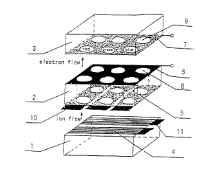
l3rief descriptions of the accompanying figures:
Figure 1 is an overview of the structure of a FID; and
Figure 2 is a partial view of the structure of FID.
The best way to implement the invention:
(n Fig. 1 and 2, the back plate 1 is a field ion emission plate, the cover
plate s is a fluorescent plate, the inner plate 2 between the back plate 1 and
the cover plate 3 is a microchannel plate. The above three plates are all
made oi~ insulating material, for instance, of glass.
Un the inner side of the field ion emission plate l, an X-line electrode
system 4 is provided, each X-line electrode being formed by many (e.g.
several decades) fine wedge shape lines with high curvature, and a thin
4
CA 02332967 2000-11-22
nnetal film is deposited on them. The larger their surface power function the
letter. For example, we can deposit platinum film or graphite-like film on
them to improve their surface work funCt1011.
On the side of the microchannel plate 2 facing the field ion emission
plate l, a Y-line electrode 5 is provided in the direction of the microchannel
holes 8, and an accelerating electrode 6 is provided on the other side.
The crossing points of the Y-line electrodes on the microchannel plate
2 and the X-line electrodes on the field ion emission plate 1 are the
addressing points. On the microchannel plate 2, at every addressing point,
there are plurality of microchannel holes 8 with a diameter of several
decades micro-meters passing through. These microchannel holes have an
angle with the perpendicular line of the microchannel plate, which ranging
f=rom ~ to 20 degrees.
On the inner side is the fluorescent plate s, facing every addressing
point, pixels 9 with three original colors of high-voltage fluorescent
materials are deposited. A thin aluminum film is deposited on them,
forming the screen electl-ode 7.
AS ShOWII 111 Fig. 2, the field ion emission plate 1 and the microchannel
plate 2 are located several a m apart from each other, the microchannel
plate 2 and the fluorescent plate 3 several mm apart, these three plates being
parallel to each other and the microchannel plate 2 being arranged between
:lie other two plates and being peripherally sealed with a thlll gas filled in
as
the imaging gas. The pressure of the gas is 10-4 -:(0-5 tor. We should select
the inert gas with low ionization potential, high negative electron affinity
and low atom number or mixed with a few other gases. All the lead wires of
Uhe electrodes should be kept outside of this device to be connected with the
driving circuits. The overview of the structure of FID is shown in Fig. l, in
~~~IllCh 1711111er1Cal IO represents the lead wires of the Y-line electrodes
on the
microchannel plate 2, and 11 that of the X-line electrodes on the field ion
emission plate 1. This device is addressed with X-~' encoding.
The tl-liclaless of FID is about 5 to 20 mm, determined by the area of
this panel display. On the field ion emission plate l, the X-line electrode
system 4 is fabricated by micro-electronic technologies. The distance
between the centers of two neighboring X-lines arid the width of every X-
line electrode are determined according to the resolution of the display
needed. For example, if the resolution of the display is100 pixels per
~duare mln, then the distance between the central :lines of two neighboring
X-lines should be about 100 ~ m, and the width of each X-line electrode
s
CA 02332967 2000-11-22
Translation of the amended pages of Amendment under Article 41
may be 60 a m. Clearly,the resolution of the display may be 9 pixels per
square mm, Moreover, each X-line electrode comprises over ten paralleled
wedge shape lines (in the width of 1-2 a m), for example, by depositing a
thin metal film on them.
The thickness of the microchannel plate 2 is about 2 mm. On the side
of the microchannel plate 2 facing the field ion emission plate l, the Y-line
electrode system 5 is provided. The distance between the centers of two
neighboring Y-lines and the width of each Y-line equal correspondingly to
that of the X-line electrode system 4. The crossing points of the Y-line
electrodes and the X-line electrodes are the addressing points. Each
addressing point contains a plurality of microchannel holes 8 in the
diameter of 10-50 ~ m. The microchannel holes 8 pass through the
microchannel plate with an angle 5 to 20 degrees perpendicular to the
surface of the microchannel plate 2. On the other side of the microchannel
plate 2, an accelerating electrode 6 is provided.
On the inner side of the fluorescent plate 3, the pixels 9 in three
original colors (red, green and blue) are provided, with each pixel facing
each addressed point vertically. An aluminum film with thickness of 0.1 ~
m is deposited on them as the screen electrode 7, which also serves as a
protecting layer and a reflecting layer for the fluorescent material. The
manufacturing processes are substantially similar to that of CRT.
When an addressed point (Xi, Yj) is applied with bias and signal
voltage, the field ions will be emitted from around the addressing point on
the field ion emission plate 1. These emitted ions are accelerated by the
field and impinged on the wall of the microchannel holes 8, stimulating
multifold secondary electrons emissions, so that the flow is multiplied.
These secondary emission electrons are then accelerated by the accelerating
electrode 6, thus to become a strong electrons flow. After extracting from
the other side of the holes, the strong electrons flow is accelerated again
and
focused by the screen electrode 7, and finally bombard on a corresponding
pixel of the screen. The microchannel plate not only can convert the ion
flow into a strong electrons flow, but also can divide the colors of the
signal
as the shielding plate does in CRT, through which the electron beam can
bombard on the corresponding red, green and blue pixels, thereby
producing a color image.
The inventive FID is filled with thin inert gas (10-4 -10-S tor), so the gas
will not react chemically with other materials inside the FID. Moreover, the
inert gas possesses negative electron affinity, its molecule is easy to loss
an
electron and forming a positive ion. As the electrons are accelerated by the
field and bombard on the fluorescent plate, the positive ions will be
6
CA 02332967 2000-11-22
accelerated on the opposite direction, so that the positive ions cannot
bombard on the fluorescent plate and make damage to it.
In this embodiment, which has a diagonal of 150 mm, the DC
reference voltage of each electrode is:
The X-line electrode system4 on the field ion emission plate l:
+30V-~300V.
The Y-line electrode system 5 on the microchannel plate 2: OV.
The accelerating electrode 6 on the microchannel plate 2: +1000V.
The screen electrode 7 on the fluorescent Plate3: +1000V-~-+6000V.
The device is addressed by X-Y encoding. When the bias and signal
voltage are applied between Xi-line and Yj-line, the gas molecules between
the crossing point of Xi and Yj will be ionized, thereby forming a positive
ion emission flow based on the signal strength.
With the multifold secondary electron emission multiplied of the
microchannel holes 8 and the accelerating voltage applied on them, the
positive ion emission flow become a strong electron flow.
With the high voltage of the screen plate 7, the energy of the strong
electron beam is further increased, to stimulate the high-voltage color
fluorescent material directly.
Using the color dividing function of the microchannel plate 2, color
image display can be realized.
Increasing the diameter of the microchannel holes 8 and increasing the
thickness of the microchannel plate 2 in proportion ( 1:40), so as to increase
the surface area of the microchannel plate, we can :realize large screen FID.
The embodiment is only for the FID with diagonal of 150 mm. If the
diagonal of FID is changed, the above-mentioned parameters should be
amended accordingly.
Industry availability
From the above contents, it can be concluded that FID will find a wide
range of utilization because it is easy to produce, with low cost, high
efficiency and high quality of color image.