Note: Descriptions are shown in the official language in which they were submitted.
CA 02333173 2000-11-15
- 1 -
SPECIFICATION
BS DIGITAL BROADCAST RECEIVER
TECHNICAL FIELD
The present invention relates to a BS digital broadcast receiver,
and more particularly to a BS digital broadcast receiver having a
phase error table to be used for carrier reproduction.
BACKGROUND OF THE INVENTION
A BS digital broadcast system adopts as its modulation scheme
a Trellis coding 8PSK (simply called also Trellis 8PSK) modulation
scheme which is one of coding modulation schemes.
For Trellis decoding by a Viterbi decoder of a conventional BS
digital broadcast receiver, as shown in Fig. 8, baseband demodulation
signals I and Q demodulated from a reception signal converted into
an intermediate frequency signal are supplied to an 8PSK demapper
31 which converts them into tri-bit data (MSB, CSB, LSB) and
supplies them to delay circuits 32 to 34 to delay them. The
baseband demodulation signals I and Q are also supplied to a QPSK
mapping conversion circuit 35. The QPSK mapping conversion
circuit 35 converts the signals I and Q into baseband demodulation
signals I' and Q' of QPSK and outputs them. The QPSK mapping
conversion circuit 35 also outputs I-axis code data and Q-axis code
data representative of the position of a reception signal point to be
used for detecting whether the position of the reception point belongs
CA 02333173 2000-11-15
_ 2
to which quadrant, to delay circuits 36 and 37 to delay them.
The baseband demodulation signals I' and Q' output from the
QPSK mapping conversion circuit 35 are supplied to a Viterbi decoder
40 to Viterbi-decode them and output decoded data which is also
supplied to a convolution encoder 41 to reencode them.
The delay time set to the delay circuits 32 to 34 and delay
circuits 36 and 37 is a total sum of a time taken for the Viterbi
decoder 40 to decode and a time taken for the convolution encoder 41
to reencode.
The tri-bit data (MSB, CSB, LSB) delayed by the delay circuits
32 to 34, the I-axis code data and Q-axis code data delayed by the
delay circuits 36 and 37, and the convolution reencode outputs
(TCD 1, TCDO) are supplied to an MSB code judging/error detecting
circuit 42 which obtains a most significant bit TCD2 and error flags
of Trellis decoding. Demapping means to rearrange mapping of the
relation between a reception signal and its phase.
As described above, for Trellis decoding in the conventional BS
digital broadcast receiver, it is necessary to delay the demapped
tri-bit data and the I-axis code data and Q-axis code data by a time
equal to the total sum of the time for the Viterbi decoder to decide a
path and the time for the convolution reencoding. Five delay circuits
are therefore required.
It is an object of the present invention to provide a BS digital
broadcast receiver capable of dispensing with an 8PSK demapper and
reducing the number of delay circuits used for Trellis encoding.
CA 02333173 2000-11-15
- 3 -
DISCLOSURE OF THE INVENTION
A BS digital broadcast receiver for receiving a Trellis 8PSK
modulation signal, as recited in claim 1 of this invention, comprises:
phase error data generating means for generating phase error
data in accordance with a phase difference between 0 degree and a
phase of a reception signal point position, in order to reproduce a
carrier;
a Viterbi decoder for Viterbi-decoding a QPSK baseband signal
based upon a reception signal point position of an absolute-phased
baseband demodulation signal;
an encoder for convolution-encoding a Viterbi decode output;
delay means for delaying a predetermined number of upper bits
of the phase error data corresponding to the phase difference between
0 degree and the phase of the reception signal point position, by a
total sum of a time taken by said Viterbi decoder to Viterbi-decode
and a time taken by said convolution encoder to convolution-encode;
a demapping conversion circuit for demapping outputs from
said delay means; and
an MSB code judging circuit for outputting a code determined
from an output of said demapping conversion circuit and a
convolution encode output, as an MSB of a Trellis 8PSK decode
output.
According to the BS digital broadcast receiver as recited in
claim 1 of this invention, the QPSK baseband signal based upon a
reception signal point position of an absolute-phased baseband
CA 02333173 2000-11-15
- 4 -
demodulation signal is Viterbi-decoded by the Viterbi-decoder. An
output of the Viterbi-decoder is convolution-reencoded by a
convolution encoder. A predetermined number of upper bits of
phase error data corresponding to a phase difference between 0
degree and a phase of a phase error detection reception signal point
position, is delayed by delay means for carrier reproduction, by a
total sum of a time taken by the Viterbi decoder to Viterbi-decode and
a time taken by the convolution encoder to convolution-encode. The
delayed outputs from the delay means are demapped by the
demapped value conversion circuit. A code determined from the
demapped output and convolution encode output is output as an
MSB of a Trellis 8PSK decode output from the MSB code
judging/error detecting circuit.
Therefore, according to the BS digital broadcast receiver as
recited in claim 1 of this invention, an SPSK demapper conventionally
required can be dispensed with and the number of delay circuits to
be used for Trellis encoding is only the number of delay circuits
predetermined for particular phase error data to thereby reduce the
number of delay circuits.
In the BS digital broadcast receiver as recited in claim 1 of this
invention, the predetermined number of upper bits may be four bits,
the MSB code judging circuit may compare a reception signal point
position on a Trellis 8PSK mapping having lower two bits same as a
Viterbi decode output with an MSB judging demapped value on an
MSB judging circle obtained by rotating the Trellis 8PSK mapping by
CA 02333173 2000-11-15
- 5 -
22.5 degrees, judge a reception signal point position having a shorter
distance as a judged position, and if an MSB of the judged position is
not same as an MSB of the MSB judging demapped value, invert the
MSB of the MSB judging demapped value and outputs the inverted
MSB as a judged MSB.
BRIEF DESCRIPTION OF THE DRAWINGS
Fig. 1 is a block diagram partially showing the structure of a
BS digital broadcast receiver according to an embodiment of the
invention.
Figs. 2(A) to 2(C) are schematic diagrams illustrating
demapping phase error data and a phase error data used by the BS
digital broadcast receiver of the embodiment.
Figs. 3(A) to 3(C) are schematic mapping diagrams illustrating
the arrangement of Trellis 8PSK modulation signal points and MSB
inversion used by the BS digital broadcast receiver of the
embodiment.
Fig. 4 is a diagram illustrating the relation between phase error
data, MSB judging demapped values, and error flag demapped values
used by the BS digital broadcast receiver of the embodiment.
Fig. 5 is a diagram illustrating the relation between MSB
judging demapped values and decided MSB values used by the BS
digital broadcast receiver of the embodiment.
Fig. 6 is a block diagram showing the structure of an MSB code
judging/error detecting circuit of the BS digital broadcast receiver of
CA 02333173 2000-11-15
- 6 -
the embodiment.
Fig. 7 is a block diagram showing the structure of an MSB code
judging circuit of a BS digital broadcast receiver according to another
embodiment of the invention.
Fig. 8 is a block diagram partially showing the structure of a
conventional BS digital broadcast receiver.
EMBODIMENTS OF THE INVENTION
Embodiments of a BS digital broadcast receiver of this
invention will be described.
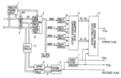
Fig. 1 is a block diagram partially showing the structure of a
BS digital broadcast receiver according to an embodiment of the
invention.
A reception signal converted into an intermediate frequency is
demodulated by a demodulation circuit into 8-bit baseband
demodulation signals I(8) and Q(8) ((8) is the number of quantization
bits which is omitted hereinafter).
The demodulated baseband demodulation signals I and Q are
supplied to an absolute-phasing circuit 1 and a remapper 2. The
remapper 2 makes the reception signal point phase be coincident
with the phase on the transmission side and also makes all reception
points be set to a reference phase, e.g., 0 phase. The
absolute-phasing circuit 1 obtains a current reception phase by
comparing the reception point position of a frame sync signal in the
baseband demodulation signals I and Q with an already know signal
CA 02333173 2000-11-15
- 7 -
point position of a transmission side frame sync signal, and supplies
a first phase rotation signal AR of three bits which signal is used for
making the reception signal point position be coincident with the
transmission signal point position. The remapper 2 rotates the
reception signal phase in a reverse direction by an angle represented
by the first phase rotation signal AR to thereby make the reception
signal phase be coincident with the transmission signal phase.
The baseband demodulation signals I and Q absolute-phased
by the remapper and having the coincident phase with the
transmission signal phase are supplied to a phase error detecting
circuit 3. The phase error detecting circuit 3 generates a second
phase rotation signal CR of three bits representative of a difference
between 0 degree and the reception point phase and supplies it to the
remapper circuit 2. The remapper circuit 2 rotates the baseband
demodulation signals I and Q in a reverse direction by an angle
represented by the second phase rotation signal CR to make the
reception point position be set to 0 degree.
A remapping process of the remapper 2 to make the reception
signal point position be coincident with the position on the
transmission side is executed during the first half period of one
symbol period, and the remapping process to make the phase of the
reception signal point position be set to 0 degree is executed during
the last half period of one symbol period. The absolute-phasing
circuit 1, remapper 2 and phase error detecting circuit 3 have been
already proposed in Japanese Patent Application No. 10-033732
CA 02333173 2000-11-15
submitted by the present applicant.
The absolute-phased baseband signals output from the
remapper 2 are supplied to a latch circuit 4 and latched during one
symbol period synchronously with a symbol clock. Therefore, the
latch circuit 4 continues to output the absolute-phased baseband
demodulation signals I and Q during one symbol period.
The phase error detecting circuit 3 has a phase error table 31
schematically shown in Fig. 2(A). This phase error table 31 stores
therein phase difference data between 0 degree and the reception
signal phase of each of the baseband demodulation signals I and Q.
By referring to this phase error table 31, the phase difference data
between 0 degree and the reception signal phase of each of the
baseband demodulation signals I and Q whose phase was set to 0
degree is obtained and supplied to an AFC circuit to reproduce the
carrier.
The phase error detecting circuit 3 is required to have only one
phase error table 31 which stores the phase error data.corresponding
to the phase difference between 0 degree and the reception signal
phase of each of the baseband modulation signals I and Q
demodulated from a received 8PSK modulation signal. The angle of
0 degree is only illustrative and an optional reference value may be
used. In this case, the phase error table 31 stores the phase
difference between the optional reference value and the reception
signal phase.
The absolute-phased baseband signals I and Q output from the
CA 02333173 2000-11-15
- 9 -
latch circuit 4 are supplied to a QPSK mapping table conversion
circuit 5 and converted into QPSK baseband demodulation signals I'
and Q' in accordance with the signal point arrangement of lower two
bits of the tri-bit data demapped from the reception points. The
QPSK mapping table conversion circuit 5 maps the absolute-phased
baseband modulation signals I and Q into QPSK signals
schematically shown in Fig. 3(B) in accordance with the lower two
bits of the tri-bit data demapped from the reception points
schematically shown in Fig. 3(A). In this manner, the QPSK
baseband modulation signals I' and Q' based on the reception signal
point positions can be obtained.
These converted QPSK baseband modulation signals I' and Q'
are supplied to a Viterbi decoder 6 to be Viterbi-decoded. This
decoded data is supplied to a convolution encoder 7 to be reencoded
and output as encode outputs TCD1 (C1) and TCDO (CO).
The upper four bits (MSB, MSB-1, MSB-2, MSB-3) of the phase
error data of eight bits output from the phase error detecting circuit 3
by referring to the phase error table 31 are supplied to delay circuits
81, 82, 83 and 84, respectively, to be delayed by a total sum of the
time taken for the Viterbi-decoder to decode and the time taken for
the convolution encoder 15 to encode.
The outputs from the delay circuits 81, 82, 83 and 84 are
supplied to a demapped value conversion circuit 9 which generates
an MSB judging demapped value for deciding either 0 or 1 of MSB of
2 5 the Viterbi decode output for the Trellis decoding process and an
CA 02333173 2000-11-15
- 10 -
error flag demapped value for detecting an error. Instead of
supplying the upper four bits of the phase error data to the delay
circuits, they may be directly supplied to the demapped value
conversion circuit and the output of the demapped value conversion
circuit is supplied to delay circuits.
Prior to describing the demapped value conversion circuit 9,
the upper four bits of the output of the phase error table 31 shown in
Fig. 2(A) will be described. If the phase difference between 0 degree
and the phase of the reception signal point of each of the baseband
signals I and Q is in the range from 3 ~r / 2 radian to 0 and to ~r / 2
radian, the value (MSB) of the I-axis is 0 (positive) and MSB of the
phase error data is 1. If the phase difference between 0 degree and
the phase of the reception signal point of each of the baseband
signals I and Q is in the range from ~c / 2 radian to r1 radian to 3 ~r / 2
radian, the value (MSB) of the I-axis is 1 (negative) and MSB of the
phase error data is 0. In Fig. 2(A), MSB-1, MSB-2 and MSB-3 of the
phase error data are represented by binary data of three bits.
The four bits ( a ) of the phase error data are supplied to the
demapped value conversion circuit 9. Areas corresponding to the
upper three bits ( a ) of the phase error data ( a ) are determined as A,
B,..., H as shown in Fig. 2(C) from the upper three bits ( ~ ), as shown
in Fig. 4. The upper three bits ( ~ ) are added to 110. If the lower
two bits of the addition result are 11, these two bits are changed to
10, and if they are 10, they are changed to 11. The addition results
are output as MSB judging demapped values (D2, D 1, DO). With this
CA 02333173 2000-11-15
- 11 -
process, the lower two bits of the MSB judging demapped values (D2,
D 1, DO) become gray codes.
The upper four bits ( a ) of the phase error data are supplied to
the demapped value conversion circuit 9, and the phase error data
( a ) is added to 0001. The upper three bits (S) of the addition data
( y ) are obtained. In accordance with the upper three bits, as shown
in Fig. 4 the areas corresponding to the upper three bits (8) are
determined as a, b,..., h as shown in Fig. 2(B). The upper three bits
(b) are added to 110. If the lower two bits of the addition result are
11, these two bits are changed to 10, and if they are 10, they are
changed to 11. The addition results are output as error flag
demapped values (Trellis 8PSK demapped values (Z2, Z1, ZO)). With
this process, the lower two bits of the error flag demapped values (Z2,
Z1, ZO) become gray codes.
The MSB judging demapped values (D2, D 1, DO) and error flag
demapped values (Z2, Z1, ZO) output from the demapped value
conversion circuit 9 and the reencoded outputs TCD 1 and TCDO from
the convolution encoder 15, are supplied to an MSB judging/error
detecting circuit 10.
In the phase error table shown in Fig. 2(A), corresponding areas
a, b,..., h, A, B,..., H are shown for reference.
For Trellis encoding for 8PSK modulation, MSB of the tri-bit
data is not convolution-encoded but it is output as it is. Therefore, it
is necessary to decide MSB for decoding. For the Trellis 8PSK
mapping shown in Fig. 3(A), an MSB judging circle shown in Fig. 3(C)
CA 02333173 2000-11-15
- 12
as an inner circle is considered which circle is obtained by rotating
the circle shown in Fig. 3(a) by 22.5 degrees in a counter-clockwise
direction.
Consider now, for example, a Viterbi decode result of O1.
Positions 001 and 101 in the Trellis 8PSK mapping both have the
lower two bits of O1 which are the same as the Viterbi decode result.
Therefore, the positions 001 and 101 are used as the MSB candidates
for the Trellis 8PSK mapping. If the MSB judging demapped value is
010, the MSB candidate 101 is nearer to the MSB judging demapped
value 010 than the MSB candidate 001, as indicated by a one-dot
chain line so that 101 is decided as MSB. With this decision, the
MSB judging demapped value is 010, whereas the decided MSB value
is 101. Since both MSBs have different codes, it is necessary to
invert MSB of the MSB judging demapped value 010.
Similarly, if the MSB judging demapped value is 111 for the
Viterbi decode result of O1, the MSB candidate 101 is nearer to the
MSB judging demapped value 111 than the MSB candidate 001, as
indicated by a two-dot chain line so that 101 is decided as MSB.
With this decision, since the decided MSB value for MSB judging
demapped value of 111 is 101, MSB of the MSB judging demapped
value of 11 l and MSB of the decide MSB value of 101 have the same
code. It is not necessary to invert MSB of the MSB judging
demapped value 111.
Whether the code of MSB is required to be inverted or not is
2 5 determined as in the above manner, for each Viterbi decode result
CA 02333173 2000-11-15
13 -
and each MSB judging demapped value. This result is shown in Fig.
S. In Fig. 5, a circle symbol in a change column indicates that MSB
is required to be inverted. The demapped value for which MSB is
required to be inverted is indicated in the square brackets [ J in Fig.
3(B) schematically in correspondence with the Viterbi decode result.
In Fig. 5, the Viterbi decode result is simply indicated as xx, the MSB
judging demapped value is simply indicated as a demapped value,
and the decided MSB value is simply indicated as a decided value.
As shown in Fig. 6, the MSB judging/error detecting circuit 10,
to which the MSB judging demapped values (D2, D l, DO) and error
flag demapped values (Z2, Z1, ZO) output from the demapped value
conversion circuit 9 axe supplied, is constituted of an MSB judging
circuit 111, exclusive logical OR circuits 112, 113 and 114.
As shown in Fig. 7, the MSB judging circuit 111 has: AND gates
211 to 216 to which the MSB judging demapped values (D2, D 1, DO)
for judging MSB required to be inverted are supplied; OR gates 217 to
219 which output data in accordance with the Viterbi decode results;
a selector 220 for selecting one of the outputs from the OR gates 217
to 219 in accordance with the Viterbi decode result; and an exclusive
logical OR circuit 221 for receiving an output from the selector 220
and D2 of the MSB judging demapped values (D2, D 1, DO) and
outputting TCD2 (MSB). TCD2 (MSB) output from the exclusive
logical OR circuit 221 and the decode output from the Viterbi decoder
6 constitute the Trellis-decoded Viterbi decode data. In Fig. 7, TCD 1
and TCDO are convolution-reencoded outputs (C1, CO) from the
CA 02333173 2000-11-15
- 14 -
convolution encoder 7.
The AND gate 211 outputs a high level signal when the MSB
judging demapped value takes 010, the AND gate 212 outputs a high
level signal when the MSB judging demapped value takes 011, the
AND gate 213 outputs a high level signal when the MSB judging
demapped value takes 110, and the AND gate 214 outputs a high
level signal when the MSB judging demapped value takes 111. The
OR gate 217 outputs a high level signal when the AND gate 21 l, 212,
213, or 214 outputs the high level signal, this output being selected
by the selector 220 when the convolution-reencoded outputs (C1, CO)
are 00.
The OR gate 218 outputs a high level signal when the AND gate
211 or 213 outputs the high level signal, this output being selected
by the selector 220 when the convolution reencoded outputs (C1, CO)
are O 1.
The AND gate 215 outputs a high level signal when the MSB
judging demapped value takes 000, and the AND gate 216 outputs a
high level signal when the MSB judging demapped value takes 100.
The OR gate 219 outputs a high level signal when the AND gate 215
or 216 outputs the high level signal, this output being selected by the
selector 220 when the convolution reencoded outputs (C1, CO) are 10.
The high level signal from the selector 220 is inverted in
accordance with the MSB judging demapped value D2 of 0 or 1 and
output as TCD2 of 1 or 0.
As apparent from the foregoing description, in judging MSB,
CA 02333173 2000-11-15
- 15 -
the reception signal point position in the Trellis 8PSK mapping having
the same lower two bits as the encode output of the ~Viterbi code is
compared with the MSB judging demapped value on the MSB judging
circle obtained by rotating the Trellis 8PSK mapping in the
counter-clockwise direction by 22.5 degrees, and if MSB of the judged
position is not the same as MSB of the MSB judging demapped value,
MSB of the MSB judging demapped value is inverted and outputs as
the judged MSB.
The MSB judging circuit 111 outputs an inverted MSB when
the demapped value is required to be inverted as illustrated in Fig. 5.
In this manner, the MSB judging circuit 111 performs Trellis
decoding in cooperation with the Viterbi decoder 6 and convolution
encoder7.
The output TCD2 of the MSB judging circuit 111 and the error
flag demapped value Z2 are supplied to the exclusive OR circuit 112,
the convolution reencoded output CO and error flag demapped value
Zl are supplied to the exclusive OR circuit 113, and the convolution
reencoded output C 1 and error flag demapped value ZO are supplied
to the exclusive OR circuit 114. Error flags are output from the
exclusive OR circuits 112 to 114.
The exclusive OR circuits 112 to 114 can output the error flags
because one input to each of the exclusive OR circuits 112 to 114 is
equal to the input for the convolution encoding and if it is not
coincident with each of the error flag demapped values Z2 to Z0, a set
2 5 bit is output.
CA 02333173 2000-11-15
- 16 -
INDUSTRIAL APPLICABILITY
As described so far, according to the BS digital broadcast
receiver of this invention, an 8PSK demapper conventionally required
can be dispensed with, and the number of delay circuits to be used
for Trellis encoding is only the number of delay circuits
predetermined for particular phase error data to thereby reduce the
number of delay circuits.