Note: Descriptions are shown in the official language in which they were submitted.
CA 02333498 2001-02-O1
LASER DIODE MODULE
BACKGROUND OF THE INVENTION
1. Field of the Invention
The present invention relates to a semiconductor laser
module that is used for optical communication and so on.
2. Description of the R.e.lated Art
A development of a high power semiconductor laser module
as an exciting light source and the like in an amplifier for an
optical fiber that .:is used f:or optical communication is in progress.
A conventianal sern_iconductor laser module comprises, as is
shown in Fig. 6, for example, a semiconductor laser device 1, an
optical fiber 2 that receives laser light emitted from the
semiconductor laser device 1 and a photo diode 3 that monitors
optical output of the semiconductor laser device 1. These
semiconductor laser device l, optical fiber 2 and photo diode 3
are housed in a package 10.
The semiconductor laser device 1. is optically coupled at
its front facet la (emi.tting facet) side with the optical fiber
2 and is confronted at :its rear facet lb (re:flecting facet) side
with the photo diode 3. An anti-reflection coating film whose
reflectance is, for example, around several percent is provided
on the front facet la of the semiconductor laser device 1 and a
1
CA 02333498 2001-02-O1
reflection coating film whose reflectance is, for example, around
90 percent is provided on the rear facet. lb.
The semiconductor laser device 1 is fixed to a base (a base
part) 6 via a heat sink 9 and a fixing part 5, and the photo diode
3 is fixed to the base 6 by a photo diode fixing part 8.
In the semi. conductor laser modules shown in Fig. 6, ferules
lla, 11b are provided while keeping a distance from each other in
the lengthwise direction of the optical fiber 2, which is inserted
and fixed in these ferules 11a, llb. The ferule lla functions as
a means for supporting the optical fiber and is made of a Kovar
(Trade mark) that is a Fe-Ni-Co alloy, for example.
The base 6 is fixed on a thermomodule 7 and the thermomodule
7 is mounted on a bottom board l0a of the package 10. Here, as is
shown in Fig. 6, the thermomodule 7 genera.Lly comprises a base--side
board 17, a bottom board--side board 18 and a peltier cooler (a
peltier device) 19 pinched between these boards 17 and 18. Both
the base-side board 17 and the bottom board-side board 18 of the
thermomodule 7 are made of A1203. And the ferule llb is fixed to a
side-wall of the package 7_0.
In the above mentioned semiconductor laser module, the
semiconductor 1 and the opt:=ical fiber 2 are aligned, and laser .Light
emitted from the front facet la of the semiconductor laser device
1 is received by the optical fiber 2 to be transmitted in the opi=ical
fiber 2 and is provided for a desired use.
2
CA 02333498 2001-02-O1
Further, in the above mentioned semiconductor laser module,
an optical output from the rear facet 1b of the semiconductor laser
device 1 is monitored by the photo diode 3, thereby the optical
output from the front facet la of the semiconductor laser device
1 is controlled. In other- words, the output from the emitting facet
of the optical fiber 2 is controlled by controlling the laser output
based on the monitoring of the photo diode 3.
Here, as the above mentioned semiconductor laser module
monitors the optical out=put from the rear facet lb of~ the
semiconductor laser device 1 by the photo diode 3, it is needed
to permit light having a certain intensity to be emitted from the
rear facet lb of the semiconductor laser device 1 and to reach to
a light receiving surface of the photo diode 3. For that purpose,
normally, the reflectance of the rear facet lb of the semiconductor
laser device 1 is reduced to a certain extent, for example, to 90
percent or less, intentionally.
However, when the reflectance of the rear facet lb
(reflecting facet) of the semiconductor laser device 1 is reduced,
there exists a problem in that an optical output form the front
facet la of the semiconductor laser device 1 decreases to reduce
the optical output from the semiconductor laser module itself.
In recent years, another constitution for a semiconductor
laser module has been proposed in which a fiber grating is provided
on the optical fiber 2 of 1=he semiconductor laser module. The fiber
3
CA 02333498 2001-02-O1
grating functions as a diffraction grating reflecting only .Light
having a predetermined wavelength out of the laser beams that are
emitted from the semiconductor laser device 1 and enter the optical
fiber 2. Thus, the output= wavelength of the semiconductor :Laser
module is stabilized by providing the diffraction grating, such
as a fiber grating, on the optical fiber 2.
However, in this constitution, as the polarization
direction of the reflected light selected by the diffraction grating
on the basis of the wavelength fluctuates by the change o:E the
positional condition of th,e optical fiber 2, a returning light with
a changed polarization di=rection is returned to the semiconductor
laser device 1 from the front facet la of the semiconductor .Laser
device 1 through the optical fiber 2, when the positional condition
of the optical fiber 2 is changed. The power of the optical out=puts
from the front facet 1a and rear facet lb of the semiconductor. .Laser
device 1 thus fluctuates. In particular, the amount of the
fluctuation of the optical output by the above mentioned disturbance
in the case of light emitted from the rear facet lb of the
semiconductor laser device 1 is bigger than that in the case of
light emitted from the front facet la.
Accordingly, when the fiber grating is provided on the
optical fiber 2 of the sern:iconductor laser device 1 shown i.n Fig.
6, it has been difficult to precisely conduct APC (Automatic :Power
Control) for controlling optical output from the front facet la
CA 02333498 2001-02-O1
of the semiconductor laser device 1 to a fixed value. Namely, in
the constitution shown in figure 6, when the fiber grating is
provided on the optical fiber 2 and the output light from the rear
facet lb of the semiconductor laser device 1 is monitored, the
fluctuation of monitor current is so large that it was impossible
to control the optical output from the front facet la of the
semiconductor laser device 1 to a fixed value.
SUMMARY OF THE INVENTION
The present. invention has been made to solve the above
mentioned problems, and an object of the present invention therefore
to provide a high power semiconductor laser module that can control
the optical output to a fixed value.
In order to achieve the above-mentioned object, the present
invention provides a semiconductor laser module with the following
constitution.
According to a fi.r:~t constitution of the present invention,
there is provided a semiconductor laser module comprising: a
semiconductor laser device; an optical fiber that receives laser
light emitted from the semi.c:onductor laser device; and a photo diode
monitoring an optical output of the semiconductor laser device,
characterized in that the photo diode monitors an optical output
of the semiconductor laser device by receiving scattered light at
a laser light receiving end of the optical fiber.
CA 02333498 2001-02-O1
A sem_iconductor_ laser module according to a second
constitution of the present invention is characterized in that the
reflectance at a facet opposite side to the optical fiber of the
semiconductor laser device is set to 95 percent or more, in addition
to the above mentioned first constitution.
Further, a semiconductor laser module according to a third
constitution of the present invention is characterized in that the
laser light receiving end of the optical fiber is formed into a
lens, in addition to the above mentioned first constitution.
Further, a semiconductor laser module according to a forth
constitution of the present invention is characterized in that light
emitted from the semiconductor laser_ device is optically coupled
to the laser light receivz.ng end directly, in addition to the above
mentioned first (third) constitution.
Further, a semiconductor laser module according to a fifth
constitution of the present invention is characterized in that the
laser light receiving end is formed into a wedge-shaped lens, in
addition to the above mentioned third constitution.
Further, a semiconductor laser module according to a sixth
constitution of the present invention is characterized in that the
optical fiber includes a diffraction grating reflecting only light
having a predetermined wavelength out of laser beams that are
emitted from the semiconductor laser device and incident to the
optical fiber, in addition to the above mentioned first
J
CA 02333498 2001-02-O1
constitution.
Further, a semiconductor laser module according to a seventh
constitution of the pre~~ent invention further comprises a base on
which the semiconductor laser_ devise is mounted, and is
characterized in that the optical fiber is placed such that a plane
bisecting the wedge angle of the wedge-shaped lens is parallel to
the base and that the phot=o diode is placed under the wedge-shaped
lens, in addition to the above mentioned fifth constitution.
Further, a semiconductor laser module according to an eighth
constitution of the pre sent invention further comprises a base on
which the semiconduct:.or laser devise is mounted, and is
characterized in that the optical fiber is placed such that a plane
bisecting the wedge angle of the wedge-shaped lens is perpendicular
to the base and that the photo diode is placed on a flank portion
side of the laser light receiving end having the wedge-shaped lens,
in addition to the above mentioned fifth constitution.
Further, a semiconductor laser module according to a ninth
constitution of the present invention further comprises: a base
on which the semiconductor laser device and the optical fiber are
mounted; a fixing means :fvor fixing the optical fiber to the base;
a thermomodule on which the base is mounted; and a package housing
the photo diode, the sem:ic:onductor laser device, the optical fiber,
the fixing means, the base and the thermomodule, and is
characterized in that: the thermomodule is mounted on a bottom board
CA 02333498 2001-02-O1
of the package; the the:rmomodule includes a base-side board, a
bottom board-side board and a pettier cooler pinched between these
boards; the base is composed of a laser device mounting member that
is in contact with the the:rmomodule to mount the semiconductor laser
device, and a fixing means mounting member that is placed. on a
position outside a semiconductor laser device mounting region of
the laser device mounting member to mount the fixing mean;; and
the laser device mounting member is made of a material having a
coefficient of linear expansion within the range between the
coefficient of linear expansion of the fixing means mounting member
and the coefficient of 1_inear expansion of the base-side board of
the thermomodule, in addition to the above mentioned first
constitution.
Further, a semiconductor laser module according to a tenth
constitution of the present invention further comprises a base on
which the semiconductor laser device and the optical fiber are
mounted, and is characterized in that: the optical fiber is fixed
to the base while being pinched by a fixing means from both flank
portion sides; a package is provided for housing the photo diode,
the semiconductor laser device, the base and the fixing means; a
thermomodule is mounted on a bottom board of the package; the base
is mounted on the thermomodule; a fixing means mounting portion
mounting the fixing means is provided on the base; a first
laser-welded portion formed by laser-welding the fixing means
CA 02333498 2001-02-O1
mounting portion and t:he fixing means and a second laser-welded
portion formed by lase.r--welding the fixing means and an optical
fiber supporting means are provided; and the first laser-welded
portion and the second laser-welded portion are made t:o have
approximately the same heights in the direction perpendicular to
the bottom board of the package, in addition to the above mentioned
first constitution.
Further, a semiconductor laser module according to an
eleventh constitution o:f the present invention further comprises:
a base mounting the semi.c:onductor laser device and the optical
fiber; a fixing means for fixing the optical fiber to the base;
and a thermomodule mounting the base, and characterized in that
wall portions are provided on the base at the both side of the frank
portionsof an optically-coupled portioninterposed between a.laser
light-emitting facet of the semiconductor laser devise and a :Laser
light receiving end of the optical fiber, in addition to the above
mentioned first constitution.
Further, a semiconductor laser module according to a twelfth
constitution of the presE'Ilt invention further comprises: a base
mounting the optical fiber and the semiconductor laser device; a
thermomodule mounting tlne base; and a package housing the photo
diode, the semiconductor laser device, the optical fiber, the base
and the thermomodule, and i.s characterized in that: the thermomodule
is mounted on a bottom board of the package; the thermomodule
9
CA 02333498 2001-02-O1
includes a base-side board, a bottom board-side board and pE'ltier
cooler pinched between these boards; and the difference bE:tween
the coefficient of linear_ expansion of base-side board and bottom
board-side board and the coefficient of linear expansion of the
bottom board of the pac~:age is 1X10⁻⁶/K or less, in addition t:o the
above mentioned first constitution.
In the present invention according to the above mentioned
(first) constitution, a reflection surface is provided at the laser
light receiving end of the optical fiber and the photo diode receives
laser light (scattered light) reflected at the laser light receiving
end of the optical fiber and monitors the optical output of the
semiconductorlasermodule.Thereforthesemiconductorlasermodule
according to the present invention does not need to emit light from
the rear facet of the serniconductor laser device (the facet on the
side opposite to the optical fiber side) , unlike the conventional
modules.
Accordingly, the semiconductor laser module according to
the present invention aan increase the optical output of the
semiconductor laser device and increase the optical output o:f the
semiconductor laser module itself, as the reflectance at the rear
facet of the semiconductor laser device can be increased.
Namely, the semi.conductor_ laser module according ~-c> the
present invention can, as in the above mentioned second constitution,
increase the reflectance <~t the facet of the semiconductor laser
CA 02333498 2001-02-O1
device on the side opposite to the 'optical fiber to, for example,
95 percent or more, and can be a semiconductor laser module that
can achieve a stable and high output.
As the third constitution of the present invention is
provided with a lens ( for example, wedge-shaped lens or spherical
lens) at the laser light receiving end of the optical fiber and
the laser light is optically coupled to the lens-like laser light
receiving end, the efficiency in collecting light from the
semiconductor laser device can be improved and the output of the
semiconductor laser module can be increased even more.
Further, when thE~~ _L.ight emitted from the semiconductor laser
device is optically coupled to the laser light receiving end
directly, as in the forth constitution of the present invention,
the improvement of the light coupling efficiency from. the
semiconductor laser device of the above mentioned third
constitution is achieved effectively.
When the laser Eight receiving end is formed :into a
wedge-shaped lens, as i.n the fifth constitution of the pr~ssent
invention, the processing becomes relatively easy and the module
can be applied, with a good collecting efficiency, even to a
semiconductor laser device whose emission intensity distribution
at its facet is not isotropic (for example, is elliptic) . Further,
with this constitution, the laser light c:an be reflected at. slant
surfaces of the wedge-shaped lens at the laser light receiving end
17
CA 02333498 2001-02-O1
of the optical fiber, and the inclination of the slant surfaces
is large. Therefor, the separation distance between the light
emitted from the semiconductor .laser device and received a.t the
laser light receiving end of the optical fiber and the scattered
light that is the refleci~:ion of the received light can be small.
Accordingly, in this constitution, the photo diode can be placed
in the vicinity of the lensed fiber and the layout design is easy,
even when a semiconductor laser device chip carrier and so on are
placed together.
Further, i.n the semiconductor laser module, with a
constitution in which, for example, a diffraction grating, such
as, a fiber grating reflecting only light having a predetermined
wavelength out of all t}ne laser beams is provided on the cptical
fiber, the oscillation wavelength of the semiconductor laser module
can be stabilized.
However, in the constitution in which a diffraction grating
is provided on the optical fiber, although the laser output
wavelength can be stabilized, there exists a possibility of
generating return light, whose reflected light from the diffraction
gratingfluctuates in its intensity or whose polarization direction
fluctuates. Then, in the constitution that a diffraction grating
is provided on the optical fiber, the optical output of the
semiconductor laser device fluctuates . Even in this case, however,
the fluctuation of the optical output emitted from the semiconductor
~2
CA 02333498 2001-02-O1
laser device to the opt~.cal fiber is smaller than the fluctuation
of the light emitted from the rear facet of the semiconductor laser
device. Accordingly, the .semiconductor laser module of the present
invention can easily be controlled by APD control, even when it
has the constitution that. the diffraction grating is provided on
the optical fiber.
Further, by placing the optical fiber such that the plane
bisecting the wedge angle of the wedge-shaped lens is parallel to
the base mounting the semiconductor laser device and by placing
the photo diode under t:he wedge-shaped lens, as in the seventh
constitution of the present invention, the reflected light at the
laser light receiving end of the optical fiber can be received and
monitored effectively by the photo diode.
Further, by placing the optical fiber such that the plane
bisecting the wedge angle of the wedge-shaped lens is perpendicular
to the base mounting the semiconductor laser device and by placing
the photo diode on the frank portion side of the laser .Light
receiving end of the wedge-shaped lens, as in the eighth
constitution of the present invention, the reflected light at the
laser light receiving end of the optical .fiber can be received and
monitored effectively by the photo diode, as in the case of the
seventh constitution.
Further, in the present .invention, with the constitution
that the base mounting the semiconductor laser device ano'~ the
13
CA 02333498 2001-02-O1
optical fiber comprises the laser devise mounting member and fixing
means mounting member, and the laser device mounting member .i~> made
of a material having a coefficient of linear expansion within the
range between the coefficient of linear expansion of the fixing
means mounting member and the coefficient of linear expansion of
the base-side board of the thermomodule mounting the base,, the
following effect can be obtained.
Namely, with this constitution, even when the thermomodule
is bent due to a temperature change of the semiconductor laser module,
the warp of the base can be relieved and the deterioration of
efficiency of the optical coupling between the semiconductor .Laser
device and the optical fiber due to the temperature change o:f the
working environment can be restrained. Further, as the fluctuation
of the light monitored by t:he photo diode (the reflected light from
the optical fiber) is re~;trained, this constitution can provide
a stable and high power semiconductor laser module.
Further, in the present invention, by setting the difference
between the coefficient c>f linear expansion of the base-side board
and the bottom board-side board and the coefficient of linear
expansion of the bottom board of the package to 1 X 10⁻⁶ /K or less,
the deterioration of efi-iciency of the c>ptical_ coupling between
the semiconductor laser device and the optical fiber due to the
temperature change of the working environment can be restrained,
and a more stable and high power semiconductor laser module can
19
CA 02333498 2001-02-O1
be obtained.
Further, in the present invention, with the constitution
that the first laser-welded portion, which is formed by welding
the fixing means mounting portion of the base and the fixing means
for fixing the optical fiber supporting means with laser, and the
second laser-welded portion, which is formed by welding the fixing
means and the optical fiber supporting means with laser, have
approximately the same hE=_ight in the direction perpendicular to
the bottom board of the package, the effect described below can
be obtained.
Namely, with this constitution, even if the base is warped
to a certain extent, the position of the optical fiber supporting
means does not largely deviate with the first laser-welded portion
functioning as a fulcrum, and accordingly, the deterioration of
the efficiency of the optical coupling between the semiconductor
laser device and the optical fiber can be effectively restrained
and the fluctuation of monitoring value by photo diode can be
restrained as well.
Further, in the present invention, with the constitution
that wall portions are pro>vided on the base on both side of: the
frank portions of an optically-coupled portion interposed between
a laser light-emitting facet of the semiconductor laser devise and
a laser light receiving end of the optical fiber, the effect
described below can be obtained.
1~~
CA 02333498 2001-02-O1
Namely, with this constitution, as the warp of the base at
the optically-coupled portion between the semiconductor laser
device and the optical fiber can be restrained by the wall portions,
the deterioration of the efficiency of the optical coupling between
the semiconductor laser device and the optical fiber can be
effectively restrained and the fluctuation of monitoring value of
light monitored by the photo diode can be restrained as well.
BRIEF DESC'~tIPTION OF THE DRAWIN
Exemplary embodiments of the invention will now be described
in conjunction with the drawings in whir_h:
Fig. 1 is a sectional side view of a semiconductor .Laser
module according to a first embodiment of the present invention;
Fig. 2A is <~ front view of an end of an optical fiber used
in the first embodiment of- the present invention and Fig. 2.B is
a side view of the end of the optical fiber used in the first
embodiment of the present invention;
Fig. 3 is a sectional plan view of a semiconductor laser
module according to a second embodiment of the present invention;
Fig. 4 is a sectional side view of a semiconductor laser
module according to a third embodiment o_f the present invention;
Fig. 5A is perspective view illustrating the constitution
of the periphery of a base according to a forth embodiment of- the
present invention and Fig. 5B is a sectional view illustrating the
16
CA 02333498 2001-02-O1
vicinity of a coupled portion of a semiconductor laser device with
the optical fiber according to the forth embodiment of the present
invention.
Fig. 6 is a sectional side view of a conventional semiconductor
laser module.
DETAILED DESCRIPTTON OF THE PREFERRED EMBODIMENT
Embodiments of the present invention will now be described
in detail with reference to the drawings.
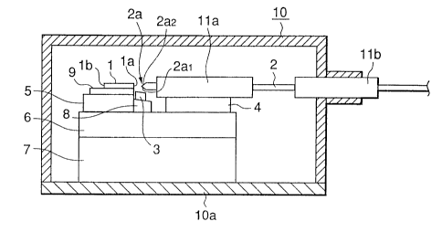
Fig. 1 is a sectional side view of a semiconductor laser
module according to a first embodiment of the present invention.
In Fig. l, identical reference numbers are used to indicate the
parts having names identical with those in the conventional model
shown in Fig. 6, and the explanation thereof is omitted or
simplified.
In Fig. l, the opti_ca1 fiber 2 is a so-called tensed fiber,
which is provided with a lens at its tip (having its tip processed
into a lens) . The laser light receiving end 2a of the optical fiber
2 is, as shown in Figs. 2B and 2B, formed into a wedged shape. The
slant surfaces constituting the lens are composed of the reflac:tion
surfaces 2a1 and 2a2 that have an effect of a lens collecting laser
light and reflect a part of the received 7_aser light. A radius of
curvature R of the laser 1_ight receiving end 2a of the optical fiber
2 is, for example, 3 to 10 ~m and a wedge angle B is around 60 degree.
17
CA 02333498 2001-02-O1
As mentioned above, the optical fiber 2 with the laser light
receiving end 2 having a wedge-shaped lens can reflect a part of
the output light of the semiconductor laser_ device 1 at: the
reflection surfaces 2a, and 2a~ without impairing the optical
coupling with the semiconductor laser 1 largely.
In this embodiment., the optical fiber 2 is placed such that
a plane (imaginary plane) H bisecting the wedge angle 8 of: the
wedge-shaped lens is parallel to the base 6, and is fixed on the
fixing part 4 via the ferule lla. And the photo diode 3 is p7_aced
under the wedge-shaped lens, i.e. at the opposing side to the
reflecting surface 2a1.
The present embodiment is characterized, as opposed to the
conventional model, in that the photo diode 3 directly receives
the scattered light reflected at the laser light receiving end 2a
of the optical fiber 2 and monitors the optical output of the
semiconductor laser device= 1. Namely, in the present embodiment,
the photo diode 3 is provided in the vicinity of a region under
the end portion 2a of the optical fiber 2, and light emitted from
the front facet la (emit;t.ing facet) of the semiconductor laser
device 1 is partially reflected at the reflection surface 2a1 that
is the lower side end surface of the laser light receiving end 2a
of the optical fiber 2, and the reflected light is received by the
photo diode 3.
In this embodiment, with this constitution, as it is no :more
18
CA 02333498 2001-02-O1
needed to emit light for monitoring from the rear facet lb
(reflection facet) of the semiconductor laser device 1, the
reflectance of the rear facet lb of the semiconductor laser device
1 is set to 95 percent o:r more.
The constitution of this embodiment other than those
described above is ident~ic:al with the conventional semicondvuctor
laser module illustrated in Fig. 6, and the semiconductor .Laser
module according to the present embodiment receives the laser :Light
emitted from the front facet la of the semiconductor laser device
1 with the optical fiber_ 2 and transmits the same in the opi=ical
fiber 2, as in the conventional semiconductor laser module. However,
in the present embodiment, the photo diode 2 receives the optical
output reflected at the reflection surface 2a1 of the laser light
receiving end 2a of the optical fiber 2 and monitors the oot:ical
output of the semiconduca or laser device 1.
Thereafter, the semiconductor lasermodule accordingto the
present embodiment controls the optical output of the semiconductor
laser device 1 based on the result of the monitoring. Therefore,
the semiconductor laser module according t:o the present embodiment
does not need to emit 1_ight from the rear facet lb of the
semiconductor laser device 1 as conventionally. Accordingly, in
the semiconductor laser module according to the present embodiment,
as it is possible to set t;he reflectance of the rear facet lb to
95 percent or more, or preferably to 100 percent, it is possible
19
CA 02333498 2001-02-O1
to increase the optical c>utput of the semiconductor laser device
1 and to increase the output of the semiconductor laser module
itself.
In this embodiment, as the wedge-shaped lens is provided
in the laser light receiving end 2a of the optical fiber 2 and the
lens portion is largely slanted, the separation distance between
the light emitted form the semiconductor laser device 1 and the
above mentioned scattered light to be monitored by the photo diode
3 can be small. Accordingly, the photo diode 3 can be placed in
the vicinity of the optical fiber 2 and layout design can be simple,
even when, for example, the photo diode 3 is placed with LD chip
carrier and so on.
Since the reflect_Lon surfaces 2a1 and 2az are provided in
the wedge-shaped lens, the light is strongly scattered toward the
reflection direction of these surfaces (vertical direction, in this
case). Accordingly, the .Light with sufficient intensity can be
monitored by the photo diode placed under the lens.
Further, as this embodiment employs a constitution in which
the laser light is coupled directly to the lensed fiber (optical
fiber 2) that is provided with the wedge-shaped lens at the laser
light receiving end 2a, the collection efficiency of the light form
the semiconductor laser device 1 and the output power of the
semiconductor laser module can be increased even more.
Further, in the pr_~esent embodiment, as the shape of the lens
CA 02333498 2001-02-O1
at the laser light receiving end 2a of the optical fiber 2 is a
wedged shape, it can be processed relatively easy and the laser
module can be applied , with good collection efficiency to the
semiconductor laser device 1 whose light emission intensity
distribution is not isot:ropic(for example, elliptic).
Fig. 3 shows a sectional plan view of a second embodiment
of the semiconductor laser module according to the present invention.
In the second embodiment, identical reference numbers are used to
indicate parts identical caith those in -the first embodiment and
the explanation thereof is not repeated.
The second embodiment is constituted almost in the same way
as the above-mentioned first embodiment. The second embodiment is
characterized, as opposed to the first embodiment, in that. the
optical fiber is placed ~;uch that the plane (imaginary plane) V
bisecting the wedge angle ~9 of the wedge-shaped lens of the optical
fiber is perpendicular to the base 6, and that, in accordance with
this constitution, the photo diode 3 is placed in the vicinit=y of
a flank portion of the laser light receiving end 2a having the
wedge-shaped lens.
In the second embodiment, similar to the first embodiment,
the slant surfaces of the wedge-shaped lens of the optical fiber
2 is made.to serve as the reflects_on surfaces 2a1 and 2a2, and the
photo diode 3 opposes the reflection surface 2a1.
The second embodiment can provide similar effects with
?_.1
CA 02333498 2001-02-O1
similar functions to the first embodiment.
Fig. 4 shows a sectional side view of a third embodiment
of the semiconductor laser device according to the present invention.
In the third embodiment, identical reference numbers are used to
indicate the parts identical with those in the first embodiment
and the explanation thereof is not repeated.
The third embodiment is constituted almost in the same way
as the above mentioned first embodiment, and the third embodiment
is characterized, as opposed to the first embodiment, in that a
fiber grating 12 is provided on the optical fiber 2. The :fiber
grating 12 functions as a diffraction grating reflecting only .Light
with a set wavelength out of the light beams that are emitted from
the semiconductor laser device 1 and enter the optical fiber 2.
The third embodiment is constituted as described above and
the third embodiment can provide similar effects through similar
operations to the first embodiment.
Since the semiconductor laser module according to the third
embodiment is provided with the fiber grating 12 on the optical
fiber 2, the output. wavelength of the semiconductor laser me>dule
2 can be stabilized.
Here, when the dif_=:racoon grating, like the fiber grating
12 and so on, is provided as in the third embodiment, there exists
a possibility of generating return light whose reflected light from
the diffraction grating functions in its intensity or whose
22
CA 02333498 2001-02-O1
polarization direction fluctuates. The return light as such causes
the optical out put from the semiconductor laser device 1 to
fluctuate. However, even in the case, as the amount of the
fluctuation of the optical. output emitted from the semiconductor
laser device 1 toward the optical fiber 2 i.s smaller than the amount
of the fluctuation of the light emitted from the rear facet: lb of
the semiconductor laser device, it is easy to conduct the APC control
and a stable optical output can be obtained, in the third embodiment .
The main constitution of a forth embodiment of the
semiconductor laser module according to the present invention is
shown in a perspective view in Fig. 5A, and the constitution of
a portion in the periphery of the optically-coupled portion between
the semiconductor laser device 1 and the optical fiber 2 :in the
semiconductor laser module according to the forth embodiment is
shown as a sectional side view in Fig. 5B.
Here, in the forth embodiment, identical reference numbers
are used to indicate the parts identical with those in the first
embodiment, and as the constitutions of the semiconductor laser
device l, the optical fiber 2, the package 10 and the ferule llb
in the forth embodiment are identical to those in the embodiment
l, the explanations thereof is not repeated. In the forth embodiment
also, as is shown in Fig 5B, the photo diode 3 is provided =~n the
vicinity of the laser light receiving end 2a of the optical fiber
2 the photo diode 3 is omitted from the illustration of Fig. 5A.
23
CA 02333498 2001-02-O1
The characteristics of the forth embodiment different from
the first embodiment are the constitution of the base 6 and the
constitution for fixing the optical fiber to the base 6. In the
forth embodiment, the fluctuation of the reflected light ate the
laser light receiving end 2a of the optical fiber 2 due to the bent
of the module is restrained by the following constitution and the
constitution is appropriate to prevent the fluctuation of the light
monitored by the photo diode 3.
In the present embodiment, the base 6 is constituted ao as
to comprise a laser device mounting member 20 mounting the
semiconductor laser device 1 and a fixing means mounting member
21, and fixing means 26, 2 7 are mounted on the fixing means mounting
member 21. The fixing means 26 and 27 are for fixing the optical
fiber 2 via the ferule lla, and are placed while keeping a distance
from each other in the optical axis direction.
As is shown in F:ic(. 5B, the laser device mounting rnember
20 is placed on the thermomodule 7 and is in contact with the
thermomodule 7, and the thermomodule 7 is mounted on the bottom
board l0a of the package .LO. The bottom board l0a of the package
is made of a CuWlO (the weight ratio of Cu is 10 percent and that
of W is 90 percent), which i.s a Cu-W alloy.
An LD bonding portion 24 that .is composed of a common member
with the laser device mounting member 20 is mounted on the upper
side of the laser device mounting member 20 to constitute a
24
CA 02333498 2001-02-O1
semiconductorlaser devicemounting region.Thesemiconductorlaser
device 1 is mounted on the LD bonding portion 24 via the heat sink
(chip carrier) 9. And a thermistor 50, which detects the temperature
of the vicinity of the semiconductor laser device 1, is mounted
on the LD bonding portion 24. The temperature control by the
thermomodule 7 is conducted based on the temperature information
from the thermistor 50.
The fixing means mounting member 21 is mounted on the 1_aser
device mounting member 20 at a location outside of the semiconductor
laser device mounting region, and the fixing means mounting member
21 is fixed on the laser device mounting member 20 using wax or
the like.
The fixing means mounting member 21 is made of a Kovar, and
the laser device mounting member 20 is made of a CuWlO (the weight
ratio of Cu is 10 percent and that of W is 90 percent), which is
a Cu-W alloy.
Here, the CuWlO has the thermal conductivity of 180 to 200
(W/m~K) which is ten times higher than that of the Kovar, which is
17 to 18 (W/mK). On the other hand, the Kovar is a metal having
low thermal conductivity, good laser-welding property and a
coefficient of linear expansion similar to the optical fiber 2.
In the forth embodiment, there are provided the first
laser-welded portion 15, which is made by laser-welding the fixing
means mounting member 21 as a fixing means mounting portion and
CA 02333498 2001-02-O1
fixing means 26, 27, and the second laser-welded portion 16, which
is made by laser-welding the fixing means 26, 27 and the ferule
11a. The first laser-welded portion 15 and the second laser-wE=_lded
portion 16 are formed to have about the same height in the direction
perpendicular to the bottom board l0a of the package (the difference
between these heights is within ~ 500~m, preferably within ~50 ~tm) .
Namely, the first and second laser-welded portions 15, 16 are made
to align practically on a common plane.
At least on the fixing means 26 side, of the first and second
laser-welded portions 15, 16 have almost the same height as the
center of the optical fiber (the ridge line at the tip of the lens
2, here).
The alignment between the semiconductor laser device 1 and
the optical fiber 2 is clone at the time of fixing the ferule lla
at the first and second :laser-welded portion 15, 16. For example,
to begin with, a side of the ferule lla close to the semiconductor
laser device 1 is aligned, and is fixed to the fixing means :?6 at
the second laser-welded portion 16. Then the side of the ferule
lla remote from the semiconductor laser device 1 is moved and al~_gned
as is shown as a in Fig. 5A with the second laser-welded portion
16 of the fixing means 26 as a fulcrum utilizing the leverage.
Afterward, by fixing the ferule lla at the second laser-welded
portion 16 on the fixing means 27, the optical fiber 2 and the
semiconductor laser dev:ic:e 1 are aligned and fixed precisely.
26
CA 02333498 2001-02-O1
Further, in the forth embodiment, wall portions 25 as a means
for preventing warp are provided on the fixing means mounting m~smber
21 of the base 6 on both s_Ldes of the frank portions of the optical
fiber 2 along the lengthwise direction of the optical fiber 2. The
wall portions 25 are for preventing the base from warping, and,
in the forth embodiment, ~>tand on the bottom portion of the faxing
means mounting member 21 upwardly.
In the present embodiment, the wal:L portions 25 are provided
on the entire region in the lengthwise direction of the fixing means
mounting member 21, and t:he fixing means 26, 27 are provided in
grooved regions between t:he wall portions 25.
The front ends of the wall portions 25 expand toward a region
where the LD bonding portion 24 of the laser device mounting member
20 is placed. With this constitution, the wall portions 2_'i are
provided on both sides o:f the frank portions of the optically-
coupled portion interposed between the emitting facet 1a of laser
light of the semiconductor laser device 1 and the laser light
receiving end 2a of the optical fiber 2, in order to make it possible
to restrain the positional displacement of the optically-coupled
portion of the semiconductor laser device 1 and the optical fiber
2.
The forth embodiment is constituted as mentioned above, and
in the forth embodiment, the optical fiber 2 is placed such that
the plane (not shown in the figures) bisecting the wedge ang:Le of
2 '7
CA 02333498 2001-02-O1
the wedge-shaped lens o:f the optical fiber 2 is parallel to the
base 6 and the photo diodes 3 is placed on the opposing side o:f the
lower reflection surface 2a1 of the wedge-shaped lens, as in the
first embodiment. Therefore, the forth embodiment can provide
effects similar to the first embodiment and a stable and high power
output can be obtained.
And in the forth embodiment, the base 6 is composed o:f the
laser device mounting member 20, which is in contact with the
base-side board member 17 of the thermomodule 7, and the fixing
means mounting member 21 provided thereon. And the laser device
mounting member 20 is made of a material having a coefficient of
linear expansion (5.8 - 6.5 X 10⁻⁶/K) wit:hin a range between the
coefficient of linear expansion of the fixing means mounting member
21 ( 5 . 3 X 10⁻⁶/K) and that of the base-side board 17 ( 6. 5 X 10-''/K) .
Namely, in the present embodiment, as the laser device mounting
member 20 is made of CuWlO having a coefficient of linear expansion
within the range between t:hose of Kovar and A1203, the warp of the
base 6 due to the temperature change of the working environment
is relieved, compared to the case where the base 6 made of ~:ovar
is placed on the base-side board 17 made of A1z03 with direct contact.
And in the present embodiment, as i:he coefficient of linear
expansion of the base-side board 17 and the bottom board-side board
18 (made of A1.03) is extremely close to that of the bottom board
l0a of the package (the difference in coefficient of linear
2. ~3
CA 02333498 2001-02-O1
expansion among them is 1 . () X 10-~/K or less) , the warp of the bottom
board of the package can be prevented.
And the CuWlO, which is used to form the laser device
mounting member 20, h.as excellent thermal conductivity,
specifically ten times bigger than that of a Kovar. Therefor, with
the forth embodiment, the heat generated in the semiconductor laser
device 1 can be transferr_~ed effectively to the thermomodule 7 side
via the heat sink 9 and the laser device mounting member 20, and
the semiconductor laser device 1 can be cooled down by the
thermomodule 7 effectively.
Further, in the forth embodiment, the first laser-welded
portion 15 and the second laser-welded portion 16 are formed to
have approximately the same height. Therefore, with the forth
embodiment, even when the base warps to a certain extent, the ferule
11a does not make a large positional displacement with the
laser-welded portion 15 functioning as a fulcrum by the warp.
Further, in the forth embodiment, by providing the wall
portions 25 on both sides of the frank portions o:f the
optically-coupled portion interposed between the emitting facet
(front facet) la of the laser light of the semiconductor laser device
1 and the laser light rece:eiving end 2a of the optical fiber 2, along
the lengthwise direction of the optical fiber 2, the warp of the
base 6 at the optically coupled portion of the semiconductor laser
device 1 and the optical fiber 2 is restrained.
29
CA 02333498 2001-02-O1
As mentioned above,, with the forth embodiment, as the amount
of the deterioration of the optical coupling efficiency between
the semiconductor laser device 1 and optical fiber 2 and fluctuation
of the amount of the monitoring value of the photo diode can be
restrained, even when the temperature of the working environment
changes, a semiconductor laser device with even more stables and
high power output can be obtained.
Here, the present invention is not limited to the above
mentioned embodiments and is applicable to various other models.
For example, the shape of the laser light receiving end 2a of: the
optical fiber 2 is not 1i_mited to those mentioned in the above
embodiments, and can be comical or spherical. In the case that: the
laser light receiving end is shaped into a conical or spherical
shape, as these shapes are symmetrical with respect to the center
axes, the location where the photo diode 3 is placed is not limited
to a particular location around the laser light receiving end 2a.
Namely, the photo diode 3 can be placed on any suitable location
around the laser light receiving end 2a. And the optical fiber 2
is not necessarily limited to a lensed fiber with its front end
is processed.
Also, it is preferable for the surface of the laser light
receiving end 2a to be coat=ed so that the light is scattered less .