Note: Descriptions are shown in the official language in which they were submitted.
CA 02333509 2001-02-01
Exress Mail N EL353512279tJS
System and Method for tJsing Multiple Lead Connections in an Electropolishing
Process
"Thomas A. Lorincz
BACKGROLJNL) OF THE INVENTION
ield of the Invention:
This invention relates generally to electropolishing processes, and more
particularly to a
system and method for electropolishing, tlre inner surface of a pipe. Even
more particularly, the
present invention relates to a system and method for maintaining process
parameters (e.g., the
electrode-pipe gap voltage within acceptable limits.
Description of the Background Art:
FIG. 1 is a block diagram of a typical electropolishing system 100 for
polishing the inner
surface of a pipe 102. Electropolishing system 100 includes a power a power
supply 104 having
a first voltage supply terminal 106 and a second voltage supply terminal 108,
a cable 1 10, an
electrode 112, and an electrical lead 114. Electrode 112 is coupled to first
voltage supply
terminal 112 via cable l 10, and pipe 102 is coupled to second voltage supply
terminal 108 via
electrical lead 114. An electrolyte solution (rlot shown) is circulated
through pipe 102 during the
electropolishing process by an electrolyte pumping system (not shown).
Power supply 104 asserts a first voltage, via first voltage supply terminal
106 anci cable
I 10, on electrode 112, and a second voltage, via second voltage supply
terminal 108 and
electrical lead 1 14, on pipe 102. "fhe voltage difference between electrode
112 and pipe 102
causes electrical current to flow frorn electrode 112, through the electrolyte
solution (e.g.,
phosphoric acid or sulfiiric acid solution), to pipe 102. "fhe electrical
current selectively removes
microscopically raised points froni the inrier surface of pipe 102 (including
any deposits
thereon), into the electrolyte solution in the form of a soluble salt,
effectively polishing the inner
surface of pipe 102.
The amount of electrical current, and thus the amount of material removed from
the inner
wall of pipe 102, depends on the voltage difference between electrode 112 and
pipe 102. When
electrode 112 is in position W, close to the connection between pipe 102 and
lead 114, the
resistance of pipe 102 is negligible, so that the voltage ciifference between
electrode 112 and pipe
102 is essentially equal to the voltage difference between first supply
terminal 106 and second
CA 02333509 2001-02-01
supply terminal 108. However, during the electropolishing process, electrode
112 is drawn
through pipe 102 from position W to position X, to position Y, and finally to
position Z. As
electrode 112 is drawn away from position W the resistance of pipe 102 becomes
a factor,
reducing the voltage difference between electrode 122 and pipe 102. The
changing voltage
between electrode 112 and pipe 102 results in the nonuniform electropolishing
of the inraer
surface of pipe 102.
FIG. 2 is a chart 200 showing the increased resistance of pipe 102, and the
associated
change in voltage across the electrolyte gap, as electrode 112 is drawn
through pipe 102. The
electrode positions (W, X, Y, Z) shovvn in chart 200 correspond to the
positions illustrated in
FIG. 1. The resistance (R) of pipe 102 wa.s determined by the equation:
R=p(D/A), (Cq- 1)
where R is the resistance of pipe 102, p is the resistivity of'the material of
which pipe 102 is
constructed, L is the ler.igth of pipe between the particular position and
position W, and A is the
cross-sectional area of pipe 102. For purposes of this example, p is taken as
2.362 micro-ohms
per foot, the resistivity of type 304 stainless steel, and the cross-sectional
area of pipe 10:2 is
.9655 square feet. The voltage drop (V) tlirough a particular section of pipe
102 is calculated
using Ohm's law:
V=IR, (Eq. 2)
where (I) is the process current and (R) is the resistance of the relevant
section of pipe 102.
The voltage between electrode 112 anu pipe 102 (the gap voltage) is determined
by
subtracting the voltage drop across the particular pipe section from the
voltage between first
supply terminal 106 ancl second supply terrriirial 108 (the process voltage).
Chart 200 shows that
as the distance between electrode 112 and the junction between pipe 102 and
lead 114 (position
W) increases, the gap voltage decreases. The decreasing gap voltage results in
the nonuniform
electropolishing of the inner surface of pipe 102.
What is needed is an electropolishing systern anci nlethod, wherein the gap
voltage may
Ee maintained within a desired range to achieve the unifomi electropolishing
of the inner surface
cf a pipe.
2
CA 02333509 2001-02-01
SUMMARY
The present invention overcomes the problems associated with the prior art by
providing
a novel system and method for unifoc-nily electropolishing the inner surface
of a pipe. 'The
invention helps maintain the process voltage within a desired range by
utilizing a plurality of
electrical leads to achieve uniform electropolishing of the pipe. Coupling the
pipe to a common
voltage source with a plurality of electrical leads reduces the electrical
resistance through the
pipe by reducing the length of pipe through which the current must flow.
The embodiment of the present invention includes an electrode for placement
within the
pipe, a plurality of electrical leacis, and a power supply having first and
second voltage supply
terminals. Each of the electrical leads is adapted to electrically couple a
separate portion of the
pipe to a common voltage source. The second voltage supply terminal of the
power supply is
also adapted to couple to the common voltage source. A cable electrically
couples the electrode
with the first voltage supply terminal of the power supply and draws the
electrode through the
pipe. In a particular embodiment the common voltage source is ground. In a
more particular
embodiment the electrical leads and/or the second voltage supply terminal of
the power supply
are adapted to facilitate separate grounding.
In another embodiment the plurality of electrical leads are adapted to couple
to a single
common voltage source, and in a more particular ernbodiment, the electrical
leads are ernbodied
in a single, electrically conductive cable. In an alternate embodinlent, each
of the electrical leads
comprises an electrically conductive cable with a first end adapted to couple
to the pipe to be
electropolished and a second end adapted to couple to the conlmon voltage
source (e.g. a water
pipe, grounded machinery, etc.). In a particular enibodiment the first end of
each of the leads is
stripped of insulation amd wrapped around the pipe to be electropolished.
Alternatively, the first
end of each of the leads includes a cl,:rmp for electrically engaging the pipe
to be electropolished.
In another particular enlbodiment the second end of each of the leads is
stripped and wrapped
around the common voltage source. AIter-natively, the second end of'each of
the leads includes a
clamp for electrically engaging the cc:ininlon voltage source.
A method for electropolishing the iriner surface of a pipe is also disclosed.
The method
includes steps for placing an electrode within the pipe, attaching the pipe to
a common voltage
source with a plurality of electrical leads, coupling the electrode to the fii-
st voltage supply
3
CA 02333509 2001-02-01
terminal of a power supply, coupling the common voltage source to a second
voltage supply
terminal of the power supply, and drawing the electrode through the pipe.
In a particular inethod the sp,-icing between the electrical leads is
dependent on the
resistivity (p) of the pipe material and an acceptable variation in the
voltage (OVgaP) between the
electrode and the pipe. In a more particular embodiment the spacing (L)
between each of the
leads is obtained by the equation L<_ (4A AVgaP)/(pl) where (I) is the process
current and (A) is
the cross sectional area of the pipe. Optionally, the leads are equally
spaced.
According to one method, the comrnon voltage source is maintained at ground.
Optionally, each of the leads, and/or the second voltage supply terminal of
the power supply are
separately grounded.
In a particular method, the step of attaching the pipe to the common voltage
source
includes attaching each of the leads to a single commori voltage source.
According to another
step of attaching a plurality of electrical leads to the pipe includes
attaching separate portions of
a single, conductive cable to associated portions of the pipe.
In another particular method, the step of attaching the pipe to the common
voltage source
with a plurality of electrical leads includes attaching the first end of each
of the leads to the pipe
and attaching the second end of each of the leads to the common voltage
source. A more
particular method for attaching the leads to the pipe includes wrapping an
uninsulated fii-st end of
each of the leads around the pipe, or ,-1lternatively clamping the first end
of each of the leads to
the pipe. A particular r.nethod for coupling each of the leads to a common
voltage source
includes wrapping an uninsulated second end of each of the leads around the
common voltage
source, or alternatively clamping the second end of each of the leads to the
common voltage
source.
4
CA 02333509 2001-02-01
BRIEF DESCRIPTION OF THE DRAWINGS
The present invention is described with reference to the following drawings,
wherein like
reference numbers denote substantially similar elements:
FIG. 1 is a block diagram showing a known electropolishing system;
FIG. 2 is a table showing the variation of resistance and pipe voltage as the
distance
between the electrical lead and electrode of FIG. I increases;
FIG. 3 is a block diagram showing an electropolishing system in accordance
with the
present invention;
FIG. 4 is a circuit diagram showing a portion of the process current path in
the
electropolishing system of FIG. 3;
FIG. 5 shows an. electrical lead coupled to a pipe according to the present
invention;
FIG. 6 shows a clamp for coupling of an electrical lead with a pipe in
accordance with the
present invention;
FIG. 7 is a block: diagram of an alternate electropolishing system according
to the present
invention; and
FIG. 8 is a block. diagram of another alternate electropolishing system
according to the
present invention.
CA 02333509 2001-02-01
DETAILED DESCRIPTION
The present invention overcomes the problems associated with the prior art by
maintaining the gap voltage (the voltage drop between the electrode and the
pipe) in an
1-'lectropolishing system within a desired range to achieve uniform polishing
of the inner surface
of a pipe. In the following description, numerous specific details are set
forth (e.g. multiple
methods for electricallv engaging an electrical lead with the common voltage
source or with the
pipe to be electropolish.ed) in order to provide a thorough understandirrg of
the inventiorr. Those
skilled in the art will recognize, however, that the inverition may be
practiced apart froni these
specific details. In other instances, details of well known electropolishing
practices (e.g. type
and concentration of the electrolyte solution, particular process voltages,
etc.) have been omitted,
so as not to unnecessari.ly obscure the present invention.
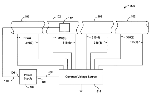
FIG. 3 is a block diagram of an electropolishing system 300 for polishing the
inner
surface of pipe 102. Electropolishing system 300 includes a power supply 104
having a fir-st
Nroltage supply terminal 106 and a second voltage supply terminal 108, a cable
1 10, an electr-ode
12, a common voltage source 314 and a plurality of electrical leads 316(1 to
n). Electrical leads
;l 16 (1 to n) each include a first end for electrically coupling to pipe 102
and a second end for
electrically coupling to common voltage source 314. Electrode 112 is
electrically coupled to
first voltage supply terminal 106 of power supply 104 via cable 1 10. Power
supply 104 is
electrically coupled via cable 320 to common voltage source 3 14. In this par-
ticular embodiment,
common voltage source 314 is maintained at ground.
As used herein, the term "common voltage source" is understood to include any
object
that can serve as a potential reference. For example, objects that may serve
as common voltage
source 314 include, but are not limited to, a grounded piece of industrial
ecluipment, a grounded
building frame, a single conductive cable, or any other object that will serve
as a convenient
reference voltage source.
Power supply 104 asserts a first voltage (with respect to common voltage
source 3 14), via
first voltage supply terniinal 106 anci cable 110, on electrode 112. A second
voltage is asserted
on pipe 102 by common voltage source 314 via electrical leads 316(1) through
316(n). The
voltage difference between charged electrode 112 and pipe 102 causes an
electrical current to
flow from electrode 1 12'., through the electrolyte (not shown), to pipe 102.
As electrode 112 is
6
CA 02333509 2001-02-01
pulled through pipe 102 by cable 1 10, electrical leads 316(1 to n) maintain
the gap voltage
between electrode 112 and pipe 102 within a desired range by reducing the
length of pipe 102
through which the current must flow. Electrical leads 316(1 to n) are spaced
at intervals
c',etermined to regulate the gap voltage at electrode 112 in a desired range
that provides uniform
electropolishing. In this particular embodiment, each adjacent pair of
electrical leads 316(1 to n)
are equally spaced. Those skilled in the art will recognize, however, that
variation in the spacing
of associated pairs of electrical leads 316 (1 to n) is tolei-able, so long as
the gap voltage is
niaintained within the desired range.
FIG. 4 shows a circuit diagram 400 for process current flow through an
adjacent pair of
electrical leads in electropolishing systern 300. Circuit diagrarn 400
includes a cross sectional
portion of pipe 102, cable 1 10, electrode 112, electrical leads 316(1) and
316(2), a resistor 414
representing the gap resistance, and resistors 416 (R 1) and 418 (R2),
represeriting the resistance
ttrrough the respective portioris of pipe 102.
During the electropolishing process power supply 104 asserts a voltage, via
cable 1 10, on
electrode 112. The voltage difference between electrode 112 and common voltage
source 314
causes current to flow between electrode 112 and comrnon voltage source 314.
Assuming the
resistance of leads 316(1) and _316(2) is negligible, the electrical
resistance between electrode
1 12 and common voltages source 314 is the sum of gap resistance 414 and the
total resistance
through pipe 102. For a relatively constant gap resistance 414, the ainount of
current, and
therefore the gap voltage, depends ori the total pipe resistance. When
electrode 112 is near a lead
attachment, the resistance of pipe 102 is negligible. As the electrode 112
moves away from the
point of lead attachment, the increased pipe resistance results in a voltage
drop (Vp;pe) through
pipe 102. Because the voltage betweerl electrode 112 and common voltage source
314 is equal
to the sum of the gap voltage (Vgap) and the voltage drop (Vpõpe) through pipe
102, the pipe
voltage (Vp;pe) must be maintained at or below the acceptable variation in gap
voltage.
For a known acceptable gap voltage (Vgap) range, the spacing (L) between
adjacent
electrical leads 316(1) and 316(2) can be determined as f ol lows. The voltage
drop through pipe
I G2 (Vp,P,) is equal to the product of the process eurrent (I) and the pipe
resistance Rp,pe as given
by Ohm's Law:
VP1pe== I Rpipe (F-q.3)
7
CA 02333509 2001-02-01
The resistance RP;,,, of pipe 102 is equal to the resistance of resistors
416(Ri) ancl
418(R2), in parallel. The first resistance (R 1) represents the section of
pipe 102 between
electrode 112 and electrical lead 316(I), and the second resistance (R2)
represents the section of
pipe 102 between elect:rode 112 and electrical lead 316(2). The total pipe
resistance of pipe 102
(RPiPe) is therefore given by the following equation for parallel resistors:
RiR2
Rn;Pe = -- (Eq. 4).
Ri+Rz
Substituting Equation 4 into Equation 3 yields:
RiR2
Vp;Pe = I - -- (Eq. 5).
RI+R2
The resistance of a particular section of pipe is given by the following
equation:
pD
R =_ -- (Eq. 6).
A
wherein (p) is the resistivity of pipe 102, (D) is the distance between
electrode 112 and one of
electrical leads 316, and (A) is the cross sectional area of pipe 102.
Substituting Equation 6 into Equation 5 for each of resistances R, and R2
yields:
[(PDi)/A] [(PDz)/A]
VP;Pe == I -- - - -- - (Eq. 7).
[(PD,)/A] + [(PD2)/A]
wherein (Di) is the associated length of pipe 102 between electrode 1 12 and
lead 316(1), (D2) is
the associated length of pipe 102 between electrode 112 and lead 316(2), (p)
is the resistivity of
pipe 102, and (A) is the cross sectional area of pipe 102.
Simplifying equation 7 yields:
[(PDiD2)]
VP;Pe = I _- ------- (Eq. 8).
[(Di + Dz)A]
The maximum voltage drop (\/P;,pe) througll pipe 102 occurs when Di = D2
(i.e., when
electrode 112 is halfway between leads :316(1) and 316(2). When Di = D2 then
D, = D2 == (L/2),
8
CA 02333509 2001-02-01
wherein (L) is length between electrical leads 316(1) and 316(2). Substituting
(L/2) for I) , and
D2 in Equation 8 and simplifying yields:
ILp
VPip<: (Eq. 9).
4A
The voltage drop (VPir,,) through pipe 102 must be mairrtaiiled at or below
the maxirnum
acceptable change in the gap voltage (nVgaP). Therefore:
ILp
AVgap < -- --- (Eq. 10).
4A
Solving for L yields:
4A(AVgap)
L < -. (Eq. 1 1)-
pI
Finally, for a given pipe resistivity (p), pipe cross-sectional area (A),
process current (I),
arid maximum acceptable variation in the gap voltage (OVgaP ), the maximum
spacing (L)
between two adjacent leads 316(n) and 316(n+1) can be determined from Equation
11.
FIG. 5 is an axial view of a pipe '502 showing one particular method for
electrically
cciupling an electrical lead 504 to pipe 502. Electrical lead 504 includes a
conductive wire 505
(e.g. solid core or multistrand copper) covered by an insulating sheath 506. A
portion of
insulating sheath 506 is removed from a terminal portion 508 of lead 504.
Terminal portiori 508
is then wound about pipe 502, to establish an electrical connection between
lead 504 and pipe
502, thus providing a path for the electropolishing process current.
While this particular method is particularly simple and convenient, those
skilled iri the art
will recognize that care must be taken to insure that both wire 505 and the
exterior surface of
pipe 502 are clean so as to facilitate a highly conductive connection.
Optioiially, an electrically
conductive paste may be applied to the connection to reduce undesirable
electrical resistance.
Wire 505 should be wrapped tightly around pipe 502, and the rigidity of wire
505 should be
sufficient to niaintain good contact between pipe 502 and lead 504.
The illustrated method is suitable for electrically coupling lead 504 to the
pipe to be
electropolished, as well as to the common voltage source. Pipe 502 is
understood, therefore:, to
9
CA 02333509 2001-02-01
represent either the pipe to be electropolished, or a component of common
voltage source 314
(e.g., a cold water pipe, a grounded safety rail, etc.) in electropolishing
system 300.
FIG. 6 is a side view of aclamp 600 electrically coupling an electrical lead
604 to a pipe
602. Pipe 602 is understood to represent either the pipe being
electropolished, or a component of
common voltage source 314.
Clamp 600 includes a pair of offset arms 606, held in scissor-like
relationship with one
another by a pivot pin 607. One end of each of arms 606 work together as clamp
handles, and
t:ae opposite ends of each of arms 606 work together as clamp jaws. At least
one of the clamp
jaws includes an electrically conciuctive. insert 608 for electrically
erigaging pipe 602. Lead 604
is electrically coupled to insert 608 by a solder joint 610. Clarnp 600
further includes a biasing
member 612 (e.g., a spring) disposed to exert outward pressure on the handle
portions of arms
606, thus providing a clamping force berween jaw insert 608 and pipe 602.
FIG. 7 is a block diagram of art alternate electropolishing system 700
according to the
present invention. System 700 is similar to system 300, except that each of
electrical leacis
316(1-n) and second supply terminal 108 of power supply 104 are separately
grounded (i.e.,
common voltage source 314 is the earth). System 700 has the advantage that
leads 316(1-n) can
be attached to any convenient source of g.round (e.g., grounde(i machinery,
cold water pipe,
grounded building frame, etc.). Thus, leads 316(1-n) can be relatively shorter
in length, because
they only need reach the nearest, most convenient source of ground.
FIG. 8 is a block diagram of an alternate electropolishing system 800
according to the
present invention. System 800 is similar to system 300, except that each of
electrical leacis
316(1-n) are embodied in a single elec.ti-ically conductive cable 802 that is
connected to second
voltage supply terminal 108 of power supply 104, tlninsulated portions 804(1-
n) of cable 802
electrically engage (by wrapping, claniping, or the like) associated portions
of pipe 102.
The description of particular emt~odiments of the present invention is now
complete.
Many of the described features rnay be suhstituted, altered or oniitted
without departing fi-om the
scope of the invention. For example, alternate electrical leads (e.g.,
aluminum conductors), may
be substituted for the copper leads disclosed. These and other deviations from
the particular
ernbodiments shown will he apparent to those skilled in the art, particularly
in view of the
foregoing disclosure.