Note: Descriptions are shown in the official language in which they were submitted.
CA 02333573 2000-11-28
WO 99/63640 PCT/GB99/01693
-1-
POWER-FACTOR CORRECTION ARRANGEMENT
The invention relates to a power-factor correction arrangement in which an
active
source of variable inductance and a passive source of capacitance are
switchably disposed in
parallel across a source of AC power, the passive device being arranged to be
switched into
circuit after the active device.
One example of a known power-factor correction arrangement is shown in Figure
1
and is based on the disclosure of UK patent GB 2,167,582 filed in the name of
the General
Electric Company plc and published on 29 May 1986. In this arrangement a
source of AC
power, e.g. an 11kV bus 10, feeds in parallel through respective AC circuit
breakers 11, 12
and 13 a pair of loads 14, an active source of variable inductance 15 and a
filter bank 16.
These items involve conventional three-phase circuits, though only one phase
is shown in the
diagram. The loads in this example are constituted by a pair of DC motors 17
fed from a pair
of thyristor convertors 18 which in turn are supplied with power from the bus
via
transformers 19. The variable-inductance source 15 comprises essentially a
passive inductor
20 connected to a pair of series-connected thyristor bridge convertors 21
which in turn are
fed from the separate secondaries of a transformer 22. The convertors control
the firing of
the thyristors by way of a multipulse output such as to provide in the stage
15 a current of
variable lagging phase, this current flowing through the AC power bus 10. The
filter bank 16
is in three stages, each designed to attenuate a particular harmonic of the AC
source
frequency but also to provide at that source frequency a net capacitive
reactance, i.e. the filter
appears as a leading-phase branch across the supply 10.
In one mode of operation of this arrangement, the filter 16 is arranged to
provide
leading current to fully compensate the full-load lagging reactive power of
the loads 14. At
less than full load, however, the capacitors in the filter bank 16
overcompensate and would
give rise to a net leading reactive power in the system, were it not for the
fact that the
variable-inductance stage 15 is arranged to provide further lagging VARs (volt-
amps
reactive) to make up for the shortfall of lagging VARs in the motors. Thus,
the lagging
current in stage 15 and that in the load combine at all values of loading to
equal the leading
current in the filter bank 16, thereby giving rise to a substantially unity
power factor.
SUBSTITUTE SHEET (RULE 26)
CA 02333573 2000-11-28
WO 99/63640 PCT/GB99/01693
-2-
In an alternative, and commonly employed, mode of operation the filter bank is
switchable by additional circuits (not shown) between different values of
capacitance such as
to provide incremental changes in leading VARs to suit widely differing load
conditions, the
variable-inductance stage 15 then being controlled as before to provide zero
net power factor,
In other circumstances (for example, when the loads 14 are not in use for a
significant period)
the filter stage may need to be switched out of circuit together with the
stage 15 in order to
save energy. When the filter stage is switched in, there is found to occur a
large pulse of
current through the filter, followed by a large voltage surge which affects
the filter
components, the w=aveform of the AC power source and all other circuits
connection to the
bus 10. These surges can cause significant stress to the filter capacitors and
other circuits and
lead to the necessity to limit the switching rate of the filter stage 16 to a
rate which is
unacceptably low.
Waveforms relating to the power-factor correction arrangement just described
are
shown in Figure 2. In Figure 2, at a time 1.09s approximately, the filter
breaker 13 is closed,
giving rise to a period in which a surge current 40 flows through the filter.
Figure 2 shows
the three AC currents flowing into the filter stage which all start at the
approximately 1.09s
point. There will be three corresponding AC voltage in the AC power system 10,
but only the
worst-affected of these is shown to aid clarity. At the same point in time,
the supply voltage
waveform 41 experiences a pronounced dip 42, followed approximately I Oms
later by a large
voltage rise 43 amounting to an approximately 54% increase over normal peak
voltage levels.
One known way of dealing with the undesirable current surge is illustrated in
Figure
3. In Figure 3 the AC circuit breaker 13 is bypassed by a resistor 23 in
series with an
additional AC circuit breaker 24. Now, when the filter bank is due to be
switched (it is
assumed that breaker 12 is closed), breaker 24 is closed with breaker 13 open,
so that the
filter stage 16 is connected to the supply via the resistor 23, this serving
to reduce the current
surge. A short time later, breaker 13 is closed to fully energise the filter
stage. A drawback
with this approach, however, is the need for the further circuit breaker 24
(there will be one
per phase). This component is not only expensive, it also takes up space and
may in practice
be difficult to retrofit on an existing control panel.
SUBSTITUTE SHEET (RULE 26)
CA 02333573 2007-01-26
21003-2
3
In a second known technique for minimising filter
current pulses during switching, the standard circuit
breaker 13 is replaced by a special device having three
independent contacts, or poles, operated by a special
control arrangement. In operation, when the filter is to be
switched into circuit, the first two poles are closed when
the supply voltage is at a zero value and the third is then
closed a few milliseconds later. Waveforms analogous to
those of Figure 2 but relating to this technique are shown
in Figure 4. This figure shows the point of closure 44 of
the first two poles and that of the third (45) very shortly
afterwards. In Figure 4 only that voltage waveform is shown
which is worst affected (43). The waveform which causes the
poles to close at 44 is not shown. It can be seen that,
though the levels of the current and voltage surges are
reduced when compared with the basic arrangement of
Figure 1, they are still quite appreciable.
While this second technique is partially effective
in reducing the undesired surges through the filter, it
requires the use of an expensive, non-standard circuit
breaker which, as in the case of the first solution, may be
difficult to accommodate in already existing control
equipment.
In accordance with the present invention, there is
provided a power-factor correction arrangement, comprising
an active source of variable inductance and a passive source
of capacitance, the active and passive sources being
connected in parallel to a source of AC power by way of
respective first and second switching means, the arrangement
being configured to close the second switching means while
the first switching means is in a closed state, thereby
drawing a surge electrical current through the passive
source, the active and passive sources being interconnected
CA 02333573 2007-01-26
21003-2
3a
at their switched ends by means of a resistance which
resistance is operative for reducing the surge electrical
current to protect the passive source.
Preferably, the resistance is chosen to have a
value such that a magnitude of a current in the passive
source during a closed state of the first switching means
suffers substantially no change following closure of the
second switching means.
The passive source may be constituted by one or
more capacitors in combination, being either effectively
pure capacitance or an inductance-capacitance combination
forming a filter arrangement.
CA 02333573 2000-11-28
WO 99/63640 PCT/GB99/01693
-4-
The active source may be constituted by, for example, a thyristor-controlled
reactor
or a pair of series-connected multipulse thyristor bridges.
An embodiment of the invention will now be described, by way of example only,
with
reference to the drawings, of which:
Figure 1 is a schematic diagram of a known power-factor correction arrangement
subject to undesirable current and voltage filter-switching surges;
Figure 2 is a waveform diagram showing the existence of current and voltage
surges
in the arrangement of Figure 1;
Figure 3 is a schematic diagram showing a prior-art technique for reducing the
surges
experienced in the arrangement of Figure 1;
Figure 4 is a waveform diagram showing the effect of a second prior-art surge-
reducing technique;
Figure 5 is a schematic diagram of a power-factor correction arrangement in
accordance with the invention;
Figures 6a, 6b, 7a, 7b and 8a, 8b are waveform diagrams illustrating the
effect on
current and voltage, respectively, of the surge-reducing resistance provided
by the power-
factor correction arrangement of Figure 5 for three different values of that
resistance, and
Figure 9 gives details of a typical protection arrangement for incorporation
into the
power-factor correction arrangement according to the invention; many
variations are,
however, possible.
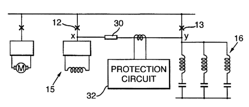
A solution of the present invention to the current and voltage-pulse problem
is
illustrated in Figure 5 and comprises the connecting of a resistance 30 (which
may in practice
be constituted bv a single resistor or a combination of resistors) between the
variable-
inductance stage 15 at the point where it connects to the circuit breaker 12
and the filter stage
= 25 16 at the point where it connects with the circuit breaker 13. The value
of the resistor 30 is
chosen to be such as to minimise surges in the filter when the breaker 12 is
closed, followed
by breaker 13. The exact value depends on the particular AC system involved,
its power
rating, etc.
SUBSTITUTE SHEET (RULE 26)
CA 02333573 2000-11-28
WO 99/63640 PCT/GB99/01693
-5-
A set of waveforms of filter current and AC busbar 10 voltage for an 11 kV, 30
MW
power system as modelled in a simulation routine are shown in Figures 6, 7 and
8 for three
different values of resistor 30, namely 8Ohm, 4 Ohm and 2 Ohm (the resistors
in all three
phases are equal). In each case it is assumed that initially, during a period
T 1(see Figure 6a),
the circuit breakers 12 and 13 associated with the variable-inductance-stage
15 and filter
stage 16, respectively, are open; during a period T2 the circuit breaker 12 is
closed, but
breaker 13 is still open and, lastly, during an open-ended period T3 breaker
13 is closed. It
can be seen how, in the 8 Ohm case, there is a marked discontinuity when
breaker 13 is
closed, the very condition which is to be avoided. However, for smaller values
of resistance
the discontinuity is considerably reduced, so that at 2 Ohm the current and
voltage surges are
negligibie. The actual resistance value decided on depends on the amount of
surge which can
be tolerated, and in this instance either 2 Olun or 3 Ohm might well be the
preferred value.
A marked feature of this inventive arrangement is that, since resistors 30
(considering
all three phases now) are only intended to pass current for a very short time,
e.g. of the order
of 1 second, they can take the fonm of inexpensive generally low-power
devices, provided
they have an adequate surge capability. The exact power rating will depend on
the duty cycle,
which will vary from system to system. In some systems the filter may only be
switched once
every, say, 3 weeks, whereas in other systems switching may be far more
frequent, even every
10 niinutes or so. Even if the switching frequency is as frequent as in the
latter case, the duty
cycle is still low enough to enable inexpensive resistors to be used.
In practice, the integrity of the resistors in the various phases will
normally be
monitored by means of a protection circuit such as that shown at 32 (see
Figure 5). Figure
9 illustrates this in more detail. In Figure 9 the protection circuit
comprises in the same
housing 40 the three resistors 30A, B and C for the three phases and, in the
respective lines
feeding those resistors, associated current transformers 33A, B and C. The
outputs of the
current transformers are taken to a monitoring section 34 which monitors,
among other
things, the open-circuiting of any one resistor in the group of three (i.e.,
loss of current in one
of the phases), and the levels of current in the resistors with respect to
time.
SUBSTITUI'E SHEET (RULE 26)
CA 02333573 2000-11-28
WO 99/63640 PCT/GB99/01693
-6-
The monitoring section 34 conveniently takes the form of a known protective
"black
box" relay which gives a trip output when I2t (a measure of the power
dissipated over time
t, where I is the current) is more than a first predetermined value, or the
instantaneous current
is more than a second predetermined value, or there is a loss of any one or
more of the
phases. An example of a protective relay suitable for such duty is the MIDOS
(Modular
Integrated Drawout System) protective relay marketed by ALSTOM T&D PROTECTION
& CONTROL LTD., St Leonards Works, Stafford ST17 4LX, England.
An analysis of the power-factor protection arrangement shows that it can be
implemented safely, the various fault scenarios being as follows (see Figure
5):
= Circuit breaker 12 goes open - this is an inherently safe condition.
= Short-circuit from point X to ground - circuit breaker 12 is arranged to
trip
(open).
= One resistor 30 goes open-circuit - a phase imbalance is detected and
breaker 12
is tripped.
= One resistor 30 goes short-circuit - a virtually impossible scenario, but is
protected by instantaneous protection anyway, then breaker 12 is tripped.
= Short-circuit from point Y to ground - this is detected by the instantaneous
protection, then breaker 12 is tripped.
= Circuit breaker 13 fails to close - the predetermined 12t setting is
exceeded and
breaker 12 is consequently tripped.
= Circuit breaker 12 trips while the circuit is in operation - the breaker 13
is
arranged to be tripped as well.
= Circuit breaker 13 trips while running - the breaker 12 is arranged to be
tripped
as well.
A summary of the advantages of the power-factor correction arrangement
according
to the present invention is as follows:
(1) Reduced stress on the filter capacitors and all circuits on the AC bus,
due to
negligible current and voltage surges.
(2) Inexpensive, generally low-power, short-time rated resistors can be used.
SUBSTITUTE SHEET (RULE 26)
CA 02333573 2000-11-28
WO 99/63640 PCT/GB99/01693
-7-
(3) Frequent filter-switching operations are possible, enabling the use of the
filter to
be optimised.
(4) No additional standard AC circuit breaker is required; alternatively, no
special
circuit breaker required.
(5) No losses in the resistors when filter is operating in steady-state.
(6) Circuit is easily protected using AC current transformers and conventional
fault-
detection techniques.
(7) The inrush current through the transformers 19 may be reduced. This is due
to
the fact that, when circuit breaker 12 closes, the resistors 30 form a
parallel
current path through the filter 16, the leading current through that path
acting to
offset the lagging current through the motors 17.
Although it has been assumed that the passive source of capacitance 16 will be
a filter
circuit involving inductance as well as capacitance, it may alternatively be
pure capacitance
without in any way affecting the operation of the invention. Also, the active
inductance
source may be any static VAR device, e.g. a thyristor-controlled reactor (TCR)
or an active
VAR generator using forced commutated power semiconductors. Further, the load
with
which the descnbed inventive power-factor correction arranged is used can be
any load which
produces lagging reactive VARs, not solely a DC motor load.
SUSSTITUTE SHEET (RULE 26)