Note: Descriptions are shown in the official language in which they were submitted.
CA 02333805 2001-02-O1
1
TITLE OF THE INVENTION
POWER STORAGE DEVICE AND METHOD OF MEASURING VOLTAGE
OF STORAGE BATTERY
BACKGROUND OF THE INVENTION
A prior art power storage device is disclosed in
Japanese Patent Laid-open No. Hei 8-78060(1996). In this
power storage device, two storage battery units are
connected in series, and a voltage determining device and a
plurality of series-connected resistors are connected
across the opposite ends of each of the storage battery
units. The voltage determining device provides a voltage
indicating whether or not the voltage of the storage
battery unit is as high as a predetermined voltage. The
series-connected resistors divide the voltage of the
storage battery unit to provide a reference voltage.
A comparator compares the output voltage of the
voltage determining device with the reference voltage
determined by resistance type voltage division. If one of
the storage battery units is fully charged and the output
voltage of the voltage determining device is higher than
the reference voltage, the output of the comparator goes
LOW. Then, a FET connected in series to the storage
battery unit is turned off to stop charging the storage
CA 02333805 2001-02-O1
2
battery unit.
In this prior art power storage device, the
potential levels of the output of the voltage determining
devices with respect to the potential level of the lowest
negative terminal of the series-connected storage battery
units are different. Therefore, the series-connected
resistors for determining the reference voltage must be
specially formed for the storage battery units. Thus,
circuits of the same function conforming to the potential
levels of the storage battery units are necessary for the
storage battery units.
Since the resistances of the resistors are dispersed
in a range around a nominal resistance, the reference
voltages indicating a fully charged state differ from each
other and the accuracy of the reference voltages is
unsatisfactory. Therefore, resistors having resistances
close to a desired resistance must be selectively used.
Such resistors, however, are expensive.
The withstand voltage of the comparator must be
equal to the sum of the voltages of the series-connected
storage battery units. Therefore, when many storage
battery units are connected in series, an increased number
of circuits respectively conforming to the potential levels
of those storage battery units are necessary, which
CA 02333805 2001-02-O1
3
increases the cost, size and power consumption of the power
storage device and the power storage device needs parts
including a comparator having a high withstand voltage.
SUMMARY OF THE INVENTION
A power storage device according to the present
invention comprises: a plurality of series-connected
storage battery units; a plurality of battery circuits that
provides signals of potential levels respectively
corresponding to the voltages of the storage battery units;
and a plurality of potential level changing circuits for
changing the potential levels of the output signals of the
battery circuits. The output signals of the potential
level changing circuits are given to a signal processing
circuit. The signal processing circuit carries out
predetermined processes on the basis of input signals or
produces a control signal for controlling the storage
battery units. The output control signal of the signal
processing circuit changes potential levels in the
potential level changing circuits and is given to the
plurality of battery circuits. The battery circuits
control the storage battery units on the basis of the input
control signal so that the voltages of the storage battery
units are equalized by, for example, bypass circuits.
CA 02333805 2001-02-O1
4
According to the present invention, the signal processing
circuit is able to process a plurality of voltage
measurement signals through potential level conversion, so
that the number of the component parts of the power storage
device can be reduced.
The potential level changing circuit of the power
storage device according to the present invention is a
circuit provided with an insulating coupler interposed
between the battery circuits and the signal processing
circuit or a level shift circuit. The signal processing
circuit of the power storage device according to the
present invention is a processor, such as a microcomputer,
or a controller.
In the power storage device according to the present
invention, an error in measurement included in a power
storage unit voltage measured by the storage circuit and
caused due to the variation of the element is correction-
calculated by the data processing circuit.
In the power storage device according to the
present invention, the battery circuits provides pulse
signals respectively corresponding to the storage battery
units. The potential level of each pulse signal is changed
by the potential level changing circuit. The pulse signals
are digital signals or differential pulse signals. Use of
CA 02333805 2001-02-O1
the pulse signals reduces errors in voltage measurement due
potential level change. The pulse signal is a pulse signal
of a pulse width corresponding to the voltage of the
storage battery unit or a pulse train continuous for a time
period corresponding to the voltage of the storage battery
unit. Conversion of the voltage of the storage battery
unit, which is an analog value, into a pulse signal
improves the accuracy of voltage measurement. The
conversion of the voltage into the pulse signal can be
achieved by various method, such as a method using hardware,
such as a circuit and a method using software, such as a
microcomputer.
The power storage device according to the present
invention is applied to various storage battery units
capable of an electric power storage function, such as
secondary battery units including lithium battery units and
nickel-hydrogen battery units, and electric double layer
capacitors, and to a device formed by connecting storage
battery units in series. The power storage device
according to the present invention is applied to various
storage battery systems, such as a storage battery system
formed by connecting in series a plurality of storage
battery groups each formed by connecting a plurality of
storage battery units in series or in parallel.
CA 02333805 2001-02-O1
6
BRIEF DESCRIPTION OF THE DRAWINGS
Fig. 1 is a block diagram of a power storage device
in a first embodiment according to the present invention;
Fig. 2 is a block diagram of a power storage device
in a second embodiment according to the present invention;
Fig. 3 is a block diagram of a power storage device
in a third embodiment according to the present invention;
Fig. 4 is a block diagram of a power storage device
in a fourth embodiment according to the present invention;
Fig. 5 is a block diagram of a power storage~device
in a fifth embodiment according to the present invention;
Fig. 6 is a timing diagram of assistance in
explaining the operation of the fifth embodiment;
Fig. 7 is a block diagram of a power storage device
in a sixth embodiment according to the present invention;
Fig. 8 is a block diagram of a power storage device
in a seventh embodiment according to the present invention;
Fig. 9 is a timing diagram of assistance in
explaining the operation of the seventh embodiment;
Fig. 10 is a block diagram of a power storage device
in an eighth embodiment according to the present invention;
Fig. 11 is a block diagram of a power storage device
in a ninth embodiment according to the present invention;
CA 02333805 2001-02-O1
7
Fig. 12 is a plan view of a tenth embodiment of the
present invention;
Fig. 13 is a sectional view of the tenth embodiment
shown in Fig. 12;
Fig. 14 is a plan view of an eleventh embodiment of
the present invention;
Fig. 15 is a block diagram of a power storage device
in a twelfth embodiment according to the present invention;
Fig. 16 is a graph of assistance in explaining
operations for processing measured data;
Fig. 17 is a diagram of assistance in explaining a
power storage device in a thirteenth embodiment according
to the present invention; and
Fig. 18 is a typical view of a power storage device
in a fourteenth embodiment according to the present
invention.
DESCRIPTION OF THE PREFERRED EMBODIMENTS
Preferred embodiments of the present invention will
be described hereinafter with reference to the accompanying
drawings, in which like parts are denoted by the same
reference characters.
First Embodiment
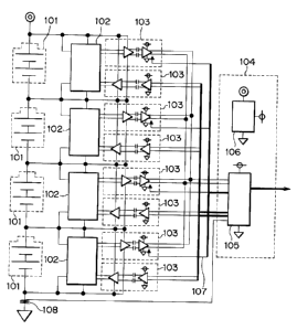
Fig. 1 shows a power storage device in a first
CA 02333805 2001-02-O1
8
embodiment according to the present invention. Shown in
Fig. 1 are storage battery units 101, battery circuits 102,
potential level changing circuits 103, a main circuit 104,
a microcomputer 105, a power supply 106, an enable signal
107 and a current measuring circuit 108. The four storage
battery units 101 are connected in series, and the battery
circuits 102 are connected in parallel to the storage
battery units 101, respectively. The battery circuits 102
are connected through the potential level changing circuits
103 to the main circuit 104.
Each battery circuit 102 has a voltage measuring
circuit and a bypass circuit, the battery circuit 102
measures voltage between the terminals of the corresponding
storage battery unit 101. The bypass circuit controls the
voltage of the corresponding storage battery unit to reduce
differences in voltage between the storage battery units
101 to the least possible extent.
The main circuit 104 has the microcomputer 105 and
the power supply 106. The output of the current measuring
circuit 108 is given to the microcomputer 105.
The microcomputer 105 estimates the open-circuit
voltages of the storage battery units 101, determines the
charged state of the storage battery units 101 and
difference in voltage between the storage battery units,
CA 02333805 2001-02-O1
9
displays remaining amount of charge, drives the bypass
circuits and controls the power storage device on the basis
of voltages between the terminals of the storage battery
units 101 and current measured by the current measuring
circuit 108.
Since the storage battery units 101 are connected in
series, each battery circuit 102 has a potential level
different from that of the main circuit 104. The potential
level changing circuits 103 change the different potentials
of the battery circuits 102 and provide electric signals.
In this embodiment, the potential level changing
circuits 103 are insulating couplers of a capacitive
coupling type. The potential level changing circuits 103
may be of other insulating coupling type, such as a
transformer coupling type or a photocoupler type, or may be
level shift circuits comprising MOS transistors and voltage
dividing resistors. Although an input to the insulating
couplers is a pair of differential signal to improve noise
withstand property, the same may be a single end. The
insulating couplers of this embodiment are capacitors, i.e.,
capacitive insulating barriers, interposed between the
battery circuits 102 and the main circuit 104.
An enable signal 107 is applied to each insulating
coupler. The outputs of the insulating couplers are given
CA 02333805 2001-02-O1
through a common point to the microcomputer 105. The
enable signal 107 controls the operations of the insulating
couplers. The outputs of the insulating couplers are
transferred through the common point to reduce the number
of inputs to the microcomputer 105. If the number of the
insulating couplers is small, the outputs of the insulting
couplers may be individually given to the microcomputer 105.
Thus, the battery circuits 102 respectively having
different potential levels and the main circuit 104 are
functionally connected to construct a power storage device
capable of monitoring and managing the individual storage
battery units and the series-connected storage battery
units. Since the circuits operate on the different
potential levels, respectively, the withstand voltages of
the circuits can be lowered to magnitudes large enough to
withstands the potential levels, respectively. Since the
main circuit 104 includes all the circuits that carry out
common functions including the determination of the charged
state of the storage battery units 101 and the voltage
differences between the storage battery units 101, the
number of circuits; the number of parts and power
consumption are reduced, and the power storage device can
be formed in a small size at a low cost.
Since control signals and measured values exchanged
CA 02333805 2001-02-O1
11
between the battery circuits 102 and the main circuit 104
are passed through the insulating couplers in pulse signals
of digital values in this embodiment, the deterioration of
control accuracy and the reduction of noise margin
accompanying signal transmission and potential change can
be prevented. Although Fig. 1 shows the series-connected
four storage battery units 101, naturally, the present
invention is applicable to a power storage device having
any number of series-connected storage battery units.
As apparent from the foregoing description, the
power storage device in the first embodiment has the small
number of circuits, is inexpensive and small, is capable of
operating at a low power consumption and in a high control
accuracy, has a high noise withstand capacity and is highly
reliable.
Second Embodiment
Fig. 2 shows a power storage device in a second
embodiment according to the present invention. Shown in
Fig. 2 are a selection circuit 121, a comparator 122, a
storage device 123, a corrective circuit 124 and voltage
measuring circuits 125.
Each of battery circuits 102 is provided with the
voltage measuring circuit 125 for measuring voltage
between the terminals of a storage battery unit 101. A
CA 02333805 2001-02-O1
12
main circuit 104 includes the selection circuit 121 and the
corrective circuit 124. The corrective circuit 124
includes a microcomputer 105, the comparator 122 and the
storage device 123. The selection circuit 121 selects the
output of each voltage measuring circuit 125 given thereto
through a potential level changing circuit 103 and gives
the same to the microcomputer 105 and the comparator 122.
The microcomputer 105 reads a correction reference V=ef,
i.e., a true value, from the storage device 123 and gives
the same to the comparator 122. The comparator 122
compares the output of the selection circuit 121 and the
correction reference Vref. The output signal of the
comparator 122 is given to the storage device 123.
A working voltage range is predetermined for the
storage battery units 101. A true value stored as a
correction reference in the storage device 123 is outside
the working voltage range.
The storage battery unit 101 is disconnected from
the voltage measuring circuit 125 and the correction
reference Vref of a reference power supply is applied to the
input of the voltage measuring circuit 125. Upon the
reception of the output of the selection circuit 121 in
this state, the microcomputer 105 decides that the power
storage device is in a correction mode. The comparator 122
CA 02333805 2001-02-O1
13
compares the voltage measured by the voltage measuring
circuit 125, i.e., the output of the selection circuit 121,
with the correction reference Vref and the difference
between the voltage measured by the voltage measuring
circuit 125 and the correction reference V=ef is stored as
an error in the voltage measuring circuit 125 in the
storage device 125 to complete the correction mode.
Then, the storage battery unit 101 is connected to
the voltage measuring circuit 125 to apply a working
voltage to the voltage measuring circuit 125 and the
microcomputer 105 executes a correction calculating process
on the basis of the stored error and a correction
expression. Thus, the error in the voltage measuring
circuit 125 is corrected to improve measuring accuracy and
reliability.
The correction reference Vref 1.S produced by reading
a value stored beforehand in the storage device 123 by the
microcomputer 105. A reference power supply may be used.
Although the correction circuit 124 includes the
microcomputer 105, the comparator 122 and the storage
device 123 in this embodiment, the comparator 122 and the
storage device 123 may be incorporated into the
microcomputer 105, which is effective in further reducing
power consumption, the number of parts and area necessary
CA 02333805 2001-02-O1
14
for laying out the component parts.
Third Embodiment
Fig. 3 shows a power storage device in a third
embodiment according to the present invention. Shown in
Fig. 3 are a correction switch 131 placed between the
output of a comparator 122 and the input of a storage
device 123. The correction switch 131 is opened during an
ordinary voltage measurement.
In the second embodiment, the microcomputer decides
whether or not the power storage device is in the
correction mode on the basis of the correction reference
Vref provided by the reference power supply applied to the
voltage measuring circuit 125. In the third embodiment,
when the correction switch 131 is closed, the comparator
122 is connected to the storage device 123, so that it is
possible to decide surely that the power storage device is
in the correction mode. Thus, an error in the correction
mode can be surely stored and reliability is improved.
Since this embodiment corrects a measured voltage after
potential change, errors that may be produced after
correction can be eliminated.
In this embodiment, the comparator 122 and the
storage device 123 may be incorporated into a microcomputer
105. In such a case, the microcomputer 105 is provided
CA 02333805 2001-02-O1
with a correction switch 131 or a signal input instead of
the correction switch 131. Thus, power consumption, the
number of parts and area necessary for laying out parts can
be reduced.
Fourth Embodiment
Fig. 4 shows a power storage device in a fourth
embodiment according to the present invention. Shown in
Fig. 4 are a correcting unit 141, a selection circuit 142
and a voltage measuring reference circuit 143.
The correcting unit 141 is provided with the
selection circuit 142, the voltage measuring reference
circuit 143 and a comparator 122. The input terminals of
the selection circuit 142 are connected to the terminals of
storage battery units 101. The output of the selection
circuit 142 is given through the voltage measurement
reference circuit 143 to the comparator 122. The voltage
measuring reference circuit 143 is a voltage measuring
circuit calibrated beforehand or having a guaranteed
accuracy and having an accurate redundant system.
In a correction mode, the comparator 122 compares
the output of a selected voltage measuring circuit 125 with
the reference output of the voltage measuring reference
circuit 143 and an error in the voltage measuring circuit
125 thus obtained is stored in a storage device 123.
CA 02333805 2001-02-O1
16
Subsequently, the microcomputer 105 processes
measured values measured by the voltage measuring circuits
125 to calculate corrections by using the stored errors and
a correction expression. Thus, errors in the voltage
measuring circuits 125 are corrected and measuring accuracy
and reliability are improved.
The power storage device may be provided with
voltage measuring reference circuits 143 for all the
storage battery units 101. However, since the voltage
measuring reference circuits 143 are comparatively
expensive and the provision of voltage measuring reference
circuits 143 for all the storage battery units 101
increases the number of parts, it is preferable to provide
the power storage device with the single voltage measuring
reference circuit 143 in combination with the selection
circuit 142 for all the storage battery units 101, as shown
in Fig. 4. The comparator 122 may be included in the
correcting unit 141. The correcting unit 141 may be
disconnected from the power storage device while the power
storage device is in a mode other than the correction mode.
Fifth Embodiment
Fig. 5 shows a power storage device in a fifth
embodiment according to the present invention. The fifth
embodiment is provided with insulating couplers that
CA 02333805 2001-02-O1
17
transmit differential transition signals instead of the
potential level changing circuits 103 shown in Figs. 1 to 4.
Shown in Fig. 5 are a differential amplifier circuit 201,
an insulating barrier 202, a load resistor 203, a
transition detecting circuit 204 and a pulse regenerating
circuit 205.
The first stage of the differential amplifier
circuit 201 is a CMOS differential amplifier. The
differential amplifier circuit 201 compares a reference
voltage Vref and an input pulse signal Pls_in and provides a
complementary signal Pls_10 indicating the results of
comparison. The second stage (driving stage) of the
differential amplifier circuit 201 is a CMOS inverter. The
CMOS inverter provides a complementary pulse signal pair
(output of the differential amplifier circuit) Pls_1 of an
amplitude approximately equal to a supply voltage.
The insulating barrier 202 is a capacitive
insulating barrier having a dielectric strength between the
primary and the secondary side. Diodes are connected in
reverse connection to between the respective terminals of
the primary and the secondary side and a high potential
power supply (VDD1 or VDD2) and a low potential power
supply (VSS1 or VSS2) to absorb surges due to noise or the
like.
CA 02333805 2001-02-O1
18
The load resistor 203 is a differential means for
giving an output of a differential waveform from the
terminal of the primary side to that of the secondary side
by capacitive coupling. The load resistor 203 is disposed
so as to short-circuit between the high potential power
supply VDD2 and the terminal of the secondary side.
Normally, the terminal of the secondary side is fixed at
the potential of the high potential power supply VDD2.
When the terminal of the primary side goes from HIGH to LOW,
a signal of a differential waveform spiked on the LOW side
is generated.
The transition detecting circuit 204 receives a
differential signal Pls_3, detects the leading edge and the
trailing edge of an input pulse signal Pls in and generates
a one-shot pulse signal Pls_4. The input stage of the
transition detecting circuit 204 is a pair of CMOS
differential amplifiers that receives the differential
signal pair Pls_3 in a reverse connection. The pair of
CMOS differential amplifiers provide single-end signals.
Since input signals to the CMOS differential amplifiers are
constantly on the same level, the load is a PMOS current
mirror.
Only when a potential difference is praduced between
the pair of differential signals Pls_3 (only when the input
CA 02333805 2001-02-O1
19
pulse signal Pls_in changed), the CMOS differential
amplifier provides a differential output (each CMOS
differential amplifier provides a single-end output) Pls-40
corresponding to the potential difference. In a steady
state, the respective levels of the outputs Pls_40 of the
pair of CMOS differential amplifiers are the same.
Therefore, the PMOS input level changing circuit is
designed so that PMOS input level changing circuit does not
provides an output signal of an intermediate level (a level
near the logical threshold of the next gate) when input
signals of the same level are applied thereto.
For example, a pulse regenerating (demodulating)
circuit 205 of the next stage including a flip-flop
receives signals by a CMOS NAND gate, the gate width of the
MOS gate of the level changing circuit is designed so that
the output of the pulse regenerating circuit 205 goes HIGH
when the levels of the Pls_40 are the same. Therefore, in
the level changing circuit that changes Pls_40 into Pls 4
shown in Fig. 5 the ratio between PMOS gate width and NMOS
gate width on the input side and the ratio between PMOS
gate width and NMOS gate width on the output side are
different from each other. In a steady state, both the
outputs of the transition detecting circuit 204 are HIGH,
and a one-shot pulse of LOW is generated on one side when
CA 02333805 2001-02-O1
the input pulse signal Pls_in rises and on the other side
when the input pulse signal Pls_in falls according to the
change of the input pulse signal Pls_in.
The pulse regenerating circuit 205 is a flip-flop
that regenerates the input pulse signal Pls_in and provides
an output pulse Pls_out on the secondary side when the
output signal Pls_4 of the transition detecting circuit 204
is applied thereto. In this embodiment, the pulse
regenerating circuit 205 is formed of a flip-flop including
two CMOS NAND gates, and a CMOS inverter driver. If
necessary, the pulse regenerating circuit 205 may be
provided with a resetting means for resetting the flip-flop.
In the insulating coupler of this embodiment, the
secondary terminal is short-circuited through the load
resistor 203 to the high-potential power supply VDD2.
Therefore, the rising operation of the primary side is
important. Therefore, when logical threshold VLT is lower
than (VDD - VSS)/2, the fall time is reduced and the CMOS
inverter of the output stage of the differential amplifier
circuit 201 is able to suppress the variation of timing.
In this embodiment, the circuits on the opposite
sides of the insulating barrier 202 are differential
circuits. Therefore, property to withstand common mode
noise is improved and S/N ratio increases. The transition
CA 02333805 2001-02-O1
21
detecting circuit 204 connected to the output of the
insulating barrier 202 consists of a pair of differential
amplifiers. Therefore, an amplifier excellent in CMRR
(common mode rejection rate) can be formed. Since the
insulating coupling circuit is formed of simple CMOS gates,
the power storage device is capable of dealing with low
voltages of 5 V or below (to a low volt on the order of 1.8
V) and hence power consumption is small.
Fig. 6 is a timing chart of assistance in explaining
the operation of the circuit shown in Fig. 5. Upon the
reception of the input pulse signal Pls_in, the
differential amplifier circuit 201 provides the
differential signal Pls_1. The load resistor 203 coupled
by capacitive coupling with the primary side of the
insulating barrier 202 provides the differential signal
Pls_3. The output signal Pls_4, i.e., the transition
detection signal Pls_4, of the transition detecting circuit
204 is a rectangular pulse signal synchronous with the
differential signal Pls_3. The pulse regenerating circuit
205, i.e., the last output stage, provides the regenerated
pulse signal Pls out identical with the input signal Pls_in.
The regenerated pulse signal Pls_out is a rectangular pulse
signal complementary to and synchronous with the transition
detection signal Pls_4. Thus, the differential insulating
CA 02333805 2001-02-O1
22
coupler provides the transition signal of a differential
waveform, which reduces the power consumption of the
insulating coupler.
Sixth Embodiment
Fig. 7 shows a power storage device in a sixth
embodiment according to the present invention. Shown in
Fig. 7 are active filters 401 and voltage measuring
circuits 402. The power storage device in the sixth
embodiment is the same as those in the first to the six
embodiment, except that each of battery circuits 102
includes the active filter 401 in the sixth embodiment.
Each active filter 401 includes OP amplifiers, resistors
and a capacitor. Each active filter 401 is interposed
between the voltage measuring circuit 402 and a storage
battery unit 101.
The active filter 401 eliminates noise components
superposed between the terminals of the storage battery
units 101 and gives the do voltage components of the
storage battery unit 101 to the voltage measuring circuit
402. Thus, the erroneous voltage measurement of the
voltage measuring circuit 402 due to the influence of the
noise components can be prevented, and accuracy and
measurement of voltage measurement are improved.
Seventh Embodiment
CA 02333805 2001-02-O1
23
Fig. 8 shows a power storage device in a seventh
embodiment according to the present invention. Shown in
Fig. 8 are voltage-time conversion circuits 501, charging
switches 502, capacitors 503, discharging switches 504,
decision circuits 505, a time-voltage conversion circuit
506 and charge-and-discharge resistors 507.
The voltage-time conversion circuit 501 is included
in a battery circuit 102 and comprises the charging switch
502, the discharging switch 504 connected in series to the
charging switch 502, the capacitor 503 connected through
the charge-and-discharge resistor 507 in parallel to the
discharging switch 504, and the decision circuit 505 having
an input connected to the common joint of the charge-and-
discharge resistor 507 and the capacitor 503. The time-
voltage conversion circuit 506 has a comparator. An
insulating coupler 103 connecting the voltage-time
conversion circuits 501 and the time-voltage conversion
circuit 506 is a single end, has insulating barriers 202
having secondary sides connected together, and the joint of
the secondary sides of the insulating barriers 202 is
connected to a load resistor 203, a transition detecting
circuit 204 and a pulse regenerating circuit 205.
The operation of the voltage-time conversion circuit
501 will be described. The charging switch 502 is closed
CA 02333805 2001-02-O1
24
and the discharging switch 504 is opened to charge the
capacitor 503 to a voltage equal to the terminal voltage V$
of the storage battery unit 101. Then, the charging switch
502 is opened and the discharging switch 504 is closed to
discharge the capacitor 503. The output of the decision
circuit 505 is inverted upon the drop of the voltage of the
capacitor 503 to a threshold voltage VTH (the gate threshold
voltage of A MOSFET included in the decision circuit 505 in
this embodiment).
The threshold voltage VTH and discharge time t is
expressed by:
VTH = V~ ' exp ( - t / CR ) . . . . . . . . . . ( 1 )
t = C~R~ln(V~/VTx) .......... (2)
where t is the discharge time of the capacitor 503, V~ (=VB)
is the voltage of the capacitor 503, C is the capacitance
of the capacitor 503, and R is the resistance of the
charge-and-discharge resistor 507.
The voltage-time conversion circuit 501 converts the
voltage V$ (= V~) of the storage battery unit 101 into the
discharge time t, i.e., the pulse width or the pulse
interval of the output of the decision circuit 505.
Charging time, similarly to the discharge time t, is
converted into pulse width or pulse interval. As obvious
CA 02333805 2001-02-O1
from Expression (2), the conversion accuracy of the
voltage-time conversion circuit 501 is dependent on C, R
and VTH. Therefore, devices having characteristics varying
in narrow ranges are employed as the capacitor 503, the
discharging switch 504, the charge-and-discharge resistor
507 and the decision circuit 505. In particular, it is
preferable to employ a bipolar transistor having
characteristics varying in a narrow range or a precision
comparator for the decision circuit 505. A bipolar
transistor has a built-in potential stable under variable
temperature and is preferable to reduce the variation of
the threshold voltage VTH. Generally, capacitance C and
resistance R vary with temperature. Therefore, when
necessary, a value calculated by using Expression (2) is
corrected for temperature correction.
The time-voltage conversion circuit 506 compares the
output of the pulse regenerating circuit 205 and a clock
signal (CLK signal) by the comparator and generates a pulse
train in a period when the output of the pulse regenerating
circuit 205 is HIGH. The microcomputer 105 counts the
number of pulses of the pulse train and converts the output
of the pulse regenerating circuit 205 into a voltage
corresponding to the number of pulses. If the voltage of
the capacitor 503 is 5 V, the capacitor 503 is discharged
CA 02333805 2001-02-O1
26
for 1 ms and the frequency of the CLK signal is 16 MHz.
Then,
1 ms/(1/16 MHz) - 16,000 pulses ...... (3)
and therefore,
V/16000 = 0.33 mV ...._. (4)
Thus, this embodiment is capable of achieving
voltage measurement in a high measuring accuracy.
A microcomputer having an input capture function may
be used instead of the comparator of the time-voltage
conversion circuit 506.
In this embodiment, the secondary sides of the
insulating barriers 202 of the insulating coupler are
connected together and the joint of the secondary sides of
the insulating barriers 202 is connected to the load
resistor 203, the transition detecting circuit 204 and the
pulse regenerating circuit 205. Therefore, the voltage-
time conversion circuits 501 respectively connected to the
storage battery units 101 operates sequentially.
In this embodiment, the microcomputer 105 measures
the voltages of the storage battery units 101. If the
voltages of the storage battery units 101 are different
from each other, the microcomputer 105 closes the charging
switch 502 and the discharging switch 504 of the voltage-
time conversion circuit 501 connected to the storage
CA 02333805 2001-02-O1
27
battery unit 101 of a voltage higher than that of the other
storage battery unit 101 simultaneously. Consequently, the
bypassing or self-discharging of charging current is
carried out through the series circuit of the charging
switch 502 and the discharging switch 504 to eliminate the
voltage difference.
In this embodiment, the charge-and-discharge
resistor 507 not included in the series circuit of the
charging switch 502 and the discharging switch 504 is
interposed between the discharging switch 504 and the
capacitor 503 to adjust discharge time. Therefore,
discharge time can be adjusted by properly determining the
resistance of the charge-and-discharge resistor 507 so that
voltage can be measured in a satisfactory accuracy even if
the resistances of the switches are reduced to increase
bypass current. Thus, this embodiment uses the voltage
measuring circuit and the bypass current for both the
series-connected storage battery units 101 to achieve both
voltage measurement and voltage difference elimination.
Fig. 9 is a timing chart of assistance in explaining
the operation of the power storage device shown in Fig. 8.
The capacitor 503 is charged to a voltage equal to that of
the storage battery unit 101 in a period where the charging
switch 502 is closed (HIGH). When the charging switch 502
CA 02333805 2001-02-O1
28
is opened (LOW) and the discharging switch 504 is closed,
the voltage of the capacitor 503 decreases at an
exponential rate. Upon the decrease of the voltage of the
capacitor 503 below a predetermined voltage, the output of
the decision circuit 505 (transition detecting circuit 205)
goes LOW. The comparator compares the output of the
transition detecting circuit 205 with a clock signal CLK
and generates a pulse train until the output of the
decision circuit 505 (transition detecting circuit 205)
goes LOW.
The microcomputer 105 counts the number of pulses of
the pulse train while the discharging switch 504 is closed
and converts the number of pulses into a corresponding
voltage. If the number of pulses of the pulse train is
less than a predetermined number, it is decided that the
storage battery unit 101 is overdischarged or that the
charging switch 502 is malfunctioning. If the number of
pulses of the pulse train is a predetermined number or more,
it is decided that the storage battery unit 101 is
overcharged or that the discharging switch 504 is
malfunctioning. If any pulse train is not generated while
the charging switch 502 is closed, it is decided that the
storage battery unit 101 is overdischarged, that the
storage battery unit 101 is short-circuited or the charging
CA 02333805 2001-02-O1
29
switch 502 is malfunctioning.
When the charging switch 502 and the discharging
switch 504 of the voltage-time conversion circuit 501 are
used as a bypass circuit, the condition of a balancing
circuit, i.e., whether a balancing circuit is normally
operating, can be verified through the decision of whether
any pulse train is generated.
Thus, this embodiment has abilities to detect the
state of the storage battery unit 101, such as an
overcharged state, an overdischarged state or a short-
circuited state, and to verify the operation of the
voltage-time conversion circuit 501 serving also as a
bypass circuit in addition to abilities to measure voltage
and potential difference elimination. Since the bypass
circuit has the charging switch 502 and the discharging
switch 504 which are connected in series, the bypass
circuit can be surely disconnected by one of the switches
502 and 504 even if the other switch is short-circuited.
Eighth Embodiment
Fig. 10 shows a power storage device in an eighth
embodiment according to the present invention. Shown in
Fig. 10 are a corrective reference circuit 701, a switch
702 and a reference power supply 703, such as a Zener diode.
The corrective reference circuit 701 has the switch 702 and
CA 02333805 2001-02-O1
the reference power supply 703.
When necessary, a charging switch 502 and the switch
702 are closed to charge a capacitor 503 to a voltage equal
to that of the reference power supply 703. Then, the
charging switch 502 and the switch 702 are opened, and a
discharging switch 504 is closed to discharge the capacitor
503.
Since the reference voltage Vref of the reference
power supply 703 is known, an error in discharge time t
with respect to reference discharge time tref due to the
influence of the capacitance C of the capacitor 503, the
resistance R of the discharging switch 504, the threshold
voltage VTH of a decision circuit and temperature T on time-
voltage conversion is corrected.
When the voltage of the reference power supply 703
is Vref, and discharge time therefor is trefl, the following
expression is expressed.
Vrefl = VTH'exp(trefl~C~R) . . . . . . . . .. (5)
From Expression (5), time t necessary for discharging the
capacitor 503 charged at V~ is expressed by:
t = C~R~ln(V~~V=efl) + trefl ..........
Thus, the threshold voltage VTH can be determined from the
discharge time t. Expression (6) can be rewritten as
follows when the power storage device is provided
CA 02333805 2001-02-O1
31
additionally with a second reference power supply, not
shown, the voltage is Vref2 and discharge time is tref2
t = ( tref2 - trefl ) ~ In ( Vc~Vrefl ) ~~-n ( Vref2~Vref1 ) '~' trefl
.......... (7)
Therefore, the voltage V~ of the storage battery unit 101
can be determined on the basis of the discharge time t even
if C and R are unknown. Thus, the voltage V~ of the storage
battery unit 101 can be accurately determined even if the
capacitance C of the capacitor 503 and the resistance R of
the discharging switch 504 are unknown. As obvious from
Expression (7), the time t is independent of the
capacitance C and the resistance R, and hence the voltage
V~ of the storage battery unit 101 can be accurately
determined even if the capacitance C and the resistance R
change due to temperature change.
Ninth Embodiment
Fig. 11 shows a power storage device in a ninth
embodiment according to the present invention. Shown in
Fig. 11 are storage batteries 801 and a level shifting
circuit 802. The level shifting circuit 802 includes PMOSs
and resistors RH and RL. The level shifting circuit 802
changes the potential level and the amplitude of an input
signal in the ratio between the resistances of the
resistors RH and RL. In this embodiment, a storage battery
CA 02333805 2001-02-O1
32
unit 101 is formed by connecting the plurality of storage
batteries 801 in series. A battery circuit 102 includes
voltage-time conversion circuits 501 respectively connected
to the storage batteries 801, correction reference circuits
701, the level shifting circuit 802, and a time-voltage
conversion circuit 506. As shown in Fig. 11, the outputs
of the voltage-time conversion circuits 501 are connected
to the resistor RL of the level shifting circuit 802.
In this embodiment, the storage batteries 801 are
lithium secondary batteries having a maximum supply voltage
of 4.2 V. Therefore, the maximum supply voltage of the
storage battery unit 101 is 16.8 V when the number of the
storage batteries 801 is four and is 33.6 V when the number
of the storage batteries 801 is eight. Therefore, the
battery circuit 102 may comprise general semiconductor
devices having a rated voltage of 18 V or 36 V. When the
number of the series-connected storage batteries 801 is
eight or below, the battery circuits 102 can be easily
embodied by IC chips of the same type or hybrid ICs of the
same type, so that the number of parts can be reduced, and
the power storage device can be formed in a small size at
low costs.
Tenth Embodiment
Fig. 12 shows a tenth embodiment according to the
CA 02333805 2001-02-O1
33
present invention in a plan view. Shown in Fig. 12 are a
SOI (silicon-on-insulator) wafer 901, isolation trenches
902 and bonding pads 903. The isolation trenches 902 are
formed by filling up trenches formed in the SOI wafer 901
with an insulating material. Battery circuits 102,
insulating couplers 103 and a main circuit 104 formed on
the SOI wafer 901 are surrounded by the isolation trenches
902, respectively, and are integrated on the SOI wafer 901.
Fig. 13 is a sectional view of the tenth embodiment
shown in Fig. 12. Shown in Fig. 12 are an insulating layer
1001, a semiconductor layer 1002 and a protective layer
1003. The semiconductor layer 1002 is divided by the
isolation trenches 902 into from the left toward the right
as viewed in Fig. 12, and a battery circuit region for a
battery circuit 102, a potential level changing circuit
region for a potential level changing circuit 103 and a
main circuit region for a main circuit 104 are disposed.
The structure shown in Fig. 12, the SOI wafer 901 has the
about 2 Eun thick insulating layer 1001 of Si02 , and the
regions are formed are formed by thin-film deposition
processes using photomasks.
The SOI wafer 901 is formed by forming the
insulating layer 1001 formed of a single Si02 film or of a
multilayer polysilicon film formed by superposing
CA 02333805 2001-02-O1
34
polysilicon films each having an oxidized surface, and
forming a semiconductor layer of single-crystal silicon on
a single-crystal silicon substrate. In this embodiment,
the polysilicon films are bonded together by mirror-
finishing the silicon dioxide layers on the polysilicon
films, superposing the polysilicon films and subjecting the
superposed polysilicon films to a heat treatment that heats
the superposed polysilicon films at a specific temperature
to form the multilayer polysilicon layer.
The isolation trenches 902 are insulating Si02 layers.
The isolation trenches 902 are formed by a method that
forms trenches and fills up the trenches with Si02 or BPSG
(borophosphosilicate glass), a method that forms trenches,
oxidizes the surfaces of the trenches in a small depth and
fills up the trenches with polysilicon, a method that
applies a PIV (polyimide varnish) or SOG (spin-on-glass) or
a method that bombards the surface of the semiconductor
layer with oxygen ions to convert the semiconductor layer
into an insulating layer.
The protective layer 1003 is an insulating film of
Si02, an HLD film (high-temperature low-pressure
decomposition film) or an SiN film. Wiring layers of
polysilicon and those of aluminum are covered with the
protective layer 1003.
CA 02333805 2001-02-O1
The insulting barrier 202 of the insulating coupler
includes three electrode regions 202a, 202b and 202c and
the insulating trenches 902. Dielectric strength can be
secured by connecting the insulating barriers 202 in series
even in the trench system in which the width of the
insulating trenches 902, as compared with the thickness of
the insulating layer 1001, is limited.
When the insulating barrier 202 is formed in a
pattern resembling a folded band to increase the length of
parts in contact with the electrode regions, a necessary
capacitance can be obtained even if the area of the
semiconductor is small. In this embodiment, the
capacitance of an area about 160 wm square is about 2 pF,
and one insulating trench 902 has a dielectric strength of
about 750 V measured by a withstand voltage test. The
insulating trenches 902 are formed in a pattern having
folded parts and corners rounded as far as possible in
circular arcs of radii of curvature in the range of 2 to 5
Eun to maintain dielectric strength.
In this embodiment, a plurality of circuits are
isolated from the substrate 901 by the insulating trenches
902 and the insulating layer 1001. Therefore, this
integrated circuit can be directly bonded to a frame in
packaging the integrated circuit and hence heat can be
CA 02333805 2001-02-O1
36
efficiently dissipated. In this embodiment, the insulating
layer is formed of a plurality of layers and the respective
thicknesses of the layers are formed in proper thicknesses,
so that stress is distributed uniformly to reduce the warp
of the substrate.
When this embodiment has a battery unit 101 of a
lithium secondary battery, the maximum supply voltage of
the battery unit 101 is on the order of 4.2 V. Therefore,
the withstand voltages of the battery circuit 102 and the
main circuit 104 may be on the order of 5 V; that is, the
withstand voltages of the circuits surrounded by the
insulating trenches 902 may be on the order of 5 V.
When the battery unit 101 of this embodiment is
formed by connecting 96 lithium secondary batteries in
series, the maximum supply voltage of the battery unit 101
is about 400 V, which is far lower than the withstand
voltage of the insulating trenches 902. Therefore, the
insulating couplers and the other circuits can be formed on
the SOI wafer 901 in an integrated circuit. Thus, a small,
reliable, inexpensive power storage device having a small
number of circuits, capable operating at a low power
consumption, excellent in control accuracy and having high
noise margin can be obtained.
Eleventh Embodiment
CA 02333805 2001-02-O1
37
Fig. 14 shows an eleventh embodiment of the present
invention. The eleventh embodiment has a battery circuit
102 similar to that of the ninth embodiment and formed on a
silicon wafer 1101. As shown in Fig. 14, a monolithic IC
has the silicon wafer 1101 and components formed on the
silicon wafer 1101. The components include voltage-time
converting circuits 501, correction reference circuits 701
and level shifting circuits 506.
In this embodiment, the storage batteries 801 of a
storage battery unit 101 are lithium secondary batteries
having a maximum supply voltage of 4.2 V. Therefore, the
maximum supply voltage of the storage battery unit 101 is
16.8 V when the number of the storage batteries 801
connected in series is four and is 33.6 V when the number
of the storage batteries 801 connected in series is eight.
Therefore, the withstand voltages of the battery circuit
102 and the level shifting circuits 802 may be 18V or 36 V
and hence the components can be easily formed on the same
silicon wafer in a monolithic IC. This embodiment reduces
the number of parts, and forms a small, inexpensive power
storage device.
Twelfth Embodiment
Fig. 15 shows a twelfth embodiment of the present
invention. Shown in Fig. 15 are a commercial power source
CA 02333805 2001-02-O1
38
1201, a solar power generating system 1202, load devices
1203, a control converter 1204, switches 1205 and a
multiplexer 1206. A plurality of storage battery units 101
are connected in series, and battery circuits 102 are
connected across the opposite ends of the storage battery
units 101, respectively. The output of each battery
circuit 102 is connected through an insulating coupler and
the multiplxer 1206 to a main circuit 104. The control
converter 1204 is connected across the opposite ends of the
series circuit of the storage battery units 101. A
microcomputer 105 included in the main circuit 104, and an
MCU (microprocessor control unit) included in the control
converter 1204 are connected through an insulating coupler.
The solar power generating system 1202, the load
devices 1203 and the control converter 1204 are connected
through the switches 1205 to the commercial power source
1201. The solar power generating system 1202, the load
devices 1203, the control converter 1204, the switches 1205
and the main circuit 104 are connected bilaterally by
insulating couplers 103.
The solar power generating system 1202 converts
solar energy into do power by solar cells, and converts the
do power into ac power by an inverter. The load devices
1203 are domestic electric appliances including air
CA 02333805 2001-02-O1
39
conditioners, refrigerators, electronic ovens and
illuminating devices, and electric apparatuses including
motors, computers and medical appliances. The control
converter 1204 is a charge-and-discharge device that
converts ac power into do power or coverts do power into ac
power. The control converter 1204 controls the solar power
generating system 1202 and the load devices 1203 in
addition to charging and discharging operations.
Those devices are connected to the switches 1205. A
power storage device in this embodiment may be connected to
control converters 1204 other than that shown in Fig. 15
and other devices.
When power demand of the load devices 1203 shown in
Fig. 15 cannot be met by the commercial power source 1201
and the solar power generating system 1202, power is
supplied from the storage battery units 101 through the
control converter 1204. When excessive power is supplied
by the commercial power source 1201 and the solar power
generating system 1202, the control converter 1204 uses the
surplus power for charging the storage battery units 101.
When the supply voltages of the storage battery
units 101 rise to discharge stopping level or a charge
stopping level during the foregoing operations, the main
circuit 104 gives a signal to that effect to the control
CA 02333805 2001-02-O1
converter 1204 and then the control converter 1204 controls
discharging or charging.
This embodiment enables the reduction of contract
demand and consumption of power supplied by the commercial
power source 1201, and the rated output power of the solar
power generating system 1202, which reduces equipment cost
and running cost.
The storage battery units 101 supply power to the
commercial power source 1201 in a specific time band where
power demand very high, and surplus power is stored in the
power storage system while power demand is low. Thus, the
concentration of power demand on the commercial power
source 1201 can be moderated and power supply of the
commercial power source 1201 can be leveled off.
The control converter 1204 monitors the power
consumption of the load devices 1203 and controls the load
devices 1203 to save energy and to use power effectively.
Fig. 16 is a graph of assistance in explaining
operations of this embodiment for processing measured data,
in which voltage V is measured on the vertical axis (Y-
axis) and a current is measured on the horizontal axis (X-
axis).
The relation between measured voltage data measured
by a voltage measuring circuit 125 and stored in a certain
CA 02333805 2001-02-O1
41
period and measured current data measured by a current
measuring circuit 108 in the same period was approximated
by an approximate straight line determined by a least-
squares method.
The Y-intercept, i.e., a value of voltage
corresponding to X = 0, is the open-circuit voltage OCV of
the storage battery unit 101. The gradient of the
approximate straight line corresponds to the internal
resistance R of the storage battery unit 101. The
approximate straight line is expressed by: Y = R~I + OCV.
A microcomputer processes measured voltage data measured by
the voltage measuring circuit 125 and the measured current
data measured by the current measuring circuit 108 to
determine the open-circuit voltage and the internal
resistance of the storage battery unit 101. The
microcomputer estimates the residual capacity and the life
of the storage battery unit 101 on the basis of the
measured data.
Thirteenth Embodiment
Fig. 17 shows a thirteenth embodiment of the present
invention. Fig. 17 shows an essential part of an algorithm
to be carried out by the microcomputer included in the
circuit shown in Fig. 15.
In Fig. 15, the microcomputer 105 of the main
CA 02333805 2001-02-O1
42
circuit 104 and the MCU of the control converter 1204 are
associated with the power storage device. The MCU and the
microcomputer 105 are connected by communication lines.
Each battery circuit 102 includes a voltage-time conversion
circuit 501 that serves also as a voltage measuring circuit
125. The output of the battery circuit 102 is applied
through the potential level changing circuit 103 and the
multiplexer 1206 to the input capture terminal, not shown,
of the microcomputer 105. The output of the current
measuring circuit 108 is applied to the MCU.
In the battery circuits 102 and the main circuit 104,
all charging switches 502 are closed. When measurement
start command is provided in the current measuring circuit
108 and the MCU, the measurement start command is sent out.
During communication, a reception completion interrupt and
a transmission completion interrupt occur on the sending
and the receiving side substantially simultaneously. Then,
the battery circuits 102 and the main circuit 104 opens all
the charging switches 502. The current measuring circuit
108 and the MCU start current measurement.
Operations for current measurement and opening the
plurality of charging switches 502 are carried out
substantially simultaneously; that is, the voltage clamping
and current measurement of the plurality of storage battery
CA 02333805 2001-02-O1
43
units 101 are carried out simultaneously.
Since the output of the voltage-time conversion
circuit 501 is applied through the multiplexes 106 to the
input capture terminal as shown in Fig. 15, only one of the
discharging switches a504 is closed on the side of the
battery circuits 102 and the main circuit 104 and then
operations for time-voltage conversion and voltage
recording are carried out. Then, the next discharging
switch b is closed and the same operations are repeated.
In this case, since the voltage at the measurement
of current has been clamped, the simultaneity of the
measured voltage data and the measured current data can be
achieved even through operations for the time~voltage
conversion of the plurality of storage battery units 101
are carried out sequentially.
Fourteenth Embodiment
Fig. 18 is a typical view of a fourteenth embodiment
of the present invention. Shown in Fig. 18 are a personal
computer 1207, a card slot 1208, a PC card 1209, a current
probe 1210 of a storage battery unit 101, and voltage
probes 1211 for measuring the supply voltages of the
storage battery units 101. The PC card 1209 is provided
with battery circuits 102, potential level changing
circuits 103 and a main circuit 104. The PC card 1209 is
CA 02333805 2001-02-O1
44
inserted in the card slot 1208 of the personal computer
1207. The current probe 1210 and the voltage probes 1211
are connected to the PC card 1209.
This embodiment is an evaluation device using the
current probe 1210 and the voltage probes 1211 as measuring
terminals. In particular, when the potential level
changing circuits 103 include insulating couplers, the
supply voltages of the storage battery units 101 can be
measured even if the potential level of the personal
computer 1207 is different from that of the current probe
1210 and the voltage probes 1211.