Note: Descriptions are shown in the official language in which they were submitted.
CA 02334156 2001-11-19
-1-
RADIO FREQUENCY IDENTIFICATION TAG HAVING AN ARTICLE
INTEGRATED ANTENNA
Field of the Invention
The present invention relates generally to the field of radio-
frequency identification tags including, but not limited to, radio frequency
identification tags having an article integrated antenna.
Background of the Invention
Radio frequency identification (RFID) tags and radio frequency
identification tag systems are known, and find numerous uses. For
example, radio frequency identification tags are frequently used for
CA 02334156 2000-12-04
WO 99/65002 PCT/US99/12640
_2_
personal identification in automated gate sentry applications protecting
secured buildings or areas. Information stored on the radio frequency
identification tag idenitifies the person seeking access to the secured
building. A radio frequency identification tag system conveniently
5 provides for reading tlhe information from the radio frequency
identification
tag at a small distance using radio frequency (RF) data transmission
technology. Most typically, the user simply holds or places the radio
frequency identification tag near a base station that transmits an excitation
signal to the radio frequency identification tag powering circuitry contained
on the radio frequency identification tag. The circuitry, responsive to the
excitation signal, communicates the stored information from the radio
frequency identification tag to the base station, which receives and
decodes the information. In general, radio frequency identification tags
are capable of retaining and, in operation, transmitting a substantial
amount of information - sufficient information to uniquely identify
individuals, packages, inventory and the like.
A typical technology for powering and reading a radio frequency
identification tag is inductive coupling or a combination of inductive power
coupling and capacitive data coupling. Inductive coupling utilizes a coil
20 element in the radio frequency identification tag. The coil element is
excited (or "energized") by an excitation signal from the base station to
provide power to the radio frequency identification tag circuitry. The radio
frequency identification tag coil, or a second tag coil, may be used to
transmit and receive l:he stored information between the radio frequency
25 identification tag and the base station. Radio frequency identificatian
tags
relying on inductive coupling are sensitive to orientation of the radio
frequency identification tag with respect to the base station since the field
created by the excitation signal must intersect the coil element at
substantially a right angle for effective coupling. Read ranges for
30 inductively coupled devices are generally on the order of several
centimeters. Longer read distances are desirable, and for certain
applications, such as electronic animal identification, baggage tracking,
parcel tracking and inventory management applications, are necessary.
Another technology for powering and reading radio frequency
35 identification tags is electrostatic coupling such as employed in the radio
CA 02334156 2000-12-04
WO 99/65002 PCT/US99/12640
-3-
frequency identificatioin tag systems and radio frequency identification
tags disclosed in the above referenced applications. These systems
advantageously provide for substantially increased read/write distances
over those available in the prior art. Another advantage derived from the
use of the systems arnd tags therein disclosed is that the user need not
bring the radio frequency identification tag in close proximity to a base
station or to substantially orient the tag with respect to the base station.
It
is therefore possible to incorporate the antenna elements of the base
station into, for example, a doorway or a vestibule, a package conveyer or
an article sorting system, and to energize the tag and read the tag
information at a greater distance.
To couple either the inductive or electrostatic signals between the
base station and the radio frequency identification tag, the tag necessarily
includes an antenna having at least one and frequently two antenna
elements. Typically, a tag circuit chip and the antenna are electrically
coupled and bonded to a tag substrate. The tag dimensions, governed by
the tag substrate dimensions, are typically maintained fairly small.
Therefore, the antenna is generally size limited. A smaller antenna,
however, adversely afl~ects read ranges. Also, the antenna is necessarily
formed co-planar with the tag substrate potentially making the tag
orientation sensitive. l3ecause it is undesirable and generally impractical
to make the radio frequency identification tag larger, effective antenna
size remains limited. And, the typical flat tag design also limits the
antenna to a flat, orientation sensitive configuration.
To date radio frequency identification tags have been
manufactured as self-contained units, i.e., tag circuit chip, antenna and
substrate as a singular package. Therefore, not only has the size and
configuration of the antenna posed problems with performance of the
radio frequency identification tag, the antenna contributes significantly to
the cost of a completed tag.
Applications for radio frequency identification tags include personal
identification badges, article andlor package identification tags, and
electronic article surveillance tags. In many of these applications, the
identification badge, the article and/or package is substantially larger than
the radio frequency idE;ntification tag used to provide the identifying
CA 02334156 2000-12-04
WO 99/b5002 PCT/US99/12640
-4-
information. However, the size of the identification badge, article or
package has not offered an opportunity for increasing the size or reducing
the orientation sensitivity of the antenna of a self contained radio
frequency identification tag.
Thus, there is a~ need for an improved radio frequency identification
tag.
Brief Description of the Drawings
Preferred exemplary embodiments of the invention are illustrated in
the accompanying drawings in which like reference numerals represent
like parts throughout.
FIG. 1 is an exploded assembly view of a radio frequency
identification tag in accordance with a preferred embodiment of the
present invention.
FIG. 2 is a cross-section view taken along line 2-2 of FIG. 1.
FIG. 3 is a perspective view of a radio frequency identification tag
circuit chip assembly partially broken away to reveal a conductor element
formed therein.
FIG. 4 is a cross-section view taken along line 4-4 of FIG. 3.
FIG. 5 is an exploded assembly view of a radio frequency
identification tag in accordance with a preferred embodiment of the
present invention.
FIG. 6 is a cross-section view taken along line 6-6 of FIG. 5.
FIG. 7 is a perspective view of a radio frequency identification tag
circuit chip assembly.
FIG. 8 is a cross-section view taken along line 8-8 of FIG. 7.
FIG. 9 is an exploded assembly view of a radio frequency
identification tag in accordance with an alternate preferred embodiment of
the present invention.
FIG. 10 is a cross-section view taken along line 10-10 of FIG.. 9.
FIG. 11 is a crass-section view similar to the view of FIG. 10 and
illustrating an alternate preferred embodiment of the present invention.
FiG. 12 is a cross-section view of a radio frequency identification
tag in accordance with an alternate preferred embodiment of the present
invention.
CA 02334156 2000-12-04
WO 99/65002 PCT/US99/12640
-5-
FIG. 13 is a cross-section view of a radio frequency identification
tag in accordance with an alternate preferred embodiment of the present
invention.
FIG. 14 is a cross-section view of a radio frequency identification
tag in accordance with an alternate preferred embodiment of the present
invention.
FIG. 15 is a perspective view of an unassembled package
container in accordance with a preferred embodiment of the present
invention.
10 FIG. 16 is a perspective view of an assembled package container
in accordance with a preferred embodiment of the present invention.
Detailed Description of the Preferred Embodiments
Radio frequency identification tags in accordance with preferred
embodiments of the present invention utilize an antenna formed in
association with, and thus integral to, an article, package, package
container, label and/or identification badge ("article"). In a preferred
embodiment of the present invention, a radio frequency identification tag
circuit chip assembly is secured to the article and is electrically coupled to
the antenna formed o~n the article. Printing a conductive pattern on the
article using conductive ink forms a preferred antenna.
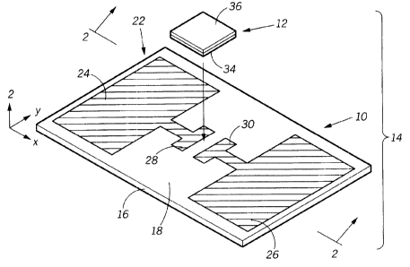
Referring to FIG. 1 of the drawings, shown in exploded assembly
view radio frequency identification tag 14 includes an article 10 and a
radio frequency identiification tag circuit chip assembly ("chip assembly")
25 12. Article 10 is shown generally as a substrate 16 formed from a sheet
of material having a first surface 18 and a second surface 20. It will be
appreciated that substrate 16 may form the basis for a personal
identification badge, a label, a package container (such as a box or
envelope) and the like. Moreover, the substrate material may be any
30 suitable material for the particular application such as plastic (including
polyester and metalized polyester material), paper, synthetic paper,
reinforced paper, cardboard, synthetic paper coated cardboard and the
like. As will be described with respect to alternate preferred embodiments
of the invention belo~nr, a radio frequency identification tag circuit chip
may
35 be attached directly to a substrate arranged with an integrally formed
CA 02334156 2000-12-04
WO 99/65002 PCT/U599/12640
-6-
antenna. The arrangement of chip assembly 12 advantageously provides
manufacturing convenience since many chip assemblies may be
produced in high volume using automated techniques. The chip
assemblies 12 are relatively small, on the order of 1 - 2 cm square, and
thus easier to store, slhip and handle versus the article to which it is
attached. Moreover, chip assembly 12, as will be described, provides for
a substantially simplified way of attaching the radio frequency
identification tag circuit chip to an article, and concomitantly coupling the
same to the integrally formed antenna.
Formed on first surface 18 is an antenna 22 including a first
antenna element 24 and a second antenna element 26. Each of first
antenna element 24 and second antenna element 26 are a formed from a
conductive material that is bonded or otherwise secured to, and thus
integral to, article 10. Most preferably, each of first antenna element 24
and second antenna element 26 are formed by printing, using a suitable
printable conductive medium. For example, a carbon/graphite based
conductive ink forms an effective antenna 22 when printed onto paper
and/or cardboard. Synthetic and coated papers may alternatively be
used, but at added cost. Silver and other precious metal inks may be
used particularly for pirinting on plastic materials, but are less preferred
due to higher material costs. Antenna 22 is shown to have a generally
broken "H" shape as vvould be suitable for use in an electrostatic signal
application. It will be .appreciate that other patterns more suitable to, for
example, inductive coupling may be printed without departing from the fair
scope of the present invention. Each of first antenna element 24 and
second antenna element 26 include at generally the center of the broken
"H" pattern, respectively, a first coupling region 28 and a second coupling
region 30. Most preferably, antenna 22 may be made substantially larger
than in traditional radio frequency identification tag construction,
approaching the surface area of surface 18. Each of first coupling region
28 and second coupling region 30 includes a conductive pad area for
electrically coupling to chip assembly 12 by means of a layer 34 of
anisotropic adhesive (FIG. 2).
A preferred anisotropic adhesive is 3M 9703 adhesive available
from 3M Corporation. The preferred adhesive is anisotropic in that it
CA 02334156 2000-12-04
WO 99165002 PCT/US99/12640
-7-
conducts in the "z" or vertical direction only (FIG. 1 ). The adhesive is
manufactured to include metallic coated micro-sized pellets in an
adhesive substrate that make electrical contact from the top surface to the
lower surface of adhesive layer 34. Electrical contact is not made in either
of the "x" or "y" directions, i.e., the plane of adhesive layer 34. Thus,
adhesive may be applied in a complete layer without shorting across
adjacent conductors.
With reference then to FIG. 2 and further reference to FIG. 3 and
FIG. 4, chip assembly 12 includes a substrate 36 on which a conductive
pattern 37 including a first conductive member 38 and a second
conductive member 40 is formed. Substrate 36 is preferably a thin,
flexible sheet of paper', plastic, synthetic paper or other similar material
with paper being a preferred, low cost substrate material. Each of first
conductive member 38 and second conductive member 40 are preferably
formed by printing conductive pattern 37 onto substrate 36 using a
suitable printable conductive medium. Suitable conductive inks include
carbon/graphite bearing inks, precious metal bearing inks and the like
selected for compatibility with substrate 36.
As seen in FIG. 3, a preferred conductive pattern 37 formed by first
conductive member 3.B and second conductive member 40 is a broken "H"
providing a substantial area for coupling to antenna 22 and providing a
first chip coupling region 42 and a second chip coupling region 44,
respectively. Secured to substrate 36 and coupled to first and second
coupling regions 42 and 44 by means of layer 34 is a radio frequency
identification tag circuit chip ("circuit chip") 46.
In a read/write embodiment, circuit chip 46 may be advantageously
constructed from a TE:MIC e5550 circuit chip (available from Temic North
America, Inc., Basking Ridge, New Jersey). In a read only embodiment,
an Indala 1341 circuit chip (available from Motorola Indala Corporation,
San Jose, California) may be used. Circuit chip 46 is formed with a first
conductive pad 48 and a second conductive pad 50 arranged for coupling
to conductive pattern 37. As shown, first conductive pad 48 and second
conductive pad 50 arE: "bumped" pads. That is, they project outwardly
from the surface of circuit chip 46 in contrast to "surface" pads, which are
formed substantially coplanar with the outer surface of a circuit chip.
CA 02334156 2000-12-04
WO 99/65002 PCT/US99/12640
_$_
When secured to substrate 36, first conductive pad 48 contacts first chip
coupling region 42 and conductive pad 50 contacts second chip coupling
region 44 providing an operable, electrical coupling therebetween. ,A
small region 52 of layer 34 is slightly compressed between circuit chip 46
and substrate 36 forming a strong mechanical bond of circuit chip 46 to
substrate 36. No particular preference exists for the use of bumped pads,
and either bumped pads, surface pads or recessed pads (i.e., conductive
pads formed recessed into an outer surface of circuit chip 46) may be
selected based upon cost and the particular application.
As is appreciated from the foregoing discussion, and in accordance
with a preferred embodiment of the present invention, radio frequency
identification tag 14 is formed by joining circuit chip assembly 12 to article
10 having an integrally formed antenna 22. The only size limitation for
antenna 22 is thus they available non-metallic andlor non-conductive
surface area of article 10. In this manner, a substantially larger antenna
than would otherwise be possible on a traditional radio frequency
identification tag may be achieved. The direct benefits included increased
read distances and potentially reduce orientation sensitivity. Additionally,
antenna 22 may be printed on the article using inexpensive
carbon/graphite bearing conductive ink, and may be formed on a number
of non-coplanar andlor non-parallel surfaces of article 10 thereby reducing
orientation sensitivity. Thus, the performance improvements are achieved
at reduced costs.
With reference now to FIG. 5 of the drawings, shown in exploded
assembly view a radio frequency identification tag 114 includes an article
110 and a radio frequency identification tag circuit chip assembly ("chip
assembly") 112. Articlle 110 is shown generally as a substrate 116 formed
from a sheet of material having a first surface 118 and a second surface
120. It will be appreciated that substrate 116 may form the basis for a
personal identification badge, a label, a package container (such as a box
or envelope) and the liike. Moreover, the substrate material may be any
suitable material for the particular application such as paper, plastic
(including polyester and metalized polyester material), synthetic paper,
reinforced paper, cardboard, synthetic paper coated cardboard and the
CA 02334156 2000-12-04
WO 99/65002 PCT/US99/12640
_g_
like, with paper providing a suitable, low-cost and thus preferred substrate
material.
Formed on first: surface 118 is an antenna 122 including a first
antenna element 124 and a second antenna element 126. Each of first
5 antenna element 124 and second antenna element 126 are a formed from
a conductive material that is bonded or otherwise secured to, and thus
integral to, article 110. Most preferably, each of first antenna element 124
and second antenna element 126 are formed by printing, using a suitable
printable conductive nnedium. For example, a carbon/graphite based
10 conductive ink forms an effective antenna 122 when printed onto paper,
cardboard, coated cardboard and/or synthetic paper. Silver and other
precious metal inks may be used particularly for printing on plastic
materials, but are less; preferred due to higher material costs. Antenna
122 is shown to have a generally broken "H" shape as would be suitable
15 for use in an electrostatic signal application. It will be appreciate that
other patterns more suitable to, for example, inductive coupling may be
printed without departing from the fair scope of the present invention.
Each of first antenna element 124 and second antenna element 126
include at generally the center of the broken "H" pattern, respectively, a
20 first coupling region 128 and a second coupling region 130. Most
preferably, antenna 122 may be made substantially larger than in
traditional radio frequency identification tag construction, approaching the
surface area of surface 718. Each of first coupling region 128 and second
coupling region 130 includes a conductive pad area for electrically
25 coupling to chip assernbly 112 by means of adhesive layer 134 and
adhesive layer 135 (FIG. 6). Since adhesive layer 134 and adhesive layer
135 are separate from each other on chip assembly 112, an isotropic
adhesive may be used. A preferred isotropic adhesive is #8001 available
from Adhesives Research, Inc.
30 With reference then to FIG. 6 and further reference to FIG. 7 and
FIG. 8, chip assembly 112 includes a substrate 136 onto which a
conductive pattern 137 including a first conductive member 138 and a
second conductive mE:mber 140 is formed. Substrate 136 is preferably a
thin, flexible sheet of paper, plastic, synthetic paper or other similar
35 material. Each of first: conductive member 138 and second conductive
CA 02334156 2000-12-04
WO 99/65002 PCT/US99/12640
-10-
member 140 are prefE~rably formed by printing conductive pattern 137
onto substrate 136 using a suitable printable conductive medium.
Suitable conductive inks include carbon/graphite bearing inks, precious
metal bearing inks and the like selected for compatibility with substrate
136.
As seen in FIG. 7, a preferred conductive pattern 137 formed by
first conductive member 138 and second conductive member 140 is a
broken "H" providing a substantial area for coupling to antenna 122 and
providing a first chip coupling region 142 and a second chip coupling
10 region 144, respectively. Secured to substrate 136 using a suitable
adhesive, such as an epoxy adhesive, is a radio frequency identification
tag circuit chip ("circuit chip") 146.
In a read/write embodiment, circuit chip 146 may be
advantageously constructed from the TEMIC e5550 circuit chip, and in a
read only embodiment, from the Indala 1341 circuit. Circuit chip 146 is
formed with a first conductive pad and a second conductive pad (not
shown) for coupling to an antenna, such as antenna 22. The first and
second conductive pads may be "surface" pads , "recessed" pads, or
"bumped" pads as desired. Circuit chip 146 is secured to substrate 136
20 with the first and second conductive pads facing away from substrate 136.
Once secured to substrate 136, a layer of conductive adhesive 148
electrically couples the first conductive pad to first chip coupling region
142 and a layer of conductive adhesive 150 electrically couples the
second conductive pad to second chip coupling region 44 providing an
operable, electrical coupling therebetween.
Similar to radio frequency identification tag 14, radio frequency
identification tag 114 is formed by joining circuit chip assembly 112 to
article 110 having an integrally formed antenna 122. Thus, the only size
limitation for antenna 122 is the available non-metallic, non-conductive
30 surface area of article 10. In this manner, a substantially larger antenna
than would otherwise be possible to provide on a traditional radio
frequency identification tag may be achieved. Also, orientation sensitivity
may be reduced by forming antenna 122 on non-parallel surfaces. The
direct benefits included increased read distances, potentially reduce
orientation sensitivity .and reduced cost.
CA 02334156 2000-12-04
WO 99/65002 PCT/US99/12640
-11-
A plurality of chip assemblies 12 or 112 may be prepared and
secured to a transport medium (not shown) by means of layer 34 and
layer 134 and layer 135, respectively. The transport medium permits easy
removal of individual chip assemblies therefrom, and may be a sheet or
roll of material. From the transport medium, a chip assembly may be
removed and then secured to an article. For example, in an inventory and
packaging operation, as packages are assembled, chip assemblies may
be applied as necessary for tracking such packages.
Referring now 1:o FIG. 9 of the drawings, shown in exploded
assembly view, radio frequency identification tag 214 is formed by directly
joining a radio frequency identification tag circuit chip ("circuit chip") 246
to
an article 210 having an integrally formed antenna 222. Article 210 is
shown generally as a substrate 216 formed from a sheet of material
having a first surface :z18 and a second surface 220. It will be
appreciated that substrate 216 may form the basis for a personal
identification badge, a label, a package container (such as a box or
envelope) and the like. Moreover, the substrate material may be any
suitable material for the particular application such as paper, plastic
(including polyester and metalized polyester material), synthetic paper,
reinforced paper, cardboard, coated cardboard and the like.
Formed on first surface 218 is an antenna 222 including a first
antenna element 224 and a second antenna element 226. Each of first
antenna element 224 and second antenna element 226 are formed from a
conductive material that is bonded or otherwise secured to, and thus
integral to, article 210. Most preferably, each of first antenna element 224
and second antenna element 226 are formed by printing, using a suitable
printable conductive medium. For example, a carbon/graphite based
conductive ink forms an effective antenna 222 when printed onto synthetic
paper and/or synthetic; paper coated cardboard. Silver and other precious
metal inks may be usE;d particularly for printing on plastic materials, but
are less preferred due to higher material costs. Antenna 222 is shown to
have a generally braken "H" shape as would be suitable for use in an
electrostatic signal application. It will be appreciate that other patterns
more suitable to, for example, inductive coupling may be printed without
departing from the fair scope of the present invention. Each of first
CA 02334156 2000-12-04
WO 99/65002 PGT/US99/12640
-12-
antenna element 224 and second antenna element 226 include at
generally the center of the broken "H" pattern, respectively, a first coupling
region 228 and a second coupling region 230. Most preferably, antenna
222 may be made substantially larger, approaching the surface area of
surface 218 of article 210, than in traditional radio frequency identification
tag construction.
Referring now to FIG. 10, circuit chip 246 is bonded to article 210
by means of a layer 234 of an anisotropic adhesive. In a read/write
embodiment, circuit chip 146 may be advantageously constructed from
10 the TEM1C e5550 circuit , and in a read only embodiment, from the Indala
1341 circuit. Circuit chip 246 is formed with a first conductive pad 248 and
a second conductive pad 250 for coupling to antenna 222. As shown, first
conductive pad 248 aind second conductive pad 250 are "bumped" pads,
however, surface pads, recessed pads, or other suitable conductive pads
15 formed on circuit chip 246 may be used. Conductive pad 248 and
conductive pad 250 are arranged for respectively electrically contacting
first chip coupling region 242 and second chip coupling region 244
providing an operable, electrical coupling therebetween. A small region
252 of layer 234 is slightly compressed between circuit chip 246 and
20 substrate 216 forming a strong mechanical bond. A protective sheet (not
shown) may then be applied over circuit chip 246 and layer 234.
With reference to FIG. 11, radio frequency identification tag 314 in
accordance with still another alternate preferred embodiment is shown
with like reference numerals indicating like elements as shown and
25 described with respect to radio frequency identification tag 214. Thus,
and as seen in FIG. 11, radio frequency identification tag 314 is farmed by
directly joining circuit chip 246 to an article 310 having an integrally
formed antenna 222. Article 310 includes a substrate 316 that is formed
with a locally compressed region 317 into which circuit chip 246 is
30 positioned and secured to article 310. In this manner, circuit chip 246 is
positioned slightly below surface 218 and is thereby protected from
damage during use of article 310. It will be further appreciated that article
310 may be formed with the above described compressed region 317 and
arranged to receive a circuit chip assembly, such as circuit chip assembly
35 12 or circuit chip assembly 112 described above. Once secured into
CA 02334156 2000-12-04
WO 99/65002 PCT/US99/12640
-13-
region 317, circuit chip 246 may be surrounded and/or covered by a
potting material 360. Preferably the potting material is an ultraviolet
curable polymer material that can be deposited over and around circuit
chip 246 in region 317, and quickly cured by exposure to ultraviolet light.
A protective cover may also be employed and secured over circuit chip
246.
Radio frequency identification tag 514 is shown in FIG. 12 and
includes a radio frequency identification tag circuit chip assembly 512
constructed in accordance with preferred embodiments of the present
invention secured to substrate 516 within a recess 517. Recess 517 is
formed as a compressed portion of substrate 516 to a depth sufficient that
chip assembly 512 is disposed below a surface 518 of substrate 516..
Formed on surface 51.8 is an antenna 522 including a first conductive
portion 524 and a second conductive portion 526. Preferably antenna
522 is formed by print depositing a conductive ink onto surface 518. An
anisotropic adhesive (not shown) is preferably used to bond chip
assembly 512 within recess 517 such that chip assembly 512 electrically,
and operably, couples to antenna 522. An accurately applied isotropic
adhesive may also be used to bond and electrically couple chip assembly
512 without departing 'from the fair scope of the present invention. It will
be further appreciated that chip assembly 512 may be a radio frequency
identification tag circuit chip without departing from the fair scope of the
present invention. Once chip assembly 512 is bonded into recess 517, a
cover 560 is bonded to surface 518 and antenna 522 forming radia
frequency identification tag 514 having a thin, substantially flat
configuration. In fact, 'the overall thickness of radio frequency
identification tag 514 is not substantially greater than the thickness of chip
assembly 512. It will also be appreciated that substrate 516 and cover
560 may comprise a portion of an article. For example, substrate 516 and
cover 560 may form a portion of a wall of a laminated package such as a
cardboard box, label, envelope, ticket, waybill or the like.
Referring to FIG. 13, a radio frequency identification tag 614
includes a radio frequency identification tag circuit chip assembly 612
constructed in accordance with preferred embodiments of the present
invention secured to substrate 616 within a recess 617. Recess 61 T is
CA 02334156 2000-12-04
WO 99/65002 PCTNS99/12640
-14-
preferably formed as ;a compressed portion of substrate 616 to a depth of
about one half the thickness of chip assembly 612, or in other words, such
that an upper portion of chip assembly 612 is disposed above a surface
618. Formed on surface 618 is an antenna 622 including a first
5 conductive portion 624 and a second conductive portion 626. Preferably
antenna 622 is formed by print depositing conductive ink onto surface
618. An anisotropic adhesive (not shown) is preferably used to bond chip
assembly 612 within recess 617 such that chip assembly 612 electrically,
and operably, couples to antenna 622. An accurately applied isotropic
10 adhesive may also be used to bond and electrically coupled chip
assembly 612 without departing from the fair scope of the present
invention. It will be further appreciated that chip assembly 612 may be a
radio frequency identification tag circuit chip with departing from the fair
scope of the present invention. Cover 660 is formed to include a cover
15 recess 662. Cover recess 662 is formed as a compressed portion of
cover 660 to a depth of about one half the thickness of chip assembly 612
as measured from surface 664. Once chip assembly 612 is bonded into
recess 617, cover 66C1 is bonded to surface 618 and antenna 622 with
cover recess 662 regcstering with recess 517 and together forming radio
20 frequency identification tag 614 having a thin, substantially flat
configuration. In fact, the overall thickness of radio frequency
identification tag 614 is not substantially greater than the thickness of chip
assembly 612. It will ;~Iso be appreciated that substrate 616 and cover
660 may comprise a portion of an article. For example, substrate 6'16 and
25 cover 660 may form a portion of a wall of a laminated package such as a
cardboard box, label, envelope, ticket, waybill or the like.
Referring to FI(3. 14, a radio frequency identification tag 714
includes a radio frequency identification tag circuit chip assembly 712,
constructed in accordance with preferred embodiments of the present
30 invention secured to substrate 716. Formed on an upper surface 718 of
substrate 716 is an antenna 722 including a first conductive portion 724
and a second conductive portion 726. Preferably antenna 722 is formed
by print depositing conductive ink onto surface 718. An anisotropic
adhesive (not shown) is preferably used to bond chip assembly 712 to
35 surface 718 such that chip assembly 712 electrically, and operably,
CA 02334156 2000-12-04
WO 99/65002 PCT/US99/12640
-15-
couples to antenna 722. An accurately applied isotropic adhesive may
also be used to bond .and electrically coupled chip assembly 712 without
departing from the fair' scope of the present invention. It will be further
appreciated that chip ;assembly 712 may be a radio frequency
identification tag circuit chip with departing from the fair scope of the
present invention. Cover 760 is formed to include a cover recess 762.
Cover recess 762 is formed as a compressed portion of cover 760 to a
depth slightly greater llhan the thickness of chip assembly 712 as
measured from surface 764. Once chip assembly 512 is bonded to
surface 718, cover 760 is bonded to surface 718 and antenna 722 with
cover recess 762 surrounding chip assembly 712, thus forming radio
frequency identification tag 714 having a thin, substantially flat
configuration. In fact, the overall thickness of radio frequency
identification tag 714 is not substantially greater than the thickness of chip
assembly 712. It will also be appreciated that substrate 716 and cover 760
may comprise a portion of an article. For example, substrate 716 and
cover 760 may form a portion of a wall of a laminated package such as a
cardboard box, label, envelope, ticket, waybill or the like.
In accordance with another aspect of the present invention" and
with reference to FIG. 15 and FIG. 16 a package container 410 suitable
for use in a radio frequency identification tag system (not shown) includes
an integrally formed antenna 422. FIG. 15 illustrates package container
410 in an unassembled state. Package container 410 includes a package
medium 416 formed from a sheet of paper, cardboard or coated
cardboard material, with simple paper or cardboard providing a preferred,
low cost medium. A plurality of cutouts 456 and a plurality of scores 458
are formed into package medium 416 allowing package medium 416 to be
folded into a box shape 454 (FIG. 16) as is very well known in the art.
Formed on first surface 418 of package medium 416 is an antenna
422 including a first antenna element 424 and a second antenna element
426. Each of first antE:nna element 424 and second antenna element 426
are a formed from a conductive material that is bonded or otherwise
secured to, and thus integral to, package container 410. Most preferably,
each of first antenna Element 424 and second antenna element 426 are
formed by printing, using a suitable printable conductive medium. For
CA 02334156 2000-12-04
WO 99/65002 PCTN~99/12640
-16-
example, a carbonlgraphite based conductive ink forms an effective
antenna 422 when printed onto paper, cardboard and/or coated
cardboard. Antenna 122 is shown to cover generally all of the available
area of surface 418, and each of first antenna element 124 and second
antenna element 126 include at a center portion of package medium 416,
a first coupling region 428 and a second coupling region 430. Each of
first coupling region 428 and second coupling region 430 are arranged to
electrically couple a radio frequency identification tag chip assembly or a
radio frequency identification tag circuit chip in accordance with the
present invention.
A primary advantage that package container 410 provides is the
substantial amount of antenna surface area. The area of antenna 422 is
orders of magnitude lawger than available in traditional radio frequency
identification tags. Moreover, since antenna 422 covers substantially the
entire interior surface 418 of package container 410, orientation sensitivity
is greatly reduced. Antenna 422 may be printed using relatively
inexpensive carbonlgraphite bearing ink, and chip assemblies are added
only as required, and when the package container 410 is assembled
thereby reducing cost.
in summary, referring again to FIG. 1, there has been disclosed a
radio frequency identification tag 14 including a radio frequency
identification tag circuit chip 46 secured to an article 10. The article 10 is
formed to include an antenna 22 and the radio frequency identification tag
circuit chip 46 is electrically coupled to the antenna.
With reference to FIG. 2, the radio frequency identification tag
circuit chip 46 may preferably comprise a radio frequency identification tag
circuit chip assembly 12. The circuit chip assembly 12 includes a
substrate 16 including a conductive pattern 37 and a radio frequency
identification tag circuit chip 46 secured to the substrate 16 and coupled
the conductive pattern. The conductive pattern 37 is arranged to couple
to the antenna 22 formed integral to the article 10.
Referring to FIG. 12, in another preferred embodiment of the
present invention, a radio frequency identification tag 514 includes a
substrate 516 formed to with a recess 517 in a surface 518 thereof and an
antenna 522 formed on the surface. A radio frequency identification tag
CA 02334156 2000-12-04
WO 99/65002 PCT/US99/12640
-17-
circuit chip assembly ;512 is secured within the recess and is electrically
coupled to the antenna. A cover is secured over the surface.
Referring to Flc3. 13, in still another preferred embodiment of the
present invention, a radio frequency identification tag 614 includes a
5 substrate 616 formed to include a recess 617 in a surface 618 thereof and
an antenna 622 formed on the surface. A radio frequency identification
tag circuit chip 646 is secured within the recess and electrically coupled to
the antenna. A cover 660 is secured over the surface, and the cover is
formed to include a cover recess 662, and the cover recess arranged to
register with the rece:;s.
Referring to Flc3. 14, in yet another preferred embodiment of the
present invention, a radio frequency identification tag 714 includes a
substrate 716 having an antenna 722 formed on a surface 718 thereof. A
radio frequency identification tag circuit chip assembly 712 is secured to
15 the surface and electrically coupled to the antenna. A cover 760 is
secured over the surf<ace, and the cover is formed to include a cover
recess 762 with the cover recess arranged to surround the radio
frequency identification tag circuit chip.
Referring to FIc3. 15, another aspect of the present invention
20 provides a package container arranged for use in a radio frequency
identification tag system including a package medium 416 and an antenna
422 formed on a surface 418 of the package medium.
Size and orientation limitations of radio frequency identification tag
antenna are overcome in the present invention by forming the antenna as
25 part of an article to be~ tracked and securing to the article a radio
frequency identification tag circuit chip assembly. The antenna is
conveniently constructed by printing on a surface of the article with
conductive ink. Radio frequency identification tag circuit chip assemblies
are economically produced in mass.
30 Read ranges are increased by utilizing antenna of substantially
larger area formed as part of the article.
Orientation sensitivity is reduced by forming the antenna on non-
parallel surfaces of the article.
Radio frequency identification tag costs are reduced by forming the
35 antenna on the article; using inexpensive conductive inks.
CA 02334156 2000-12-04
WO 99/65002 PCT/U599/12640
-18-
Inadvertent disllodging of the circuit chip assembly is avoided by
providing a recessed .area of the substrate into which the circuit chip
assembly is secured and coupled to the antenna.
Many additional changes and modifications could be made to the
5 invention without departing from the fair scope and spirit thereof. The
scope of some changEa is discussed above. The scope of others will
become apparent from the appended claims.
We claim: