Note: Descriptions are shown in the official language in which they were submitted.
CA 02334403 2000-12-O1
FLAT DISPLAY SCREEN
The invention relates to a flat display screen for
displaying an image by means of a plurality of pixels
which are arranged in the form of a matrix, in which
groups of pixels are combined in display modules that are
similar among each other. Said display modules jointly
form the flat display screen and each are connected via
flexible or partially flexible light wave guides to a
light source belonging to each display module, whereby an
arrangement of light modulators is interconnected in the
light wave guides leading to each display module.
Such a flat display screen is known, for example
from US-4,747,648 A. In connection with said known flat
display screen, which is primarily conceived for large
sized display boards for sports facilities, hotels or gas
stations, the pixels combined in display modules, on the
one hand, and the display modules on the other hand form
a relatively rough matrix. This means that the individual
pixels have a relatively large spacing from each other,
so that said flat display screen is primarily suitable
for the display of alphanumerical information and less so
for the displaying images. A further drawback is that
incandescent lamps are used as light sources, which have
to be cooled. Furthermore, high losses occur in
1
CA 02334403 2000-12-O1
connection with the modulation of the continuous flux of
the light coming from the incandescent lamps especially
when said flux of light frequently has to be wholly or
partly interrupted, for example moving images. For said
reason, it is possible only in a poor way in connection
with said known flat display screen to make high light
intensity available on each pixel. However, high light
intensity per pixel is required if a largely flat image
has to be produced with high contrasts and with a screen
pattern that is hardly noticeable by the viewer.
Obtaining high contrast is particularly important in a
bright environment, for example at daylight.
Another flay display screen is known from DE-PS 195
40 363. With this known flat display screen, the optical
wave guides are arranged in the form of a grid on the
back side of the flat display screen, and have decoupling
points arranged with uniform distribution along their
longitudinal expanse. The decoupling points thus form a
matrix-shaped array of pixels. One end of each wave guide
is connected to a semiconductor light source. The light
sources or the decoupling points can be controlled in
such a way that they reflect light in one color or light
in different colors. By rapidly lining up the light
proportions in terms of time, said light components
having different intensities that successively exit from
the decoupling points into the viewing space, the
2
CA 02334403 2000-12-O1
impression of an image is created in the eye which, in
case of color modulation, is varicolored. The required
modulation of the light takes place either in the
semiconductor light sources themselves or by means of
modulators that are associated with the individual
decoupling points, i.e. which are therefore arranged
distributed in the form of a matrix as well.
An important drawback of said known flat display
screen lies in the fact that the optical wave guides are
arranged in a stationary way in relation to each other
and in relation to the display screen, so that the flat
display screen necessarily has and must retain a fixed
outer form that is not variable. A further important
drawback lies in the fact that the multitude of
decoupling points are arranged in series one after the
other along each wave guide, so that either only a small
fraction of the full amount of the incoming light can be
reflected, or the reflection of the full amount of light
is possible only at larger time intervals. Finally,
another drawback consists in that the modulators
modulating the light exiting from the decoupling sites
have to arranged in a narrow pattern in accordance with
the narrow grid of the matrix, which ensues problems in
view of the narrow arrangement of the control lines and
in view of the dissipation of lost heat.
3
CA 02334403 2000-12-O1
Finally, a flat display screen is known from EP-0
422 777 A1 in connection with which semiconductor light
sources (LED's) are employed as the light sources. The
light of said light sources is guided via optical
waveguides to the flat display screen consisting of a
glass pane. The individual pixels are controlled on said
flat display screen via optical demultiplexers whose
operation is necessarily connected with high losses as
well.
Therefore, the problem of the invention is to
provide a flat display screen which is constructed in a
versatile and variable manner; which supplies a hardly
noticeable screened image that is rich in contrast, and
which is capable at any time to reflect from each pixel
high light intensity, whereby each pixel can be modulated
without any problems for generating the image and for
providing the coloring.
For solving said problem, the invention proposes
based on a flat display screen of the type specified
above that
the assembled pixels located on the front side of
the display modules each form an edgeless end
viewing surface of the display module;
that the individual display modules border on each
4
CA 02334403 2000-12-O1
other directly, so that the result is an end
viewing surface of the flat display screen that is
uninterrupted on the viewing side; and
that the light sources belonging to each display
module are realized in the form of semiconductor
light sources that reflect a pulsed light.
Owing to the modular structure of the display screen
built up from relatively small, edgeless display modules
in which a group of pixels, for example 400 pixels are
combined, it is possible to generate an image whose
screen pattern is hardly noticeable by the viewer with
the naked eye.
Owing to the fact that each display module has its
own light source, and that the full light output of said
light source can be made available to each display module
in each case at the correct time because of the pulsed
flux of light, an extraordinarily high output density is
obtained as a result thereof over the entire flat display
screen. Furthermore, owing to the pulsed flux of the
light, the losses within the zone of the modulators can
be kept very low. Finally, the light output can be
substantially increased on the each semiconductor light
source without having to depend on a correspondingly
increased permanent line output on the power supply side.
CA 02334403 2000-12-O1
- Preferably LED or diode lasers are used as
semiconductor light sources, whereby the semiconductor
light sources for each display module have at least 3 LED
or 3 diode lasers in the colors red, green and blue. Such
semiconductor light sources are characterized by very
high luminous density and they can be controlled in a
simple manner.
Different modulator devices of the known type can be
employed for modulating the flux of light, for example
such as LCD's, electrostatic, electroacoustic or
mechanical modulators.
However, the invention makes it possible also to
employ for said flat display screen for the first time
optical ceramics as modulators, in connection with which
the ratio between the active and the passive surfaces is
poor because large spacings have to be maintained between
the modulated surfaces. Therefore, provision is made
according to a further development of the invention that
the modulator devices each are realized in the form of a
solid-state PLZT array with a multitude of modulation
cells, and an ITO control. PLTZ is an electrooptical
oxide ceramic material based on lead-lanthane-zirconate-
titanate whose active surfaces can be controlled by means
of ITO-electrodes. An ITO is an oxide semiconductor based
on indium oxide and tin oxide. Such a solid-state PLTZ
6
CA 02334403 2000-12-O1
. array with ITO control operates with low loss,
efficiently and practically free of wear. The drawback of
such solid-state modulators, which substantially lies in
the fact that large spacings have to be maintained
between the active switching surfaces, plays no role in
conjunction with the flat display screen as defined by
the invention because of the movable and optional
arrangement of the light waveguides.
If necessary, provision can be made for one solid-
state PLZT array per display module, with the modulation
cells of said array switching the colors red, green and
blue offset in terms of time. In such an arrangement it
is possible to make do with one single solid-state PLZT
array per display module.
As an alternative, it is possible also to make
provision for three solid-state PLZT arrays per display
module. Said arrays can be controlled in parallel and of
which each array switches a color red, green or blue. In
such an arrangement, the required switching frequency is
reduced by the factor 3.
Furthermore, provision is usefully made that the
display modules are arranged in a display screen frame
that has a great number of module receptacles arranged in
the form of a matrix. Such a display screen frame makes
7
CA 02334403 2000-12-O1
. it possible to assemble the individual display modules to
form a flat display screen in a quick and simple manner.
The display modules usefully can be locked in the
module receptacles of the display screen frame. The
individual display modules can be quickly mounted in this
way and, if need be, also dismantled again, for example
in order to be replaced or in order to change their
location in the arrangement.
As an alternative, it is possible, of course, to
join the display modules arranged in the display screen
frame by gluing them together, and/or by gluing them to
the display screen frame.
In order to obtain defined viewing effects it may be
useful under certain circumstances to cover the
individual pixels with an optical foil by which the light
is reflected in a defined direction or at a defined
angle.
According to a useful further development of the
invention, provision is made that a multitude of pixels
are glued next to each other to an optical foil made of
deformable material in order to form a display module. In
this way, the module remains deformable within itself, so
that it is possible to produce flat display screens with
8
CA 02334403 2000-12-O1
surfaces shaped in any desired way.
If need be, the pixels of the display modules also
can be formed directly by the end surfaces of the light-
conducting fibers, which remain movable. A display screen
surface that can be designed in any desired way and that
takes into account all sorts of different aspects is
obtained in this way as well.
If necessary, the pixels also may consists of
transparent solid bodies having the shape of a truncated
pyramid, with the light waveguides feeding into said
solid bodies from the one side, and with the opposite
side being covered by a surface scattering the light. For
the purpose of forming a display module under such
aspects it is possible to assemble a great number of such
solid bodies with the help of suitable auxiliary means.
Finally, it is possible also to arrange the pixels
of a display module next to each other on a transparent
board, whereby light waveguides feed into said board from
one side and separately for each pixel, whereas the board
is provided with a light-scattering surface on the
opposite side. Said board with the connected light
waveguides then forms the display module.
9
CA 02334403 2000-12-O1
In order to make the flat display screen as defined
by the invention additionally insensitive to mechanical
damage or shocks, it is possible to wholly or partially
embed the flexible or partially flexible light waveguides
in a curing compound according to their association and
the three-dimensional arrangement.
Furthermore, within the zone of the semiconductor
light sources and the light modulator devices, the light
waveguides each can be formed by a solid body that has a
three-dimensional, light-conducting structure forming the
light waveguides. Such solid bodies may consists of, for
example transparent glass, a translucent polyester or
similar materials, in whose volumes light-conducting
structures serving as light waveguides are formed by a
suitable physical treatment. If such solid bodies are
employed, it is, of course, necessary to previously
define the spatial position of the semiconductor light
sources accordingly, on the one hand, and of the light
modulator arrays on the other.
Exemplified embodiments of the invention are
explained in greater detail in the following with the
help of the drawings, in which:
FIG. 1 shows a highly enlarged vertical section
through a pixel.
l0
CA 02334403 2000-12-O1
- FIG. 2 is a highly enlarged view of the end viewing
surface of a display module, which is assembled from a
multitude of pixels.
FIG. 3 is the same view as in FIG. 2, but shown in
the original size.
FIG. 4 shows by a perspective/schematic view a
display module and its arrangement in a frame surrounding
the flat display screen.
FIG. 5 shows by a perspective/schematic view a first
embodiment of the light supply and shape of a display
module.
FIG. 6 shows by a perspective/schematic view a
second embodiment of the light supply and shape of a
display module.
FIG. 7 shows by a perspective/schematic view a third
embodiment of the light supply and shape of a display
module.
FIG. 8 shows by a perspective/schematic view a
fourth embodiment of the light supply and shape of a
display module.
11
CA 02334403 2000-12-O1
. FIG. 9 shows by a schematic sectional view a fifth
embodiment of the shape and arrangement of a display
module.
FIG. 10 shows by a schematic sectional view the
shape of pixel in a modified form versus the one shown in
FIG. 1: and
FIG. 11 shows by a schematic sectional view the
further modified form of a display module.
In FIG. 1, the entity of as pixel is denoted by
reference numeral 1. The pixel 1 has a pixel support body
2 which, on the sight side, is provided with a concave
reflector 3. An optical waveguide in the form of a light-
conducting fiber 4 ends at and feeds into said reflector
at its lowest point. On the sight side, the reflector 3
is covered by an optical foil 5, with the help of which
the outlet end of the light-conducting fiber 4 is
reproduced with uniform distribution over the viewing
surface. The optical foil 5 may have preferred angles of
reflection in this connection.
The pixel support body 2 is designed tapering in the
rearward direction in the form of a truncated pyramid, so
that when the pixels are lined up next to each other and
one on top of the other in the form of a matrix, free
12
CA 02334403 2000-12-O1
spaces remain available between the individual pixel
support bodies 2. Said clear spaces widen in the rearward
direction in the form of wedges and serve for receiving
connecting means, for example in the form of a suitable
adhesive.
A large number, for example 400 of such pixels 1
arranged next to each and one on top of the other are
assembled t form a display module 6 (see FIGS. 2 and 3).
The assembled pixels 1 are located on the front side of
the display module 6 and jointly form there the square,
edgeless end viewing surface of the display module 6.
Behind said end viewing surface 77 of the display module
6, the display module 6 has a module support body 8 that
is tapering in the rearward direction in the form of a
truncated pyramid, and which is provided in the zone of
its side walls with the locking holes 9.
For assembling a large number (e.g. 1200) of the
display modules 6 to form a flat display screen,
provision is made for a display screen frame 10 that is
provided with a corresponding number of the module
receptacles 11, which are arranged in the form of a
matrix. The individual modules 6 can be inserted and
fixed in said module receptacles 11 directly bordering on
each other, so that an uninterrupted end viewing surface
is obtained on the sight side. The individual display
13
CA 02334403 2000-12-O1
modules 6 are fixed in the module receptacles 11 in that
corresponding locking projections in the module
receptacles 11 engage the wedge-shaped locking holes 9 of
the module supports 8. Alternatively, the wedge-shaped
intermediate spaces between the adjacent module bodies 8
can be filled with a suitable adhesive. Also, the
individual module bodies 8 can be glued to the module
receptacles 11 of the display screen frame 10.
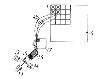
The pixels 1 are supplied with light by the
semiconductor light sources 12 and 13 and 14 (see FIGS. 5
to 8). Said semiconductor light sources preferably are
operated pulsed with a high frequency.
FIG. 5 shows that the light emitted by the
semiconductor light sources 12, 13 and 14 is first
supplied to an optics 155 for homogenizing the flux of
the light, and from there fed into a flexible or semi-
flexible light-conducting fiber bundle 16 with 400
individual fibers, and then supplied by the latter to a
light modulator device 17. In all exemplified
embodiments, said light modulator device 17 is realized
in the form of a solid-state PLZT array with ITO control
and has a total of 400 modulation cells. Each modulation
cell of the light modulator device 17 is connected to a
light-conducting fiber of the light-conducting fiber
bundle 16. The light-conducting fibers 4 lead from each
14
CA 02334403 2000-12-O1
modulation cell of the light modulator device 17 to the
individual pixels 1, whereby the individual light-
conducting fibers 4 can be combined also here to form a
flexible or partially flexible bundle of light-conducting
fibers at least over part of the length.
With such an embodiment of the display module 6 and
of the light supply, the colors red, green and blue are
successively modulated in terms of time.
The exemplified embodiment shown in FIG. 6 differs
from the exemplified embodiment according to FIG. 5 in
that a separate light modulator device 17 is used for
each color. Accordingly, three light-conducting fiber
bundles 16 are required in the present case. Furthermore,
each pixel 1 is connected to three light-conducting
fibers 4 which each are separately connected to the light
modulator device 17 belonging to each color, namely extra
for each color. It is possible in this way to control the
three colors red, green and blue in a parallel manner, so
that a switching frequency reduced by the factor three is
required as compared to the embodiment according to FIG.
5. However, the present embodiment requires three times
as many light-conducting fibers.
The exemplified embodiment according to FIG. 7 is
different from the exemplified embodiment according to
CA 02334403 2000-12-O1
Fig. 6 in that in the present case, each pixel 1 is
subdivided in the sub-pixels la, 1b and lc, of which each
one is responsible for a color red, blue or green, and is
connected to the light modulator device 17 belonging to
said color via the light-conducting fibers 4.
The exemplified embodiment according to FIG. 8
corresponds with the exemplified embodiment according to
the exemplified embodiment according to FIG. 5 with
respect to the light supply; however, the individual
pixels 1 are loosely arranged in the present case and are
formed by the end surfaces of the individual light-
conducting fibers 4. With the present exemplified
embodiment, the format of the display modules 6 can be
varied at any time in any desired way.
FIG. 9 shows that the individual pixels 1 can be
glued also to an optical foil 18, if need be, said foil
being elastically deformable. This results in a flexible
viewing surface of the display module 6, which can be
adapted to any desired spatial form.
It is important in connection with all embodiments
that the light-conducting fibers 4 and the light-
conducting fiber bundles 16 are designed flexible or
partially flexible, so that the pixels 1 or the display
modules 6 assembled from the pixels 1, and the modulator
16
CA 02334403 2000-12-O1
devices 17 or the semiconductor light sources 12, 13, 14
are decoupled from one another in terms of space.
FIG. 10 shows that the pixel 1 may also consist of a
transparent solid body 20 in the form of a truncated
pyramid, if need be, into which the light waveguide
coming from the one side feeds in the form of a light-
conducting fiber 4, and which is provided with a light-
scattering surface 21 on the other side. The transparent
material of such a solid body has a higher refractive
index than air, so that total reflection occurs on the
sides. A great number of such solid bodies 20 can be
combined to form a display module, using suitable
auxiliary means.
In connection with the display module shown in FIG.
11, the individual pixels 1 are located on a through-
extending board 23 consisting of transparent material.
Light waveguides in the form of the light-conducting
fibers 4 feed into said board from one side, namely
separately for each pixel 1. On the opposite side, the
transparent board 23 is provided with a transparent
light-scattering surface 24 that is transparent as well
and serves as the end viewing surface. In the present
case, the board 23 provides for the cohesion of the
display module.
17
CA 02334403 2000-12-O1
In connection with all exemplified embodiments, the
flexible or partially flexible light waveguides 4, 16 can
be wholly or partly embedded in a curing compound after
they have been associated and arranged in the three-
dimensional manner. In this way, the flat display screen
as defined by the invention is rendered more insensitive
to mechanical damage and shocks.
Deviating from the exemplified embodiments shown,
the light waveguides 16 each can be formed within the
zone between the semiconductor light sources 12, 13, 14
and the light modulator devices 17 by a solid body having
a three-dimensional, light-conducting structure that is
forming the light waveguides.
18