Note: Descriptions are shown in the official language in which they were submitted.
CA 02334418 2001-02-07
Title: Power Supply for Lamps
Field of the Invention
[0001] This invention relates to power supplies for certain lamps. More
particularly, the invention may be used to prolong the useful life of lamps
that exhibit a
progressive degradation in light energy output in response to the application
of
electrical power, such as arc: lamps.
Background of the Inventiori
[0002] A photo-initiated adhesive is responsive to light energy when in liquid
form to begin setting into a solid form. The photo-initiated adhesive must be
exposed
to a pre-determined amount of light energy in order for the setting process to
begin.
Light energy of various wavelengths may be used, depending on the particular
photo-
initiated adhesive. In many cases, arc lamps are used to provide the required
light
energy.
[0003] A known problem with arc lamps is that they exhibit a progressive
degradation in their light energy output during their useful service lives. An
arc lamp
typically has a sealed region containing a gas which may be under pressure and
a
pair of electrodes separated by a gap. The gas may comprise mercury, argon,
zenon
and other gases. A voltage potential is applied across the electrodes by a
power
supply, causing an arc to be generatecl in the gap. The arc causes the gas in
the gap
and the region adjacent to the gap to form a plasma, which emits light. The
wavelength of the emitted light depends on the gas used.
[0004] The lamp usual',ly has a reflector which focuses most of the emitted
light
into a light delivery device, such as a fiber optic light guide. The light
delivery device is
used to direct the light onto the photo-initiated adhesive. The reflector may
be said to
provide an optical coupling between the lamp and the light delivery device.
The optical
coupling is configured to direct a known amount of light into the light
delivery device,
when the lamp is in new coridition.
[0005] Over time, the electrodes in the lamp deteriorate in response to the
electrical power applied across them. Typically, the rate of this
deterioration is higher
-1-
CA 02334418 2001-02-07
when a larger power signal is applied to the lamp. As the electrodes
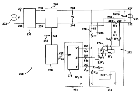
deteriorate, the
gap between them becomes larger. T'he larger gap length increases the
impedance
of the lamp, resulting in the lamp drawing less current from the power supply.
Also,
the larger gap length requires a larger voltage potential across the
electrodes to
maintain the arc. As the current drawn by the lamp falls, the power consumed
by the
lamp also falls. The degradation of the electrodes and the corresponding drop
in
power drawn by the lamp would normally reduce the light emitted by the lamp.
[0006] To prevent the light output of the lamp from falling, the lamp's power
supply is typically configured to apply a constant amount of power by
increasing the
voltage applied to the lamp during the Ilifetime of the lamp, as the current
drawn by the
lamp falls. The constant povrer input results in a relatively constant light
output from
the lamp.
[0007] The larger gap length also results in a longer arc and a
correspondingly
larger physical volume of plasma from which light energy is emitted. As the
volume of
plasma increases and more generally, as the shape of that volume changes, the
optical coupling between the lamp and the light delivery device may become
less
efficient, resulting in less light being directed into the light delivery
device, despite the
fact that the light output from the lamp remains relatively constant. The
reduced
amount of light being coupled into the light delivery device directly reduces
the amount
of light energy that may be used to expose a photo-initiated adhesive.
[0008] The life of the electrodes may be extended by applying a smaller power
signal across them. However, this solution has the disadvantage that the lamp
will
emit less light. Furthermore, the electrodes will still deteriorate, (although
at a slower
rate) and accordingly, the light coupled into and emitted from the light
delivery device
will still decline during the life of the larnp.
[0009] The effect of reduced light being coupled into the light delivery
device
during the service life of the lamp may be partially compensated for by
increasing the
power applied to the lamp during its life, rather than keeping the power level
constant.
As the lamp ages, the increased power input results in an increased light
output from
the lamp. The increased light output may compensate (at least in part) for the
-2-
CA 02334418 2001-02-07
degraded optical coupling between the lamp and the light delivery device by
slowing
the absolute reduction in light energy focused into the light delivery device.
[0010] One power supply that implements this solution provides a power output
adjustment for manually adjusting the power level applied to the lamp. In this
system,
a user initially sets the power level to a fraction of the rated power level
of the lamp.
Then as the lamp ages, the i.iser periodically increases the power level
applied to the
lamp. Eventually, the lamp b~urns out or is replaced for another reason. The
user
must then reset the power level to the initial level for the new lamp. This
manual
system has several disadvantages. First, a user may forget or neglect to
periodically
increase the power applied to the lamp resulting in a low light output level
from the
lamp. Second, if the user has adjusted the power signal to a high level during
the life
of one lamp and then does not return it to its proper initial level when a new
lamp is
installed, the new lamp will deteriorate more rapidly. Third, a user will
normally have
no way of knowing what power level should be set for a previously used lamp
which is
being re-installed, unless the user recorded the setting when the lamp was
removed.
Fourth, the user may intentioinally set the power signal to its highest level
in order to
increase the light output of the lamp. This will defeat the purpose of the
adjustment
and result in the lamp having a short useful service life. In combination,
these
disadvantages are likely to lead to the adjustment being ignored or used
incorrectly.
[0011] Accordingly, there is a need for an improved power supply for use with
lamps that exhibit a change in the size and shape of the arc resulting in a
change in
their light energy output in response to the application of a power signal.
Preferably,
the new power supply will automatically adjust the power supplied to the lamp.
When
used with an arc lamp, the irriproved power supply will preferably reduce the
rate of
deterioration of the electrodes of lamp, thereby reducing the rate at which
the light
energy output of the lamp degrades, as well as reducing the effects of light
coupling
degradation.
Summary of the Invention
[0012] The present invention provides a power supply for a lamp which exhibits
an erosion of its electrodes or of another component of the lamp in response
to the
-3-
CA 02334418 2001-02-07
application of an electrical potential to the lamp, resulting in a change in
the power
drawn by the lamp from the power supply. The power supply provides an output
power signal with a current and a voltage component to the lamp. As the
electrodes
of the lamp deteriorate, the lamp's resistance falls and it draws less current
from the
power supply. This fall in the current component of the output power supply is
measured and is used to generate a skewing signal. The voltage across the lamp
is
controlled by the power supply and it is also measured. A control signal is
generated
based on the measured voltage and current components of the output power
signal
applied to the lamp. A feedback loop is used to regulate this control signal
by
'10 increasing the magnitude of the voltage component of output power signal
to (i)
compensate for the fall in the current component of the output power signal
and (ii) in
response to the skewing sigrial, which amplifies the effect of the fall in the
current
component. The voltage cornponent of the output power signal is thus increased
more than is required to keel) the power magnitude of the output power signal
'15 constant in response to the fall in its current component. The power
magnitude thus
rises in response to the fall iri the current component, which is correlated
to the
deterioration of the lamps electrodes and the related change in the size and
shape of
the lamp's light output.
[0013] The power supply of the present invention is configured to initially
power
20 the lamp at a portion of its rai:ed power level. Typically, this portion
will be between
50% and 90% of the rated power level. The portion may be less than 50%,
although
this may cause an undesirable loss in light output from the iamp. More
preferably, the
portion is between 70% and 135% of the rated power of the lamp. During the
life of the
lamp, the power signal is steadily increased in response to the reduction in
current
25 drawn by the lamp. Towards the end of the service life of the lamp, the
power signal
applied to the lamp may be close to the rated power of the lamp.
Brief Description of the Drauvings
[0014] A preferred embodiment of the present invention will now be described
in detail with reference to the drawings, in which:
-4-
CA 02334418 2001-02-07
[0015] Figure 1 illustrates a typical prior art illlumination system for
exposing
photo-initiated adhesives with light energy;
[0016] Figure 2 is a block/schematic diagram of a prior art power supply of
the
system of Figure 1;
[0017] Figure 3 is a graph illustrating the operation of the prior art power
supply
of Figure 2 and of the power supply of Figure 4, below;
[0018] Figure 4 is a block diagram of a power supply according to the present
invention; and
[0019] Figure 5 is a graph illustrating voltage, current and power components
of
an exemplary output power signal of the power supply of Figure 4.
Detailed Description of the Preferred Embodiment
[0020] Reference is first made to Figure 1, which illustrates a prior art
illumination system 100 useci to expose photo-initiated adhesives to light
energy.
System 100 has a power source 102, pair of power input terminals 104, 106, a
power
supply 108, a pair of power output terminals 110, 112, a lamp 114, a reflector
115, a
diaphragm 116, a shutter 118, a light delivery device 120, and a handle 124.
[0021] A power source 102 is coupled to power input terminals 104, 106.
Power source 102 provides an alternating current power signal V;,, across
terminals
104 and 106. Power signal V;n may be a typical municipal AC power supply and
power source 102 may be operated by a typical municipal electric company.
[0022] Power supply 108 receives power signal V;n and provides a DC output
power signal Vout at terminals 110,112, to which lamp 114 is coupled. Lamp 114
emits light in response to power signal Vout.
[0023] Light delivery device 120 imay be a light guide such as an optic fiber,
a
bundle of optic fibers or another other light transmitting element. Typically,
light
delivery device 120 will have a protective cover 121, which may be made of
plastic,
rubber, metal or another material. Typically, light delivery device 120 will
be 4-5 mm in
diameter, although this dimension may vary substantially depending on the
particular
application of illumination system 100.
-5-
CA 02334418 2001-02-07
[0024] Reflector 115 is positioned adjacent to lamp 114 to reflect the emitted
light into light delivery device 120 through diaphragm 116. Diaphragm 116 has
an
opening sized to permit a round spot of light to fall on light delivery device
120. The
light incident on light delivery device 120 is transmitted to the illuminating
end 122 of
the light delivery device 120, which is within and extends through handle 124.
Light
incident on light delivery device 120 from reflector 115 is emitted from the
illuminating
end 122.
[0025] Handle 124 has an illumination control button 125, which is coupled to
shutter 118 by a control circuit (not shown). The control circuit operates to
open
shutter 118 when button 12EI is depressed (as shown in solid outline in Figure
1) and
to close shufter 118 when button 125 in its normal extended position (as shown
in
dotted outline in Figure 1). UVhen shutter 118 is closed, light from lamp 114
is
blocked from entering light delivery device 120 and the illuminating end 122
of light
delivery device 120 does not emit any light. When shutter 118 is open, the
illuminating 122 of light delivery device 120 emits light from lamp 114.
Button 125
allows the operator of systern 100 to open and close shutter 118 to control
the
amount of light emitted from -the illuminating end 122 of light delivery
device 120.
Button 125 may be located iri another position on illumination system 100. For
example, it may be located on the housing of a part of the illumination system
which
contain lamp 114 and power supply 108. Button 125 is shown as part of handle
124
as an example only.
[0026] An operator uses system 100 by placing a photo-initiated adhesive (not
shown) in a liquid form on a selected location (not shown), using handle 124
to point
illumination end 122 of light delivery device 120 at the photo-initiated
adhesive,
depressing button 125 to begin exposing the photo-initiated adhesive to light
from
lamp 114, waiting for a pre-determined amount of time, which has been selected
to
start to photo-initiated adhesive to set into a solid form and releasing
button 125 to
stop exposing the photo-initiated adhesive, which then completes the curing
process.
[0027] Referring still to Figure 1, lamp 114 has a sealed region 147 which
contains a gas such as xenon, argon, rnercury, neon or another gas which emits
light
energy in response to an electrical potential. A pair of electrodes 126, 127,
which are
-6-
CA 02334418 2001-02-07
coupled to power output terminals 110, 112, extend into the sealed region and
have a
gap 128 between them. When power signal Vo,,t is applied to electrodes 126,
127, the
gas in sealed region 147 forms a plasma and begins to emit light. The majority
of
this emitted light is directed onto reflector 115 between lines 129 and 130.
Lamp 114
may have a mirrored surface 131 to ensure that a majority of the the light
emitted by
lamp 114 remains within lines 129 and 130. This light is then directed by
reflector
115 as a light spot 133 onto diaphragm 116. Preferably, spot 133 is only
slightly
larger than the opening 134 in diaphragm 116 and most of the reflect light
passes
through opening 134 onto light delivery device 120.
[0028] Over time, electrodes 126, 127 will erode in response to the power
signal VoUt applied to them. As they erode, the gap 128 between them will
grow. As a
result, the limits of the same relative quantity of light energy which was
initially emitted
by lamp 114 between lines 129, 130 may now be emitted between dotted lines
132,
133. Reflector 115 will now reflect the emitted light onto a larger spot 134
on
diaphragm 116, as indicated by lines 135, 136. As a result, a smaller
proportion of
the light emitted by lamp 114, and a smaller absolute amount of light energy,
is
directed into light delivery device 120. This degradation in the optical
coupling
between lamp 114 and light delivery device 120 results in less light being
available at
the illumination end 122 of light delivery device 120 to expose a photo-
intiated
adhesive, increasing the length of exposure required to start the photo-
initiated
adhesive to set.
[0029] The increased gap 128 between electrodes 126, 127 also changes the
load characteristics of lamp '114. The impedance between the electrodes
increases,
causing the current drawn by lamp 114 from power supply 108 to fall. Power
supply
108 is configured to maintain a constarit level of power to lamp 114 by
increasing the
voltage component of power signal Vout. This is described in greater detail
below.
The constant power input into lamp 114 results in lamp 114 emitting a
relatively
constant amount of light, however, the degraded optical coupling still results
in less
light being directed into light delivery device 120.
[0030] Reference is next made to Figure 2, which illustrates prior art power
supply 108 in block diagram -format. Power supply 108 includes an off-line
power
-7-
CA 02334418 2001-02-07
stage 137, a DC-DC power stage 140, an output power monitoring stage 148, an
output power calculating sta(je 164 and an output voltage control stage 168.
[0031] Off-line power stage 137 is coupled to terminals 104 and 106 to receive
input power signal V;n. DC-E)C power stage 140 may be configured to filter
switching
transients, EMI and other forms of noise from input power signal V;n. Off-line
power
stage 137 provides a "clean" DC power signal V, corresponding to input power
signal
V;n at terminals 138 and 139.
[0032] DC-DC power stage 140 is coupled to terminals 138 and 139 to receive
power signal V, and is also coupled to an output power control terminal 141
from
which it receives an output power control signal 142. DC-DC power stage 140
produces a power signal V2 corresponding to output power control signal 142 at
terminals 143 and 144. Typically, power signal V2 will be a DC signal, which
is
suitable for powering lamp 114.
[0033] The construction of off-line power stage 137 and DC-DC power stage
140 will be understood by those skilled in the art and they are not described
here in
detail. Either of off-line power stage 137 or DC-DC power stage 140 may be
configured to rectify the power signal (V;,, or Vj) received by that element
so that power
signal VZ will be a DC rectified signal with a magnitude smaller than that of
power
signal V. Output power control signal 142 may operate DC-DC power stage 140 as
a constant current, constant voltage or constant power supply. The constant
current
and constant voltage modes are required during the turn-on and warm-up phases
of
an arc lamp. For the purposes of the present example, output power control
signal
142 regulates DC-DC power stage 140 as a constant power supply.
[0034] Terminal 143 is coupled directly to a first power output terminal 110.
Power output terminal 144 is coupled to a second power output terminal 112
through
a current sensing element 150, which is part of output power monitoring stage
148.
Typically, current sensing element 150 will be a resistor with a relatively
small
resistance (i.e. 0.01.0), and therefore will have a relatively small voltage
drop across it.
Current sensing element may also be another device such as a Hall effect
current
sensor. As a result of the small voltage drop across sensing element 150, an
output
power signal Vout with a magnitude close to that of power signal V2 will exist
across
-8-
CA 02334418 2001-02-07
output terminals 110 and 11;2. Lamp 114 is coupled to terminals 110 and 112 to
receive output power signal \/out.
[0035] Terminal 144 is coupled to a reference point 145, which has a reference
voltage level. Typically, reference point 145 will have the same voltage as
point 139.
Signals produced by output voltage monitoring stage 148 are referenced to this
reference voltage. Reference point 145 may be an internal ground point for
power
supply 108 and may have a reference voltage of 0 volts, although this is not
necessary.
[0036] Output power nionitoring stage 148 is coupled to terminals 143, 144 and
'10 112 to monitor the voltage and current components of power signal Vout.
[0037] Terminal 143 is coupled to a voltage monitoring terminal 152 of output
power monitoring stage 148. Terminals 144 and 112 are coupled respectively to
a
first current monitoring termirial 158 and a second current monitoring
terminal 160 of
output power monitoring stage 148.
[0038] Output power monitoring stage 148 has a voltage monitoring circuit 170
which comprises a pair of resistors R, and R2. Resistors R, and R2 are coupled
in
series between terminal 152 and reference point 145 forming a voltage divider
and
provide signal Vps at a terminal 162. Signal Vps is referenced to the
reference voltage
of reference point 145 and has a magnitude that is a fraction of the magnitude
of the
voltage component of power signal V2, which in turn has a magnitude almost
identical
to the magnitude of output power signal Vout.
[0039] Output power rrionitoring stage 148 also has a current monitoring
circuit
172 which comprises current sensing element 150, resistors R4, R5, R6 and R7,
a
capacitor C, and a differentiail amplifier 174. Current sensing element 150 is
a
resistor R3 coupled between current monitoring terminals 158 and 160. Resistor
R4
is coupled between terminal 158 and the negative input terminal of
differential
amplifier 174. Resistor R5 is coupled between terminal 160 and the positive
input
terminal of differential amplifier 174. Resistors R4 and R5 act as input
resistors for
differential amplifier 174 and present a voltage signal Vd;ff across the
positive and
negative inputs of differential amplifier '174. Vd;ff corresponds to the
voltage difference
between terminals 144 and 112, which in turn is proportional to the current
I,amp in
-9-
CA 02334418 2001-02-07
lamp 114. Capacitor C, is coupled in parallel with resistor R3 and operates to
decouple high frequency noise which may be present across terminals 158 and
160
from the inputs of amplifier 174. Resistors R6 and R7 are coupled between the
output
of differential amplifier 174 and its negative input terminal to provide a
negative
feedback loop. Resistor R7 is a variable resistor with relatively small
resistance and
may be adjusted to control the resistarice in the feedback loop, thereby
allowing the
amplification of differential amplifier 174 to be controlled.
[0040] Differential amplifier 174 is a linear amplifier and produces signal
Ips at
terminal 156. Signal Ips is proportional to the current I,amp flowing in lamp
114.
[0041] Output power monitoring stage 148 thus provides signal Vps and Ips
which correspond to the voltage and current components of the output power
signal
Vout supplied to lamp 114. In the preferred embodiment of the present
invention, the
components of output power monitoring stage 148 are selected so that signals
VPS
and IpS are between 0 to 10 volts
[0042] Output power calculating stage 164 comprises an analog multiplier 176
and a zener diode Dl. Multiplier 176 has a pair of inputs X and Y and an
output W
which is calculated as follows:
w- XxY
[0043] Output power calculating stage 164 is coupled to terminals 156 and 162
to receive signals Vps and Ips. Output power calculating stage 164 produces a
signal
Pps at a terminal 166. Signal PpS is equal to:
Pn, _ VPS x I ps
[0044] Terminal 156 is coupled to the X input of multiplier 176 and terminal
162
is coupled to the Y input of multiplier 176. The W output of multiplier 176 is
coupled to
25 terminal 166 and forms signal Pps. Since signal Vps at terminal 162 is
proportional to
the voltage across lamp 114 and since signal Ips at terminal 156 is
proportional to the
current flowing through lamp 114, the signal Pps is proportional to the power
supplied
to lamp 114.
-10-
CA 02334418 2001-02-07
Zener diode D, is coupled between terminal 162 and ground in order to protect
the Y
input of multiplier 176. Resistors R, and R2 are generally selected so that
the
magnitude of signal VpS does not exceed the maximum safe level of the Y input.
However, this could occur if i:he magnitude power output signal Vout exceeds a
particular level. Zener diode D, limits the maximum voltage at the Y input of
multiplier
176 to a safe level.
[0045] Output power control stage 168 receives output power signal Pps and
provides a pulse width modulated (PWM) output power control signal 142 in
response. Output power coritrol stage 168 is a PWM signal generation circuit,
which
may be of known construction. Output power control stage 168 is configured to
vary
output power control signal 142 in order to keep signal PpS constant (i.e.
such that
lamp 114 draws a constant amount of power from power supply 20).
[0046] DC-DC power stage 140 is responsive to PWM output power control
signal 142 to vary the voltage component of power signal V2, thereby varying
the
voltage component of output power signal VoUt.
[0047] Prior art power supply 108 is configured to produce a constant power
output at output terminals 110 and 112, so that lamp 114 receives a constant
amount
of power from output power signal VoUt. Output power monitoring stage 148,
output
power calculating stage 164 and output power control stage 168 form a closed
feedback loop which monitors and controls the output voltage Vout produced by
DC-DC
power stage 140. Output power control stage 168 varies output power control
signal
142 so that output power signal Pps remains constant.
[0048] Output power control stage 168 has a conventional design, and a
person skilled in the art will be capable of producing it. Accordingly, the
structure of
output power control stage 168 has not been shown or described in detail.
[0049] As lamp 114 ages, the current and voltage components of output power
signal Vout will change. For example, if an exemplary lamp 114 is a 100 W
mercury
vapour arc lamp, its initial power requirements may be 5 A at 20 V. As lamp
114 ages,
its electrodes will deteriorate and the resistance it presents across
terminals 110 and
112 will rise. Since output power signal Voõt is voltage regulated, the
voltage may be
considered constant on an instantaneous basis. As the resistance of lamp 114
rises,
-11-
CA 02334418 2001-02-07
the current flowing through it will fall and the power drawn by lamp 114 will
fall,
causing signal Pps to fall, on an instantaneous basis. Output power control
block
stage 168 will respond by increasing the magnitude of power signal V2, which
will in
turn cause DC-DC power stage 140 to increase the magnitude of output power
signal
Vout. This will increase the magnitude of signal VpS and signal Pps. After
some time,
the voltage and current components of output power signal Vout may be 4 A and
25V.
The magnitude of voltage component output power signal VoUt will be
progressively
increased in this fashion, unt:il signal Pps is restored to its initial value,
or until the
voltage component of power output signal Vout oan no longer be increased. This
will
'10 occur if a maximum voltage or power output limit of DC-DC power stage 140
is
reached. The power drawn by lamp 114 is kept constant in this way, up to a
maximum voltage level.
[0050] Reference is next made to Figure 3. As the electrodes of lamp 114
deteriorate, the size of the spot 133 (Figure 1) of light reflected on
diaphragm 116 will
increase, as described abovE:, despite the fact that lamp 114 draws a
relatively
constant amount of power from power supply 108 and emits a relatively constant
amount of light. Data line 180 indicates the average light output level 180 at
the
illumination end 122 (Figure 1) of the light delivery device 120 of
illumination system
100 using prior art power supply 108, as shown in Figure 1. The lamps used to
obtain the data for line 180 were of a group of 100W mercury arc lamps
supplied with
100W of power by power supply 20. Figure 3 was produced from experimental data
using several such lamps. The particular lamps used for the experiment were
rated
for a typical service life of 1000 hours. The initial light output level of
the illumination
end 122 of the light delivery device 120 is rated as 100%. Over time, the
light output
level falls and after approximately 620 hours the light output had fallen to
about 50% of
its initial level. After less thari 900 hours, the light output level had
fallen well below
20% of its initial level.
[0051] Reference is next made to Figure 4, which illustrates a power supply
208
according to the present invention. Components of power supply 208 which
correspond to components of prior art power supply 108 are identified by
similar
reference numerals increaseci by 100 or by adding a prime symbol (') to them.
The
-12-
CA 02334418 2001-02-07
structure and operation of off-line power stage 237, DC-DC power stage 240 and
output power control stage 268 are identical to the operation of the
corresponding
components in prior art power supply '108.
[0052] Output power monitoring stage 248 has a voltage monitoring circuit 270
which is identical to voltage monitoring circuit 170 and which is coupled to
terminal
262, where it provides signal V'ps, which corresponds to the magnitude of the
voltage
component of output power signal V'oõt. Output power monitoring circuit 248
also has
a current monitoring circuit 272, which is coupled terminals 244 and 212.
Current
monitoring circuit 248 produces a signal Ips which corresponds to the
magnitude of
the current component of output power signal Vo,,t,(i.e. the current I',amp
flowing through
lamp 214) at terminal 256.
[0053] Current monitoring circuit 272 also comprises resistors R8, R9 and Rlo
and a voltage source 278. Resistor RIo is an adjustable resistor. Resistors
R8, R9
and Rlo are coupled in series between terminal 256 and voltage source 278. In
a
preferred embodiment of povver supply 208, voltage source 278 supplies a
constant
negative bias voltage V278 of --5V. Resistors R8, R9 and RIo form a voltage
divider and
shifter. This voltage divider and shifter provides a skewing signal Sps at the
node
between R8 and R9, which is coupled to terminal 284. Skewing signal SpS has a
magnitude equal to:
Snr= (t4j+R10) Ips-V278
(R8+R9+R,o
[0054] Typically, R8, Rc,, Rlo and V278 will be selected so that skewing
signal Sps
has a magnitude that is smaller than Ipõ but which has a larger proportional
rate of
change. Signals Ips and Sps have the same sign at all times.
[0055] Output power calculating stage 264 comprises a multiplier/summer 276
and a zener diode D'I. Multiplier/summer 276 has X' and Y' inputs similar to
the X and
Y inputs of multiplier 176. Multiplier/summer 276 also has an additional input
Z, and
the output W' is calculated as follows:
W'== Xf XYt + Z.
-13-
CA 02334418 2001-02-07
[0056] The Z input of output power calculating stage 264 is coupled to
terminal
284 to receive skewing signal S'PS. Multiplier/summer 276 produces a signal
P'ps at
terminal 266 as follows:
, ,
P~ _ Vp' X Ip'. + S.
pS 10 ns
[0057] Signal P'pS is not proportional to the power drawn by lamp 214 from
power supply 220, but is "skewed" by skewing signal Sps. As the current I'iamp
through
lamp 214 falls, the magnitude of signall I'pS will fall. This in turn will
cause the
magnitude of signal Sps to fall, however, the rate of change in skewing signal
SpS will
be larger than the rate of change in signal Ips (based on the resistances of
resistors
R8, R9 and Rlo and the magriitude of negative bias voltage supply 278). As
lamp 214
ages and draws less current I',amp from power supply 220, the effect of signal
SpS will
be to increase the rate at whlich signal P'pS falls compared to the rate at
which signal
Pps of power supply 108 falls, (A person skilled in the art will understand
that signal
P'ps does not actually fall in rnagnitude over time, due to the feedback
control affected
by output power control block 268. However, on an instantaneous basis, the
magnitude of signal P'ps may be considered to have fallen in response to the
decrease in current I'iamp drauvn by lamp 214.)
[0058] Output power control stage 268 is coupled to terminal 266 to receive
signal P'ps and provides a PVVM output control signal 242 at a terminal 241.
Output
power control block 268 operates in the same way as output power control stage
168
to maintain signal P'ps at a constant level. Since signal P'pS will fall
faster than signal
PPs of power supply 108 (on an instantaneous basis), it will appear to output
power
control block 268 that the power drawn by lamp 214 has decreased by a larger
amount than it has actually decreased by. In response, output power control
stage
268 will vary PWM output control signal 242 to increase the magnitude of the
voltage
component of PWM output control signal 242 so that the power delivered to lamp
214
actually increases rather thari remaining constant, as it did in prior art
power supply
108.
-14-
CA 02334418 2001-02-07
[0059] In a preferred embodiment of power supply 208, the components of
output power monitoring sta(le 248 and output power calculating stage 264 have
the
following values:
Component Value
R'1 13.3 kS')
R'2 2 kS2
R'3 0.0152
R'4 240 S2
R'5 300 S)
R'6 20 k.Q
R'7 Potentiometer 10 kS)
R'$ 12 ks2
R'9 18 ks2
R', o Potentiometer 5kf2
C', 100 nF
D', 12 V, 500 mW Zener
[0060] Power supply 208 is preferably used as follows. Output power control
block 268 is configured to regulate P'ps such that magnitude of output power
signal
V'oUt.(in Watts) is lower than the rated power level of lamp 214, when lamp
214 is new.
Typically, the initial power level of output power signal V'out will be
between
approximately 50% and approximately 90% of the rated power for lamp 214. For
example, if lamp 214 is a 100 W lamp, then output power control block 268 may
be
configured to initially set output control signal 242 so that the power
magnitude of
output power signal V'out is between about 50 to about 90 W.
[0061] Reference is next made to Figure 5. In the preferred embodiment of
power supply 208, output povver control block 268 has been configured such
that
output voltage signal V'out has an initial magnitude of 80 W. Lamp 214 is
selected to
have a rated power of 100 W. Figure 5 illustrates the voltage and current
components
and power magnitude (Lamp Power) of output power signal V'out during one
-15-
CA 02334418 2001-02-07
experiment conducted using the preferred embodiment of power supply 208. The
voltage component is shown as data line 286. The current component is shown as
data line 288. The power magnitude is shown as line 290. As the electrodes of
lamp
214 deteriorate over its useful life, the current drawn by lamp 214 falls as
shown in
line 288. In response, signal P'pS (not shown in Figure 5) falls (on an
instantaneous
basis) in a skewed manner clue to the addition of skewing signal in the
calculation of
signal P'ps. Output power control stage 268 regulates the signal P'ps to keep
it
constant by varying output power control signal 242 to increase the voltage
component (line 286) of output power signal V'oUt. Due to the skewing of
signal P'pS,
the increase in the voltage component of output power signal V'out is
sufficient to
increase the power magnitude (line 290) of output power signal VoUt. The power
supplied to (or drawn by) lamp 214 is thus increased as the current drawn by
lamp
214 decreases.
[0062] By applying an initial power output signal V'out with a power magnitude
'15 less than the rated power of lamp 214, power supply 208 reduces the rate
at which
the electrodes of lamp 214 deteriorate. Thus, the effects of electrode
deterioration are
slowed.
[0063] Referring still to Figure 5, the voltage component of the output power
signal V;oõt appears to fall be'tween about 85 hours and 200 hours of
operation of
lamp 214. Since the voltage componerit of output power signal V'out is
regulated by
output power control stage 2E38 to maintain signal P'ps constant, an increase
in signal
P'pS will result in the voltage component. This may occur when the resistance
of lamp
214 between terminals 210 and 212 rises and thereby causes lamp 214 to draw
more current from power supply 208. During such periods, the power applied to
lamp
214 will fall. In general, however, the power magnitude of output power signal
V'out will
steadily increase. Power supply 208 is responsive in this way to the actual
performance of a particular laimp 214 as the lamp 214 ages.
[0064] Reference is again made to Figure 3. Line 280 indicates the average
light output from the light delivery device 120 of an illumination system 100,
when
power supply 208 is used in the place of power supply 108. A series of 100 W
mercury test lamps similar to those used to calculate line 180 were used to
obtain the
-16-
CA 02334418 2001-02-07
data for line 280. Since the power applied to lamp 214 during its service life
is
increased, then on a momentary basis, the actual amount of light produced by
the
lamp is increased. Although electrode degradation still results in the size of
spot 133
increasing in size, the resulting decrease in the amount of light emitted from
the
illumination end 122 of the light delivery device 120 is reduced, since a
greater
quantity of light energy will be coupled in the light delivery device 120,
than if the light
energy output of the lamp was constant. As a result, the light output at the
illumination
end 122 of light delivery device 120 (line 280) falls more slowly than the
lamp 114
powered by prior art power supply 108 (line 280).
[0065] Applying a lower initial power to lamp 214 with power supply 208
resulted in an initial reductiori in the light output of at the illumination
end 122
compared to when power supply 108 was used. In the present example, power
supply 208 was configured to provide 80 W of power to lamp 214 initially. The
initial
light output with power supply 208 fell to approximately 75% that of the
initial light
'15 output when power supply 108 was used. However, the slower reduction in
the light
output at the illumination end with power supply 208 (line 280) than in the
case of
prior art power supply 108:
1. After about 130 hours of operation, the light output at the illumination
ends 122 was within 15% of the light output of lamp 114.
2. After about 600 hours of operation, the light output at the illumination
end
122 using power supply 208 exceeded that using power supply 108.
3. Lamp 114 generally failed or had a light output below 20% of its initial
power after aboiut 900 hours of operation with power supply 108, despite
the fact that the lamp was rated for 1000 hours of service. In contrast,
lamp 214 had a light output of more than 35% of the initial light output of
lamp 114, even after 1400 hours of operation with power supply 208.
[0066] The specific performance characteristics illustrated in Figures 2 and 4
and stated above are only exemplary.
[0067] As noted earlier, the initial power of output voltage signal V'oUt is
preferably between 50% and 90% of the rated power of lamp 214. Although an
initial
power level less than 50% of the rated power of lamp 214 (i.e. 50 W) may be
used,
-17-
CA 02334418 2001-02-07
this may result in an undesirably low light output level from lamp 214 and at
the
illumination end 122 of light cieiivery device 120. The inventors have found
that a
reasonable balance between: (i) a reduced initial light output from lamp 214
due to
the reduction in the input povuer level; (ii) the benefit of increased light
output later in
the life of lamp 214; and (iii) the increase in the service life of lamp 214
is found when
the initial power level appiiecd to lamp 214 is between 70% and 85% of the
lamp's
rated power. The inventor has found that when power supply 208 initially
provides
80% of a mercury arc lamp's rate power to the lamp, the lamp produces about
75% of
the light energy it produced with power input of 100% of its rated power.
[0068] A preferred embodiment of the present invention has been described.
Furthermore, the invention has been described for use with an arc lamp which
exhibit
electrode deterioration in response to a power signal. The present power
supply is
suitable for use with any lamp or related device which exhibits a degradation
in its
performance in response to the magnitude of the voltage component of the power
signal applied to it.
[0069] Other variations of the present invention will be apparent to a person
skilled in the art. All such variations fall within the spirit and scope of
the present
invention, which is limited only by the following claims.
-18-
_.r_